Note : Les descriptions sont présentées dans la langue officielle dans laquelle elles ont été soumises.
CA 02931657 2016-05-25
DESCRIPTION
Title of Invention
POWER CONVERSION DEVICE
Technical Field
[0001] The present disclosure relates to a power conversion device using
a current
resonant inverter.
Background Art
[0002] Power conversion devices for converting a DC voltage into an AC
voltage
with medium- and high-frequency resonant inverters using current resonance are
used for
applications such as railcars or solar power generation (see Patent Literature
1). A
current resonant inverter creates a moment at which a current is zero using
resonance of
an LC circuit within a switching circuit, and turns off a power semiconductor
switch
element at the timing, thereby reducing switching loss. The current resonance
causes
turn-off loss of the power semiconductor to be substantially zero, which
advantageously
provides a power conversion device with low losses.
[0003] When a switch is activated at a frequency different from a
resonance
frequency of the inverter circuit, the resonant inverter may have a risk of
breaking a
switch element because an off-resonance occurs and an overcurrent passes
through the
switch. For example, Patent Literature 2 discloses a control method for
preventing a
switch element from breaking due to an off-resonance in a series resonant
converter.
Patent Literature 2 discloses a half-bridge current resonant converter in
which a current of
a secondary rectifier diode, which does not flow during a steady operation (at
a normal
frequency), is detected to determine an off-resonance.
[0004] Patent Literature 3 discloses a method for controlling an induction-
heating
power source, in which when a switching loss at turn-off exceeds an allowable
setpoint in
a full-bridge current resonant inverter, operation of the inverter is stopped.
Patent
CA 02931657 2016-05-25
2
Literature 4 discloses a control circuit for a switching power source, in
which, when an
off-resonance is detected from a detected value of an output current of a
complex current
resonant converter, a switch element is turned off. Patent Literature 4 also
discloses that
a signal for turning a switch element on is blocked while a current flowing
through an
impedance element is detected with both of two switch elements turned off.
Citation List
Patent Literature
[0005] Patent Literature 1: US Patent Application Publication No.
2008/0055941
Patent Literature 2: Unexamined Japanese Patent Application Kokai Publication
No. 2010-187478
Patent Literature 3: Unexamined Japanese Patent Application Kokai Publication
No. 2010-153089
Patent Literature 4: Unexamined Japanese Patent Application Kokai Publication
No. 2011-135723
Summary of Invention
Technical Problem
[0006] When a resonance frequency of an inverter circuit changes for
some reason,
a power semiconductor switch element is turned off in a state in which current
flows
through the switch element, thus increasing turn-off loss. During such
operation, as the
current resonant inverter is a medium- and high-frequency circuit, the loss of
the power
semiconductor increases rapidly. Then, a temperature detector mounted on a
base
surface of a cooler for cooling the power semiconductor may fail to detect a
rapid change
in temperature of the power semiconductor. This failure may cause a junction
temperature of the power semiconductor to exceed its limit before the over-
temperature
protection of the inverter circuit operates, which leads to breakdown. For
example, a
current shutdown state occurs whenever the resonance frequency of the circuit
decreases
due to cutting of a portion of a transformer winding, a short circuit thereof,
or the like.
CA 02931657 2016-05-25
3
The power semiconductor switch element requires protection from the current
shutdown
state.
[0007] The temperature-based protection approach involves stopping the
switching
operation when the temperature detected by a thermistor exceeds a given
temperature.
However, this approach does not allow the power semiconductor to be protected
from the
over-temperature condition. Thus, the current shutdown state of the power
semiconductor is detected to stop the switching operation. For example, when
the
switch element is turned off immediately after detection of the off-resonance,
detection of
the off-resonance due to effects of noises or the like also causes the
inverter to stop
temporarily. However, for applications, such as electric railcars, in which
frequent
shutdowns of the power supply are undesirable, continuous running as long as
possible is
required.
[0008] The present disclosure is made to solve the above described
problems, and
an objective of the present disclosure is to protect a switch element of a
resonant inverter
circuit and to prevent excessive stoppage of the resonant inverter circuit
when a
resonance frequency of the resonant inverter circuit changes.
Solution to Problem
[0009] A power conversion device according to the present disclosure
includes a
resonant inverter circuit including two or more switch elements, a detector to
detect an
output current of the switch elements, a resonance determiner, and a
controller. The
resonance determiner determines that a resonance frequency of the resonant
inverter
circuit is abnormal when a number of times an absolute value of a current
detected by the
detector at turn-off of the switch elements is equal to or greater than a
threshold is equal
to or greater than a predetermined number of times that is two or more during
a
predetermined period that is at least twice a switching period of the switch
elements.
The controller causes the switching operation of the resonant inverter circuit
to stop when
the resonance determiner determines that the resonance frequency of the
resonant inverter
CA 02931657 2016-05-25
4
circuit is abnormal.
Advantageous Effects of Invention
[0010] According to the techniques of the present disclosure, when the
number of
times the absolute value of the current detected by the detector at turn-off
of the switch
elements is equal to or greater than a threshold is equal to or greater than a
predetermined
number of times that is two or more during a predetermined period that is
equal to or
longer than two switching periods, the resonance frequency of the resonant
inverter
circuit is determined as being abnormal and the switching operation is
stopped, which
protects the switch elements of the resonant inverter circuit and prevents
excessive
stoppage of the resonant inverter circuit when the resonance frequency of the
resonant
inverter circuit changes.
Brief Description of Drawings
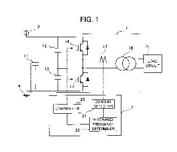
[0011] FIG. 1 is a block diagram illustrating an example arrangement of
a power
conversion device according to an embodiment of the present disclosure;
FIG. 2 is a diagram illustrating current waveforms of a normal resonance
frequency of a resonant inverter circuit;
FIG. 3 is a diagram illustrating current waveforms at decreased resonance
frequency of the resonant inverter circuit;
FIG. 4 is a diagram illustrating an example of a logic circuit of a resonance
frequency determiner;
FIG. 5 is a flowchart illustrating an example operation of stop processing
during a
resonance frequency abnormality, according to Embodiment 1 of the present
disclosure;
FIG. 6 is a flowchart illustrating an example operation of stop processing
during a
resonance frequency abnormality, according to Embodiment 2 of the present
disclosure.
Description of Embodiments
[0012] Embodiment 1
FIG. 1 is a block diagram illustrating an example arrangement of a power
CA 02931657 2016-05-25
conversion device according to an embodiment of the present disclosure. The
power
conversion device includes a resonant inverter circuit 1 and a control device
2. The
resonant inverter circuit 1 is connected to a DC power source 3 and a ground
4, and
receives DC power supplied by the DC power source 3. The control device 2
activates
5 the resonant inverter circuit 1 to cause the resonant inverter circuit 1
to convert the DC
voltage into an AC voltage and supply the AC power to a load circuit 5.
[0013] The resonant inverter circuit 1 includes a filter capacitor 11,
resonant
capacitors 12 and 13, switch elements 14 and 15, a resonant transformer 16,
and a
detector 17. The filter capacitor 11 blocks noises of the DC power source 3 to
reduce a
variation in voltage applied to the switch elements 14 and 15.
[0014] The resonant capacitors 12 and 13 are connected in series. Before
the start
of operation of the resonant inverter circuit 1, the divided DC voltages are
each applied to
the corresponding one of the resonant capacitors 12 and 13. The values of the
capacitances of the resonant capacitors 12 and 13 may be the same or
different. When
the resonant capacitors 12 and 13 have the same capacitance, the voltages of
the
capacitors are the same. The resonant capacitors 12 and 13 may be constituted
by a
plurality of capacitors connected in series and/or in parallel. In that case,
the
capacitances of the resonant capacitors 12 and 13 are combined capacities of
the
pluralities of capacitors. The switch elements 14 and 15 may also be
constituted by a
plurality of elements.
[0015] Although FIG. 1 illustrates as an example the switch elements 14
and 15
each as an insulated gate bipolar transistor (IGBT), the switch elements 14
and 15 are not
limited to the 1GBT, but can be any element controllable with a gate signal.
The switch
elements 14 and 15 are connected in series and are connected to the resonant
capacitors
12 and 13 in parallel.
[0016] The resonant transformer 16 includes a primary winding and a
secondary
winding, and both ends of the primary winding of the resonant transformer 16
are each
CA 02931657 2016-05-25
6
connected to a corresponding connection point, that is, a connection point
between the
resonant capacitors 12 and 13 or a connection point between the switch
elements 14 and
15. The detector 17 is disposed between one end of the resonant
transformer 16 and the
connection point between the switch elements 14 and 15, and outputs a voltage
proportional to the output current of the switch elements 14 and 15.
[0017] The control device 2 alternately turns the switch elements 14 and
15 on and
off to cause the resonant capacitors 12 and 13 and the resonant transformer 16
to
cooperate together to generate an AC voltage across the resonant transformer
16. The
control device 2 starts activating the resonant inverter circuit 1, for
example, when an
input voltage directed to the resonant inverter circuit 1 and detected by an
unillustrated
input voltage detector falls into a predetermined range. The control device 2
stops the
resonant inverter circuit 1, for example, when the input voltage to the
resonant inverter
circuit 1 exceeds a threshold and exhibits an overvoltage.
[0018] It is assumed that the resonant capacitors 12 and 13 have the
same value of
capacitance and the control device 2 outputs a gate signal that enables the
switch element
14 to be turned on for a predetermined conduction time at the start of
operation of the
resonant inverter circuit 1. The control device 2 outputs a gate signal so
that the switch
elements 14 and 15 are alternately turned on for the conduction time during
operation of
the resonant inverter circuit 1. A short-circuit protection time is also
provided in which
the switch elements 14 and 15 are both turned off.
[0019] While the switch element 14 is turned on and the switch element
15 is
turned off, a current passes from the DC power source 3, through the switch
element 14,
the resonant transformer 16, and the resonant capacitor 13, to the ground 4.
While the
switch element 15 is turned on and the switch element 14 is turned off, a
current passes
from the DC power source 3, through the resonant capacitor 12, the resonant
transformer
16, and the switch element 15, to the ground 4.
[0020] Because the resonant transformer 16 and the resonant capacitor 12
are
CA 02931657 2016-05-25
7
connected in series or the resonant transformer 16 and the resonant capacitor
13 are
connected in series, a current oscillates at a resonance frequency determined
by an
inductance of the resonant transformer 16 and the capacitances of the resonant
capacitors
12 and 13. The switching loss can be reduced by turning off the switch
elements 14 and
15 when the current is zero.
[0021] FIG. 2 illustrates current waveforms of normal resonance
frequency of the
resonant inverter circuit. The upper graph of FIG. 2 shows a current of the
switch
element 14. The lower graph of FIG.2 shows a current detected by the detector
17. As
the switch element 15 is turned on while the switch element 14 is turned off,
the detected
current appears alternately as positive or negative.
[0022] As illustrated in FIG. 2, the current changes so as to oscillate
at the
resonance frequency determined by the resonant transformer 16 and the resonant
capacitors 12 and 13. Then, the current of the switch element is turned off
while the
current is zero. Here, when the resonance frequency determined by the resonant
transformer 16 and the resonant capacitors 12 and 13 decreases for some
reason, a period
of the current oscillation increases. In that case, when the switch elements
14 and 15 are
turned off at the same timing after the switch elements 14 and 15 have been
turned on,
the current still flows at the turn-off timing.
[0023] FIG. 3 illustrates current waveforms at decreased resonance
frequency of the
resonant inverter circuit. As can been seen, the resonance current has a
longer period,
and the current thus still flows at turn-off of the switch elements 14 and 15.
[0024] The control device 2 of FIG. 1 includes a current detector 21, a
resonance
frequency determiner 22, and a controller 23. The current detector 21 performs
analog-to-digital conversion of a voltage proportional to the voltage detected
by the
detector 17 to output a current value. The resonance frequency determiner 22
determines that the resonance frequency of the resonant inverter circuit 1 is
abnormal
when a number of times an absolute value of the current detected by the
detector 17 at
CA 02931657 2016-05-25
8
turn-off of the switch elements 14 and 15 is equal to or greater than a
threshold is a
predetermined number of times that is two or more during a predetermined
period that is
at least twice a switching period of the switch elements 14 and 15. The
controller 23
stops the switching operation of the resonant inverter circuit 1 when the
resonance
frequency determiner 22 determines that the resonance frequency of the
resonant inverter
circuit 1 is abnormal. The control device 2 also stops the resonant inverter
circuit 1
when the current detected by the detector 17 and flowing into the resonant
transformer 16
exceeds a threshold and becomes an overcurrent.
[0025] The conditions for the resonance frequency determiner 22 to
determine that
the resonance frequency is abnormal can be determined as appropriate for
properties and
use of the resonant inverter circuit 1. The conditions can be freely set
within a range in
which M> N> 2, where the determination period is M times the switching period
(M is
an integer equal to or greater than 2), and Nis a defined number of times that
the absolute
value of the current detected by the detector 17 at turn-off of the switch
elements 14 and
15 is equal to or greater than a threshold for the resonance frequency to be
determined to
be abnormal (Nis an integer equal to or greater than 2).
[0026] FIG. 4 is a diagram illustrating an example of a logic circuit of
a resonance
frequency determiner. The resonance frequency determiner 22 uses a comparator
26 to
compare a current value output by the current detector 21 versus a threshold
of a register
24 for each turn-off of the switch elements 14 and 15, for example. The
comparator 26
then outputs, to a shift register 28 and an adder 29, "1" for the current
value equal to or
greater than the threshold and "0" for the current value less than the
threshold. M-1 shift
registers (flip-flops) 28 are connected in series, where the switching cycle
time interval
for determination is M periods (M is an integer equal to or greater than 2).
The output of
the last shift register 28 is input to a subtractor 30. The subtractor 30
receives an input
of a result of the adder 29 and subtracts the output of the last shift
register 28 from the
result of the adder 29.
CA 02931657 2016-05-25
9
[0027] The result of the subtractor 30 is input to a comparator 27 and
returned to
the adder 29 in the next period. The adder 29 and the subtractor 30 cooperate
together
for addition of the current result of the comparator 26 and subtraction of the
result M
periods earlier of the comparator 26. The comparator 27 compares the result of
the
subtractor 30 with a defined number of times of the register 25 (for example,
N), and
outputs, to the controller 23, "1 (abnormal resonance frequency)" when the
comparison
result is equal to or greater than the defined number of times and "0 (normal
resonance
frequency)" when the comparison result is less than the defined number of
times. As a
result, the resonance frequency determiner 22 determines that the resonance
frequency is
abnormal when the number of times the absolute value of the current detected
by the
detector 17 at turn-off of the switch elements 14 and 15 is equal to or
greater than a
threshold is equal to or greater than the defined number of times (N) during a
period that
is Mtimes the switching period.
[0028] The current at turn-off of the switch elements 14 and 15 may be
detected
only when either one of the switch elements 14 and 15 is turned off, or may be
detected
only when both the switch elements 14 and 15 are turned off. The determination
period
of current detection when both the switch elements 14 and 15 are turned off is
a half that
of current detection when either one thereof is turned off.
[0029] FIG. 5 is a flowchart illustrating an example operation of stop
processing
during a resonance frequency abnormality, according to Embodiment I. The
resonance
frequency determiner 22 initially sets a counter to zero (step S01). The
counter
indicates the number of times the absolute value of the current detected by
the detector 17
at turn-off of the switch elements 14 and 15 is equal to or greater than a
threshold. Then,
the current value detected by the detector 17 is input for each turn-off of
the switch
elements 14 and 15 (step SO2).
[0030] The current value is compared to a threshold, and if the current
value is
equal to or greater than the threshold (step S03; YES), 1 is added to the
counter (step
CA 02931657 2016-05-25
SO4). If the current value is less than the threshold (step S03; NO), the
counter value
remains the same. Then, if the current value Mperiods earlier (M is an integer
equal to
or greater than 2) is equal to or greater than a threshold (step S05; YES), 1
is subtracted
from the counter (step S06). If the current value Mperiods earlier (/1/ is an
integer equal
5 to or greater than 2) is less than a threshold (step S05; NO), the
counter value remains the
same.
[0031] The counter value is compared to the defined number of times, and
if the
counter value is equal to or greater than the defined number of times (step
S07; YES), the
switching operation of the resonant inverter circuit 1 is stopped (step S08).
If the
10 counter value is less than the defined number of times (step S07; NO),
the processing
returns to step S02 and restarts with input of the current value.
[0032] As described above, the power conversion device of Embodiment 1
determines that the resonance frequency of the resonant inverter circuit 1 is
abnormal
when the number of times the absolute value of the current detected by the
detector 17 at
turn-off of the switch elements 14 and 15 is equal to or greater than the
threshold is equal
to or greater than the predetermined number of times that is two or more
during a
predetermined period that is at least twice a switching period, and then the
switching
operation is stopped. As a result, when the resonance frequency of the
resonant inverter
circuit 1 changes, the switch elements 14 and 15 of the resonant inverter
circuit 1 are
protected, and excessive stoppage of the resonant inverter circuit 1 is
prevented.
[0033] Embodiment 2
In Embodiment 2, a resonance frequency abnormality is determined when a
number of times an absolute value of a current detected by a detector 17 for
each turn-off
of switch elements 14 and 15 is equal to or greater than a threshold continues
to be equal
to or greater than a defined number of times. Specifically, this condition
corresponds to
M= N> 2 in the configuration of Embodiment 1, which means that the A/ periods
that are
a determination period (M is an integer equal to or greater than 2) are equal
to a defined
CA 02931657 2016-05-25
11
number of times N used for determining that the resonance frequency is
abnormal (N is
an integer equal to or greater than 2).
[0034] FIG. 6 is a flowchart illustrating an example operation of stop
processing
during a resonance frequency abnormality, according to Embodiment 2. A
resonance
frequency determiner 22 initially sets a counter to zero (step S11). The
counter
indicates the number of times the absolute value of the current detected by
the detector 17
at turn-off of the switch elements 14 and 15 is equal to or greater than a
threshold. Then,
the current value detected by the detector 17 is input for each turn-off of
the switch
elements 14 and 15 (step S12).
[0035] The current value is compared to a threshold, and if the current
value is
equal to or greater than the threshold (step S13; YES), 1 is added to the
counter (step
S14). If the current value is less than the threshold (step S13; NO),
processing returns to
step Sll and restarts with a reset of the counter (set to 0).
[0036] After 1 is added to the counter in step SI4, the counter value is
compared to
a defined number of times, and if the counter value is equal to or greater
than the defined
number of times (step S15; YES), the switching operation of the resonant
inverter circuit
I is stopped (step S16). If the counter value is less than the defined number
of times
(step S15; NO), the process is returned to step S12 without resetting of the
counter and
repeated from an input of the current value.
[0037] As stated above, according to Embodiment 2, the abnormal resonance
frequency is determined to occur when the number of times the absolute value
of the
current detected by the detector 17 for each turn-off of the switch elements
14 and 15 is
equal to or greater than the threshold continues to be equal to or greater
than the defined
number of times. This thus allows for simple configuration of the resonance
frequency
determiner 22.
[0038] In the above embodiments, to facilitate understanding, the
described
example power conversion devices generate single-phase AC and have a single
leg that
CA 02931657 2016-05-25
12
includes an upper arm (switch element 14) and a lower arm (switch element 15).
However, the configuration of embodiments can also be applied to a power
conversion
device that generates three-phase AC and has three legs. For the three-phase
AC type of
the power conversion device, detectors 17 are each provided in the
corresponding one of
the legs to detect the output current of each leg to ensure detection and
determination of a
resonance frequency abnormality.
[0039] The power conversion devices of the embodiments can also be
configured to
use, as the switch elements 14 and 15, switch elements made of a wide band gap
semiconductor having a wider band gap than that of silicon. The wide band gap
semiconductor is, for example, silicon carbide, gallium nitride-based
material, or
diamond. The switch element made of wide band gap semiconductor has a high
voltage
withstand capability and a high allowable current density. Such
characteristics allow for
a reduced size of the switch element, and use of the reduced size of the
switch element
thus allows for a reduced size of a semiconductor module incorporating the
switch
element.
[0040] The wide band gap semiconductor has high heat resistance, thus
allowing
reduction in size of heat radiation fins of a heat sink and the use of air for
cooling of a
water cooler, which enable the size of the semiconductor module to be further
reduced.
Furthermore, the lower power loss allows higher efficiency in the switch
element, and
thus allows a more highly efficient semiconductor module.
[0041] Preferably, both of the switch elements 14 and 15 are made of the
wide band
gap semiconductor, but either one of the switch elements may be made of the
wide band
gap semiconductor. In that case, the effect described in Embodiment 1 can also
be
obtained.
Reference Signs List
[0042] 1 Resonant inverter circuit
2 Control device
CA 02931657 2016-05-25
13
3 DC power source
4 Ground
Load circuit
11 Filter capacitor
5 12, 13 Resonant capacitor
14, 15 Switch element
16 Resonant transformer
17 Detector
21 Current detector
22 Resonance frequency determiner
23 Controller
24, 25 Register
26, 27 Comparator
28 Shift register
29 Adder
30 Subtractor