Note : Les descriptions sont présentées dans la langue officielle dans laquelle elles ont été soumises.
CA 02945901 2016-10-20
282204
ADDITIVE MANUFACTURING SYSTEMS
INCLUDING AN IMAGING DEVICE AND METHODS
OF OPERATING SUCH SYSTEMS
BACKGROUND
[0001] The subject matter disclosed herein relates generally to additive
manufacturing
systems and, more particularly, to additive manufacturing systems including
imaging
devices for imaging melted particulate during an additive manufacturing
process.
[0002] At least some additive manufacturing systems involve the buildup of a
metal
component to make a net, or near net shape component. These systems produce
complex
components from expensive materials at a reduced cost and with improved
manufacturing
efficiency. Some known additive manufacturing systems, such as Direct Metal
Laser
Melting (DMLM), Selective Laser Sintering (SLS), Direct Metal Laser Sintering
(DMLS),
Selective Laser Melting (SLM) and LaserCusing systems, fabricate components
using a
focused energy source, such as a laser device or an electron beam generator,
and a
particulate, such as a powdered metal.
[0003] In some known additive manufacturing systems, component quality is
reduced
due to excess heat and/or variation in heat being transferred to the metal
powder by the
focused energy source within the melt pool. For example, sometimes local
overheating
occurs, particularly at overhangs. In addition, in some known additive
manufacturing
systems, component surface quality, particularly at overhangs or downward
facing
surfaces, is reduced due to the variation in conductive heat transfer between
the powdered
metal and the surrounding solid material of the component. For example, the
melt pool
produced by the focused energy source sometimes becomes too large resulting in
the
melted metal spreading into the surrounding powdered metal as well as the melt
pool
penetrating deeper into the powder bed, pulling in additional powder into the
melt pool.
The increased melt pool size and depth, and the flow of molten metal result in
a poor
surface finish of the overhang or downward facing surface.
1
CA 02945901 2016-10-20
282204
[0004] In addition, in some known additive manufacturing systems, the
component's
dimensional accuracy and small feature resolution is reduced due to melt pool
variations
because of the variability of thermal conductivity of the subsurface
structures and metallic
powder. As the melt pool size varies, the accuracy of printed structures
varies, especially
at the edges of features.
[0005] At least some known additive manufacturing systems include imaging
devices to
generate images of portions of the melt pool during the fabrication process.
The imaging
devices include a camera with a shutter that is opened for extremely short
periods of time.
The imaging devices track the focused energy source to capture light during
the melting
process. However, the imaging devices generate images of only portions of the
melt pool.
Moreover, the imaging devices generate images of portions of the melt pool
without
reference to specific positions. In addition, the imaging devices require
complex
programming and apparatus customized for the specific additive manufacturing
system.
BRIEF DESCRIPTION
[0006] In one aspect, an additive manufacturing system includes a surface
holding a
particulate and a focused energy source configured to generate at least one
beam that moves
along the surface to heat the particulate to a melting point creating a melt
path. A camera
is configured to generate an image of the surface as the at least one beam
moves along the
surface. The camera has a field of view and is positioned in relation to the
surface such
that the field of view encompasses a portion of the melt path defining a
plurality of rasters.
The camera generates a time exposure image of at least the portion of the melt
path defining
the plurality of rasters.
[0007] In another aspect, a method of manufacturing a part using an additive
manufacturing system includes depositing a layer of particulate on a surface.
The
particulate is heated to a melting point of the particulate using a focused
energy source. A
beam of the focused energy source is directed at the particulate and a melt
pool is formed
that emits a melt pool light. The beam is moved to generate a melt pool path.
A camera is
2
CA 02945901 2016-10-20
282204
exposed to the melt pool light and a time exposure image is generated of at
least a portion
of the melt pool path with the camera.
[0008] In yet another aspect, an imaging device for use in an additive
manufacturing
system including a surface holding a particulate and a focused energy source
configured to
generate at least one beam that moves along the surface to heat the
particulate to a melting
point is provided. The imaging device includes a camera. The camera includes a
sensor
and a casing defining an aperture for light to travel through and strike the
sensor. The
imaging device further includes a trigger configured to receive a signal
relating to an
operating characteristic of the focused energy source and to control the
travel of light
through the aperture based on the signal such that the camera generates a time
exposure
image of the particulate during operation of the focused energy source.
DRAWINGS
[0009] These and other features, aspects, and advantages of the present
disclosure will
become better understood when the following detailed description is read with
reference to
the accompanying drawings in which like characters represent like parts
throughout the
drawings, wherein:
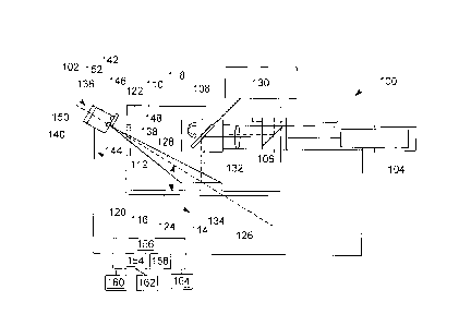
[0010] FIG. 1 is a schematic view of an exemplary additive manufacturing
system
including an exemplary imaging device;
[0011] FIGS. 2 is a photograph of an exemplary time exposure image generated
using
the imaging device shown in FIG. 1 during operation of the additive
manufacturing system
shown in FIG. 1;
[0012] FIG. 3 is a photograph of an exemplary time exposure image generated
using the
imaging device shown in FIG. 1 during formation of a component including an
overhanging feature; and
3
CA 02945901 2016-10-20
282204
[0013] FIG. 4 is a photograph of an exemplary time exposure image generated
using the
imaging device shown in FIG. 1 during formation of a component including an
overhanging feature.
[0014] Unless otherwise indicated, the drawings provided herein are meant to
illustrate
features of embodiments of the disclosure. These features are believed to be
applicable in
a wide variety of systems comprising one or more embodiments of the
disclosure. As such,
the drawings are not meant to include all conventional features known by those
of ordinary
skill in the art to be required for the practice of the embodiments disclosed
herein.
DETAILED DESCRIPTION
[0015] In the following specification and the claims, reference will be made
to a number
of terms, which shall be defined to have the following meanings.
[0016] The singular forms "a", "an", and "the" include plural references
unless the
context clearly dictates otherwise.
[0017] "Optional" or "optionally" means that the subsequently described event
or
circumstance may or may not occur, and that the description includes instances
where the
event occurs and instances where it does not.
[0018] Approximating language, as used herein throughout the specification and
claims,
may be applied to modify any quantitative representation that could
permissibly vary
without resulting in a change in the basic function to which it is related.
Accordingly, a
value modified by a term or terms, such as "about", "approximately", and
"substantially",
are not to be limited to the precise value specified. In at least some
instances, the
approximating language may correspond to the precision of an instrument for
measuring
the value. Here and throughout the specification and claims, range limitations
may be
combined and/or interchanged, such ranges are identified and include all the
sub-ranges
contained therein unless context or language indicates otherwise.
4
CA 02945901 2016-10-20
282204
[0019] As used herein, the terms "processor" and "computer," and related
terms, e.g.,
"processing device," "computing device," and "controller" are not limited to
just those
integrated circuits referred to in the art as a computer, but broadly refers
to a
microcontroller, a microcomputer, a programmable logic controller (PLC), and
application
specific integrated circuit, and other programmable circuits, and these terms
are used
interchangeably herein. In the embodiments described herein, memory may
include, but it
not limited to, a computer-readable medium, such as a random access memory
(RAM), a
computer-readable non-volatile medium, such as a flash memory. Alternatively,
a floppy
disk, a compact disc ¨ read only memory (CD-ROM), a magneto-optical disk
(MOD),
and/or a digital versatile disc (DVD) may also be used. Also, in the
embodiments described
herein, additional input channels may be, but are not limited to, computer
peripherals
associated with an operator interface such as a mouse and a keyboard.
Alternatively, other
computer peripherals may also be used that may include, for example, but not
be limited
to, a scanner. Furthermore, in the exemplary embodiment, additional output
channels may
include, but not be limited to, an operator interface monitor.
[0020] Further, as used herein, the terms "software" and "firmware" are
interchangeable,
and include any computer program storage in memory for execution by personal
computers, workstations, clients, and servers.
[0021] As used herein, the term "non-transitory computer-readable media" is
intended to
be representative of any tangible computer-based device implemented in any
method of
technology for short-term and long-term storage of information, such as,
computer-
readable instructions, data structures, program modules and sub-modules, or
other data in
any device. Therefore, the methods described herein may be encoded as
executable
instructions embodied in a tangible, non-transitory, computer-readable medium,
including,
without limitation, a storage device and/or a memory device. Such
instructions, when
executed by a processor, cause the processor to perform at least a portion of
the methods
described herein. Moreover, as used herein, the term "non-transitory computer-
readable
media" includes all tangible, computer-readable media, including, without
limitation, non-
transitory computer storage devices, including without limitation, volatile
and non-volatile
CA 02945901 2016-10-20
282204
media, and removable and non-removable media such as firmware, physical and
virtual
storage, CD-ROMS, DVDs, and any other digital source such as a network or the
Internet,
as well as yet to be developed digital means, with the sole exception being
transitory,
propagating signal.
[0022] Furthermore, as used herein, the term "real-time" refers to at least
one of the time
of occurrence of the associated events, the time of measurement and collection
of
predetermined data, the time to process the data, and the time of a system
response to the
events and the environment. In the embodiments described herein, these
activities and
events occur substantially instantaneously.
[0023] As used herein, the terms "time exposure image" and "long exposure
image" refer
to an image generated by exposing a sensor of an imaging device to light for
an extended
period of time.
[0024] The systems and methods described herein relate to additive
manufacturing
systems, such as Direct Metal Laser Melting (DMLM) systems. The embodiments
described herein include a focused energy source and an imaging device. During
operation
of the focused energy source, the imaging device generates a time exposure
image of a
melted particulate forming a melt pool. In some embodiments, substantially the
entire melt
pool is captured in the time exposure image. The time exposure image
illustrates intensity
of light emitted throughout the melt pool. In some embodiments, the time
exposure image
is inspected to determine variations and defects in the additive manufacturing
process. As
a result, errors in the additive manufacturing process are corrected and the
process is
improved. In some embodiments, the time exposure image is used in a feed-
forward
process to improve the manufacturing of subsequent components.
[0025] FIG. 1 is a schematic view of an exemplary additive manufacturing
system 100
including an imaging device 102. In the exemplary embodiment, the additive
manufacturing system is a direct metal laser melting (DMLM) system. Additive
manufacturing system 100 further includes a focused energy source 104
optically coupled
to optics 106 and galvanometers 108 for controlling the scanning of focused
energy source
6
CA 02945901 2016-10-20
282204
104. In the exemplary embodiment, focused energy source 104 is a laser device.
In
alternative embodiments, additive manufacturing system 100 includes any
focused energy
sources 104 that enable additive manufacturing system 100 to operate as
described herein.
For example, in some embodiments, additive manufacturing system 100 has a
first focused
energy source 104 having a first power and a second focused energy source 104
having a
second power different from the first power. In further embodiments, additive
manufacturing system 100 has at least two focused energy sources 104 having
substantially
the same power output. In further embodiments, additive manufacturing system
100
includes at least one focused energy source 104 that is an electron beam
generator.
[0026] In the exemplary embodiment, additive manufacturing system 100 further
includes a housing 110 defining a surface 112 configured to hold a particulate
114.
Housing 110 includes a bottom wall 116 defining surface 112, a top wall 118
opposite
bottom wall 116, and a sidewall 120 at least partially extending between
bottom wall 116
and top wall 118. In alternative embodiments, housing 110 includes any walls
and surfaces
that enable additive manufacturing system 100 to operate as described herein.
In the
exemplary embodiment, sidewall 120 defines a viewport 122 therein. In
alternative
embodiments, viewport 122 is defined by any portion of housing 110 that
enables additive
manufacturing system 100 to operate as described herein. For example, in some
embodiments, viewport 122 is at least partially defined by top wall 118. In
further
embodiments, housing 110 defines a plurality of viewports 122.
[0027] In the exemplary embodiment, imaging device 102 is positioned adjacent
viewport 122 on the exterior of housing 110. An image axis 126 extends between
imaging
device 102 and particulate 114 on surface 112. Accordingly, in the exemplary
embodiment, image axis 126 extends through viewport 122. Imaging device 102 is
spaced
a distance 124 from surface 112 measured along image axis 126. In particular,
image axis
126 extends through aperture 148 of imaging device 102. In some embodiments,
distance
124 is in a range between about 15 centimeters (cm) (6 inches (in.)) and about
152 cm (60
in.). In further embodiments, distance 124 is in a range between about 30 cm
(12 in.) and
about 91 mm (36 in.). In the exemplary embodiment, distance 124 is
approximately 61 cm
7
CA 02945901 2016-10-20
282204
(24 in.) In alternative embodiments, imaging device 102 is spaced any distance
124 from
surface 112 that enables imaging device 102 to operate as described herein. In
the
exemplary embodiment, image axis 126 makes an angle 128 with surface 112. In
some
embodiments, image axis 126 and surface 112 make an angle 128 in a range
between about
70 and about 40 . In further embodiments, image axis 126 and surface 112 make
an angle
128 in a range between about 80 and about 20 . In the exemplary embodiment,
image
axis 126 and surface 112 make an angle 128 of approximately 45 . In
alternative
embodiments, angle 128 is any angle that enables imaging device 102 to operate
as
described herein.
[0028] As used herein, the term "field of view" refers to the extent of an
object that
imaging device 102 captures in an image. In the exemplary embodiment, the
field of view
of imaging device 102 is in reference to surface 112 and depends on the
position and
orientation of imaging device 102 in relation to surface 112. The field of
view of imaging
device 102 is adjusted by adjusting components of imaging device 102, such as
optics, and
the distance between surface 112 and imaging device 102. In the exemplary
embodiment,
imaging device 102 has a field of view of surface 112 of approximately 250
millimeters
(mm) x 250 mm. In alternative embodiments, imaging device 102 has any field of
view
that enables imaging device 102 to operate as described herein. For example,
in some
embodiments, imaging device 102 is disposed adjacent top wall 118 and has a
field of view
of surface 112 of approximately 250 mm x 280 mm. In further embodiments, a
plurality
of imaging devices 102 are used to a create a field of view sufficient to
cover a larger
surface 112 without substantially reducing resolution.
[0029] In the exemplary embodiment, additive manufacturing system 100 also
includes
a computer control system, or controller 130. Galvanometers 108 are controlled
by
controller 130 and deflect a beam 132 of focused energy source 104 along a
predetermined
path on surface 112. In some embodiments, galvanometers 108 include two-
dimension
(2D) scan galvanometers, three-dimension (3D) scan galvanometers, dynamic
focusing
galvanometers, and/or any other galvanometer system that deflect beam 132 of
focused
8
CA 02945901 2016-10-20
282204
energy source 104. In alternative embodiments, galvanometers 108 deflect a
plurality of
beams 132 along at least one predetermined path.
[0030] Additive manufacturing system 100 is operated to fabricate a component
134 by
a layer-by-layer manufacturing process. Component 134 is fabricated from an
electronic
representation of the 3D geometry of component 134. In some embodiments, the
electronic
representation is produced in a computer aided design (CAD) or similar file.
In alternative
embodiments, the electronic representation is any electronic representation
that enables
additive manufacturing system 100 to operate as described herein. In the
exemplary
embodiment, the CAD file of component 134 is converted into a layer-by-layer
format that
includes a plurality of build parameters for each layer. In the exemplary
embodiment,
component 134 is arranged electronically in a desired orientation relative to
the origin of
the coordinate system used in additive manufacturing system 100. The geometry
of
component 134 is sliced into a stack of layers of a desired thickness, such
that the geometry
of each layer is an outline of the cross-section through component 134 at that
particular
layer location. A "toolpath" or "toolpaths" are generated across the geometry
of a
respective layer. The build parameters are applied along the toolpath or
toolpaths to
fabricate that layer of component 134 from the material used to construct
component 134.
The steps are repeated for each respective layer of component 134 geometry.
Once the
process is completed, an electronic computer build file (or files) is
generated including all
of the layers. The build file is loaded into controller 130 of additive
manufacturing system
100 to control the system during fabrication of each layer.
[0031] After the build file is loaded into controller 130, additive
manufacturing system
100 is operated to generate component 134 by implementing the layer-by-layer
manufacturing process, such as a DMLM method. The exemplary layer-by-layer
additive
manufacturing process does not use a pre-existing article as the precursor to
the final
component, rather the process produces component 134 from a raw material in a
configurable form, such as particulate 114. For example, without limitation, a
steel
component is additively manufactured using a steel powder. Additive
manufacturing
system 100 enables fabrication of components using a broad range of materials,
for
9
CA 02945901 2016-10-20
282204
example, without limitation, metals, ceramics, and polymers. In alternative
embodiments,
DMLM fabricates components from any materials that enable additive
manufacturing
system 100 to operate as described herein.
[0032] As used herein, the term "parameter" refers to characteristics that are
used to
define the operating conditions of additive manufacturing system 100, such as
a power
output of focused energy source 104, a vector scanning speed of focused energy
source
104, a raster power output of focused energy source 104, a raster scanning
speed of focused
energy source 104, a raster tool path of focused energy source 104, and a
contour power
output of focused energy source 104 within additive manufacturing system 100.
In some
embodiments, the parameters are initially input by a user into controller 130.
The
parameters represent a given operating state of additive manufacturing system
100. In
general, during raster scanning, beam 132 is scanned sequentially along a
series of
substantially straight lines spaced apart and parallel to each other. During
vector scanning,
beam 132 is generally scanned sequentially along a series of substantially
straight lines or
vectors, where the orientations of the vectors relative to each other
sometimes varies. In
general, the ending point of one vector coincides with the beginning point of
the next
vector. Vector scanning is generally used to define the outer contours of a
component,
whereas raster scanning is generally used to "fill" the spaces enclosed by the
contour,
where the component is solid.
[0033] In the exemplary embodiment, imaging device 102 includes a camera 136
including a lens 138, a sensor 140, a casing 142, a filter 144, and a shutter
146. Casing 142
defines an aperture 148 for light to enter an interior space 150 defined by
casing 142. Lens
138, filter 144, and shutter 146 are disposed adjacent aperture 148. Lens 138
directs and
focuses light on sensor 140, which is disposed in interior space 150. Filter
144 filters light
and inhibits overexposure of sensor 140. In the exemplary embodiment, filter
144 is
configured to reduce the intense light emitted by focused energy source 104.
In alternative
embodiments, camera 136 is includes any components that enable imaging device
102 to
operate as described herein.
CA 02945901 2016-10-20
282204
[0034] In the exemplary embodiment, shutter 146 is positionable between an
open
position that allows light to travel through aperture 148 and a closed
position that inhibits
light traveling through aperture 148. In the exemplary embodiment, shutter 146
is
configured to be maintained in the open position and in the closed position
for
predetermined periods of time. For example, in some embodiments, shutter 146
is in the
open position for a period of time longer than about 1 minute. In further
embodiments,
shutter 146 is in the open position for a period of time longer than about ten
minutes. In
the exemplary embodiment, shutter 146 is in the open position for a period of
time in a
range between about 1 minute and about 10 minutes. In some embodiments, the
period of
time is determined at least in part based on the build time of a component
formed by
additive manufacturing system 100. In alternative embodiments, shutter 146 is
in the open
position and in the closed position for any periods of time that enable
imaging device 102
to operate as described herein. For example, in some embodiments, shutter 146
moves
between the open position and the closed position in a sequence of exposures
that are
configured to generate the time exposure image. In some embodiments, the total
time
shutter 146 is in the open position during the sequence of exposures is longer
than about 1
minute. The sequence of exposures reduces the amount of stray light from
adjacent
portions of the build that is included in the time exposure image. As a
result, in some
embodiments, the time exposure image generated from a sequence of exposures is
more
detailed with than an image generated from an exposure with the shutter
maintained in the
open position.
[0035] In the exemplary embodiment, imaging device 102 includes a triggering
component 152 to control exposure of sensor 140 to light. Triggering component
152
facilitates shutter 146 being in the open position such that sensor 140 is
exposed to
sufficient light to generate a time exposure image. In alternative
embodiments, triggering
component 152 is any mechanism that enables imaging device 102 to operate as
described
herein. In the exemplary embodiment, triggering component 152 receives a
signal relating
to an operating characteristic of focused energy source 104. For example, in
some
embodiments, triggering component 152 receives a signal at the commencement
and
11
CA 02945901 2016-10-20
282204
completion of a layer build. In some embodiments, triggering component
receives a signal
based on the amount of light in the melt pool during operation of focused
energy source
104. In further embodiments, triggering component 152 receives signals based
on input
data, sensor information, and any other information that enables imaging
device 102 to
operate as described herein. In some embodiments, based on the received
signals,
triggering component 152 causes shutter 146 to move to the open position or
the closed
position and remain in the selected position for a predetermined time period
or until
triggering component 152 receives another signal.
[0036] During operation of imaging device 102, shutter 146 is positioned in
the open
position such that light is allowed to travel through aperture 148 and strike
sensor 140. The
light activates sensor 140 and is converted to electronic signals. In the
exemplary
embodiment, sensor 140 includes a plurality of pixels (not shown) that are
activated by
light. In alternative embodiments, sensor 140 is any sensor that enables
imaging device
102 to operate as described herein. In the exemplary embodiment, shutter 146
is moved
from the open position to the closed position and an image is generated based
on the
exposure of sensor 140 while shutter 146 was in the open position. In
alternative
embodiments, shutter 146 is moved between the open position and the closed
position
while the shutter is exposed to light. The time exposure image is generated
based on the
cumulative exposure of sensor 140 and/or based on digitally summing distinct
exposures.
In the exemplary embodiment, the image is transmitted to a processor 154
coupled to
camera 136. In some embodiments, processor 154 is configured to recognize
differences
in light intensity in the image.
[0037] In the exemplary embodiment, shutter 146 is moved to the open position
prior to
focused energy source 104 generating beam 132. Shutter 146 is maintained in
the open
position such that sensor 140 is activated by light emitted from the weld pool
as beam 132
moves along the weld pool. When shutter 146 is moved to the closed position, a
time
exposure image of the weld pool is generated. In alternative embodiments,
shutter 146 is
moved to the open position and the closed position at any times that enable
additive
manufacturing system 100 to operate as described herein. For example, in some
12
CA 02945901 2016-10-20
282204
embodiments, shutter 146 is moved to the open position after activation of
focused energy
source 104 and moved to the closed position prior to deactivation of focused
energy source
104.
[0038] In the exemplary embodiment, controller 130 is any controller typically
provided
by a manufacturer of additive manufacturing system 100 to control operation of
additive
manufacturing system 100. In some embodiments, controller 130 is a computer
system
that includes at least one processor (not shown) and at least one memory
device (not
shown). In some embodiments, controller 130 includes, for example, a 3D model
of
component 134 to be fabricated by additive manufacturing system 100. In some
embodiments, controller 130 executes operations to control the operation of
additive
manufacturing system 100 based at least partially on instructions from human
operators.
Operations executed by controller 130 include controlling power output of
focused energy
source 104 and adjusting galvanometers 108 to control the scanning speed of
focused
energy source 104 within additive manufacturing system 100.
[0039] In the exemplary embodiment, a computing device 156 is coupled to
imaging
device 102 and focused energy source 104. Computing device 156 includes a
memory
device 158 and processor 154 coupled to memory device 158. In some
embodiments,
processor 154 includes one or more processing units, such as, without
limitation, a multi-
core configuration. In the exemplary embodiment, processor 154 includes a
field
programmable gate array (FPGA). Alternatively, processor 154 is any type of
processor
that permits computing device 156 to operate as described herein. In some
embodiments,
executable instructions are stored in memory device 158. Computing device 156
is
configurable to perform one or more operations described herein by programming
processor 154. For example, processor 154 is programmed by encoding an
operation as
one or more executable instructions and providing the executable instructions
in memory
device 158. In the exemplary embodiment, memory device 158 is one or more
devices that
enable storage and retrieval of information such as executable instructions or
other data.
In some embodiments, memory device 158 includes one or more computer readable
media,
such as, without limitation, random access memory (RAM), dynamic RAM, static
RAM,
13
CA 02945901 2016-10-20
282204
a solid-state disk, a hard disk, read-only memory (ROM), erasable programmable
ROM,
electrically erasable programmable ROM, or non-volatile RAM memory. The above
memory types are exemplary only, and are thus not limiting as to the types of
memory
usable for storage of a computer program.
[0040] In some embodiments, memory device 158 is configured to store build
parameters
including, without limitation, real-time and historical build parameter
values, or any other
type of data. In the exemplary embodiment, memory device 158 stores images
generated
by imaging device 102. In alternative embodiments, memory device 158 stores
any data
that enable additive manufacturing system 100 to operate as described herein.
In some
embodiments, processor 154 removes or "purges" data from memory device 158
based on
the age of the data. For example, processor 154 overwrites previously recorded
and stored
data associated with a subsequent time or event. In addition, or
alternatively, processor
154 removes data that exceeds a predetermined time interval. In addition,
memory device
158 includes, without limitation, sufficient data, algorithms, and commands to
facilitate
monitoring and measuring of build parameters and the geometric conditions of
component
134 fabricated by additive manufacturing system 100.
[0041] In some embodiments, computing device 156 includes a presentation
interface
160 coupled to processor 154. Presentation interface 160 presents information,
such as
images generated by imaging device 102, to a user. In one embodiment,
presentation
interface 160 includes a display adapter (not shown) coupled to a display
device (not
shown), such as a cathode ray tube (CRT), a liquid crystal display (LCD), an
organic LED
(OLED) display, or an "electronic ink" display. In some embodiments,
presentation
interface 160 includes one or more display devices. In addition, or
alternatively,
presentation interface 160 includes an audio output device (not shown), for
example,
without limitation, an audio adapter or a speaker (not shown).
[0042] In some embodiments, computing device 156 includes a user input
interface 162.
In the exemplary embodiment, user input interface 162 is coupled to processor
154 and
receives input from the user. In some embodiments, user input interface 162
includes, for
14
CA 02945901 2016-10-20
282204
example, without limitation, a keyboard, a pointing device, a mouse, a stylus,
a touch
sensitive panel, such as, without limitation, a touch pad or a touch screen,
and/or an audio
input interface, such as, without limitation, a microphone. In further
embodiments, a single
component, such as a touch screen, functions as both a display device of
presentation
interface 160 and user input interface 162.
[0043] In the exemplary embodiment, a communication interface 164 is coupled
to
processor 154 and is configured to be coupled in communication with one or
more other
devices, such as imaging device 102, and to perform input and output
operations with
respect to such devices while performing as an input channel. For example, in
some
embodiments, communication interface 164 includes, without limitation, a wired
network
adapter, a wireless network adapter, a mobile telecommunications adapter, a
serial
communication adapter, or a parallel communication adapter. Communication
interface
164 receives a data signal from or transmits a data signal to one or more
remote devices.
For example, in an alternative embodiment, communication interface 164 of
computing
device 156 communicates with controller 130.
[0044] Presentation interface 160 and communication interface 164 are both
capable of
providing information suitable for use with the methods described herein, such
as,
providing information to the user or processor 154. Accordingly, presentation
interface
160 and communication interface 164 are referred to as output devices.
Similarly, user
input interface 162 and communication interface 164 are capable of receiving
information
suitable for use with the methods described herein and are referred to as
input devices.
[0045] FIG. 2 is a photograph of a time exposure image 200 generated using
imaging
device 102 during operation of additive manufacturing system 100. Time
exposure image
200 shows a melt pool including a plurality of rasters 202. As used herein,
the term
"rasters" refers to a series of parallel lines along a melt path. As shown in
FIG. 2, rasters
202 are alternately light, i.e., more intense, and dark, i.e., less intense.
The direction of
travel of beam 132 generates the alternating rasters 202 having higher
intensity and lesser
intensity. In particular, time exposure image 200 illustrates rasters 202
having a greater
CA 02945901 2016-10-20
282204
intensity along the path of beam 132 in a direction towards imaging device 102
and having
a lesser intensity along the path of beam 132 in a direction away from imaging
device 102.
In some embodiments, time exposure image 200 indicates characteristics of the
melt pool,
such as the intensity of light emitted by the melt pool. For example, in the
illustrated
embodiment, time exposure image 200 includes a high intensity portion 204,
which
indicates a defect in the melt pool. Accordingly, time exposure image 200
facilitates
operators making adjustments to correct the defect during formation of
subsequent
components.
[0046] FIGS. 3 and 4 are photographs of time exposure images 300, 302
generated using
imaging device 102 during formation of a component including an overhanging
feature
304. Time exposure image 300 illustrates that the melt pool has at least
partially collapsed
adjacent overhanging feature 304. Time exposure image 302 illustrates that
overhanging
feature 304 has been at least partially filled during formation of subsequent
layers.
Operators inspecting and comparing time exposure images 300, 302 will
determine any
necessary corrections to the manufacturing process for the formation of
overhanging
feature 304 in subsequent components.
[0047] In reference to FIGS. 1-4, an exemplary method of manufacturing a part
using
additive manufacturing system 100 includes depositing a first layer of
particulate 114 on
surface 112. Shutter 146 of imaging device 102 is moved to the open position
and
maintained in the open position. In some embodiments, shutter 146 is
maintained in the
open position for longer than 1 minute. In the exemplary embodiment, shutter
146 is
maintained in the open position for a period of time in a range between about
1 minute and
about 10 minutes. In alternative embodiments, shutter 146 is maintained in the
open
position for any period of time that enables imaging device 102 to operate as
described
herein.
[0048] In the exemplary embodiment, beam 132 is directed toward the first
layer of
particulate 114 on surface 112 and particulate 114 is heated to a melting
point. Particulate
114 at least partially melts to form a melt pool, which emits light. In some
embodiments,
16
CA 02945901 2016-10-20
282204
controller 130 controls additive manufacturing system 100 to direct beam 132
from focused
energy source 104 towards particulate 114. Controller 130 controls the
movement of
galvanometers 108 to scan beam 132 across particulate 114 on surface 112
according to a
predetermined path defined by the build file for component 134 to form a melt
path.
Camera 136 is positioned in relation to surface 112 such that the field of
view of camera
136 encompasses a portion of the melt path defining rasters 202. In the
exemplary
embodiment, light from the melt pool travels through aperture 148 and strikes
sensor 140
while shutter 146 is maintained in the open position. Shutter 146 is moved to
the closed
position and camera 136 generates time exposure image 200, 300, and 304 of the
melt pool.
In some embodiments, camera generates a time exposure image 200, 300, and 304
of at
least the portion of the melt path defining rasters 202. In some embodiments,
a second
layer of particulate 114 is deposited on surface 112 and the second layer of
particulate 114
is heated by beam 132. In further embodiments, camera 136 generates a
plurality of time
exposure images 200, 300, and 304 of a component. In the exemplary embodiment,
time
exposure image 200, 300, and 304 is inspected to determine characteristics of
the melt pool.
In some embodiments, time exposure image 200, 300, and 304 is compared to an
electronic
image of the component to determine variations between the time exposure image
and the
electronic image.
[0049] The above described systems and methods relate to additive
manufacturing
systems, such as Direct Metal Laser Melting (DMLM) systems. The embodiments
described above include a focused energy source and an imaging device. During
operation
of the focused energy source, the imaging device generates a time exposure
image of a
melted particulate forming a melt pool. In some embodiments, substantially the
entire melt
pool is captured in the time exposure image. The time exposure image
illustrates intensity
of light throughout the melt pool. In some embodiments, the time exposure
image is
inspected to determine variations and defects in the additive manufacturing
process. As a
result, errors in the additive manufacturing process are corrected and the
process is
improved. In some embodiments, the time exposure image is used in a feed-
forward
process to improve the manufacturing of subsequent components.
17
CA 02945901 2016-10-20
282204
[0050] An exemplary technical effect of the methods and systems described
herein
includes at least one of: (a) imaging substantially all of the melt pool in a
single layer during
formation of a component; (b) determining intensity of light from the melt
pool at different
points; (c) relating images of the melt pool to positions; (d) reducing time
and resources
required for imaging the melt pool; (e) increasing the compatibility of
imaging devices
with different additive manufacturing systems; (f) detecting defects during
the additive
manufacturing process; (g) reducing product development cycle time; (h)
increasing
machine control for precise geometries; and (i) providing visual feedback on
the melt pool.
[0051] Some embodiments involve the use of one or more electronic or computing
devices. Such devices typically include a processor or controller, such as a
general purpose
central processing unit (CPU), a graphics processing unit (GPU), a
microcontroller, a field
programmable gate array (FPGA), a reduced instruction set computer (RISC)
processor,
an application specific integrated circuit (ASIC), a programmable logic
circuit (PLC),
and/or any other circuit or processor capable of executing the functions
described herein.
In some embodiments, the methods described herein are encoded as executable
instructions
embodied in a computer readable medium, including, without limitation, a
storage device,
and/or a memory device. Such instructions, when executed by a processor, cause
the
processor to perform at least a portion of the methods described herein. The
above
examples are exemplary only, and thus are not intended to limit in any way the
definition
and/or meaning of the term processor.
[0052] Exemplary embodiments for enhancing the build parameters for making
additive
manufactured components are described above in detail. The apparatus, systems,
and
methods are not limited to the specific embodiments described herein, but
rather,
operations of the methods and components of the systems may be utilized
independently
and separately from other operations or components described herein. For
example, the
systems, methods, and apparatus described herein may have other industrial or
consumer
applications and are not limited to practice with components as described
herein. Rather,
one or more embodiments may be implemented and utilized in connection with
other
industries.
18
CA 02945901 2016-10-20
282204
[0053] Although specific features of various embodiments of the invention may
be
shown in some drawings and not in others, this is for convenience only. In
accordance
with the principles of the invention, any feature of a drawing may be
referenced or claimed
in combination with any feature of any other drawing.
[0054] While there have been described herein what are considered to be
preferred and
exemplary embodiments of the present invention, other modifications of these
embodiments falling within the scope of the invention described herein shall
be apparent
to those skilled in the art.
19