Note : Les descriptions sont présentées dans la langue officielle dans laquelle elles ont été soumises.
CA 02946174 2016-10-18
WO 2015/172254
PCT/CA2015/050446
Four-Quadrant Partial Power Processing
Switched-Mode Converter for Photovoltaic
Applications
TECHNICAL FIELD
The present invention relates to photovoltaic (PV) power generation and, more
particularly, to a
partial power processing converter for PV applications.
BACKGROUND
A Partial Power Processing (PPP) converter only processes a portion of the
full power supplied by
the input bus. Processing only a portion of the power allows to reduce the
size of heat sinks and
magnetic components, where applicable in the topology. A partial power
converter may be
implemented to operate in buck mode, boost mode, or both depending on the
application at hand.
The scheme in this disclosure is a buck-boost partial power processing
converter for use with a PV
input bus, and output battery bus. The converter's function is to track the
maximum power point of
the input PV panel under different environmental conditions, and deliver this
power to the battery
bus.
The following references are relevant to this technology and are referenced
throughout the present
disclosure:
[1] M. Joshi, E. Shoubaki, R. Amarin, B. Modick, and J. Enslin, "A high-
efficiency resonant
solar micro-inverter," in Power Electronics and Applications (EPE 2011),
Proceedings of the
2011-14th European Conference on, Aug 2011, pp. 1-10.
1
CA 02946174 2016-10-18
WO 2015/172254
PCT/CA2015/050446
[2] R. Erickson and D. Maksimovic, Fundamentals of Power Electronics, ser.
Power electronics.
Springer, 2001.
[3] A. G. Birchenough, "A High Efficiency DC Bus Regulator / RPC for
Spacecraft
Applications," in Space Technology and Applications, ser. American Institute
of Physics
Conference Series, M. S. El-Genk, Ed., vol. 699, Feb. 2004, pp. 606-613.
[4] U.S. Patent 7,042,199 (Birchenough) entitled "Series connected buck-boost
regulator" issued
May 9, 2006.
[5] D. Snyman and J. H. R. Enslin, "Novel technique for improved power
conversion efficiency in
pv systems with battery back-up," in Telecommunications Energy Conference,
1991. INTELEC
'91., 13th International, 1991, pp. 86-91.
[6] M. Agamy, M. Harfman-Todorovic, A. Elasser, S. Chi, R. Steigerwald, J.
Sabate, A. McCann,
L. Zhang, and F. Mueller, "An efficient partial power processing dc/dc
converter for distributed pv
architectures," Power Electronics, IEEE Transactions on, vol. 29, no. 2, pp.
674-686, Feb 2014.
[7] R. Button, "An advanced photovoltaic array regulator module," in Energy
Conversion
Engineering Conference, 1996. IECEC 96., Proceedings of the 31st
Intersociety,vol. 1, 1996, pp.
519-524 vol.l.
Partial power processing has been proposed in the following references:
1. Reference [3] discusses a partial power processing buck-boost converter
with a prototype.
The work in [3] has been patented in Reference [4], viz. U.S. Patent
7,042,199.
2. References [5] and [6] use a capacitor connected between the input bus and
output bus to
achieve partial power processing. The topology in [5] is non-isolated and only
capable of
buck mode. The topology in [6] is non-isolated and only capable of boost mode.
These
references will not be discussed in this disclosure.
2
CA 02946174 2016-10-18
WO 2015/172254
PCT/CA2015/050446
3. Reference [7] discusses the concept of a series connected boost unit
(SCBU). This is a
partial power converter that only contains boost mode. No schematic or circuit
topology
has been proposed and no patent has been found by applicant. This work will
not be
discussed in this disclosure.
The series connected buck-boost in U.S. Patent 7,042,199 (Reference [4])
provides a buck-boost
capability, isolated topology, and partial power operation. The prior-art
topology is reproduced as
Figure 12.
U.S. Patent 7,042,199 relies on a full bridge converter scheme for boost mode,
and a similar
scheme for buck mode. The scheme utilizes eight switches for its full
operation. The enabled
switches depend on the chosen operating mode (buck or boost mode). The partial
power
processing is achieved by having the input bus permanently connected to the
center tap of the
transformer.
Improvements on this technology remain highly desirable. In particular, it
would be desirable to
make the converter more efficient (by minimizing losses), more reliable and
lighter.
SUMMARY
In general, the present invention is embodied as a partial power processing
(PPP) converter circuit
having an isolated bi-directional dc-dc converter for connection to both a PV
string and a battery.
The converter may have a uk topology. The circuit includes an unfolder bridge
for switching
between buck and boost modes.
Accordingly, an inventive aspect of the present disclosure is a partial power
processing (PPP)
converter circuit comprising a photovoltaic array string that generates a
voltage Vpv and current
Ipv, a battery that supplies a voltage VBATT and current IBATT, a PPP
converter connected in a circuit
between the photovoltaic array string and the battery, the converter
alternately operable in buck
mode and boost mode, wherein the converter is an isolated bi-directional dc-dc
converter. The
3
CA 02946174 2016-10-18
WO 2015/172254
PCT/CA2015/050446
converter, in one embodiment, has a uk topology. In one embodiment, the uk
topology has
only two high frequency switches. In one embodiment, PPP converter circuit
includes an unfolder
bridge for switching between buck and boost modes. The unfolder bridge may be
turned off
simultaneously with active switches Q1 and Q2 to swich between buck and boost
modes. The
active switches Q1 and Q2 may remain active in both buck and boost modes. In
one
embodiment, the unfolder includes a bridge of four bidirectional blocking
switches.
Another inventive aspect of the present disclosure is an unfolder circuit for
switching a partial
power processing (PPP) converter between buck and boost modes, the unfolder
circuit comprising
a bridge of four bidirectional blocking switches.
The summary is intended to present only the most significant inventive aspects
that are now
apparent to the inventor and is not intended to be an exhaustive or limiting
recitation of all
inventive aspects. Other inventive aspects of the disclosure may become
apparent to those of
ordinary skill in the art.
BRIEF DESCRIPTION OF DRAWINGS
Figure 1 depicts a partial power processing dc-dc converter connected between
a PV string and a
battery.
Figure 2A depicts the relative magnitudes of VBATT and Vpv in buck-boost mode.
Figure 2B depicts the relative magnitudes of VBATT and Vpv in buck mode only.
Figure 2C depicts the relative magnitudes of VBATT and Vpv in boost mode only.
Figure 3 depicts a buck mode in the PPP converter in which VBATT > Vpv.
Figure 4 depicts a boost mode in the PPP converter in which VBATT < Vpv.
4
CA 02946174 2016-10-18
WO 2015/172254
PCT/CA2015/050446
Figure 5A depicts a system efficiency using a PPP scheme in buck mode.
Figure 5B depicts a system efficiency using a PPP scheme in boost mode.
Figure 6 depicts an isolated bidirectional uk converter.
Figure 7A depicts a high-level control diagram with inner loop.
Figure 7B depicts Vpvtracking Vpv ;ref during the MPPT process.
Figure 8 depicts an experimental MPPT startup waveform on a commercial solar
installation for
Ppv= 1.65 kW.
Figure 9 depicts an unfolder concept to achieve bipolar output.
Figure 10 depicts an unfolder implementation.
Figure 11 depicts a complete PPP converter topology.
Figure 12 depicts a prior-art PPP converter topology.
Figure 13 depicts an overview of the Solarship electrical architecture.
DETAILED DESCRIPTION
The PPP concept is outlined in Figure 1 for a single photovoltaic (PV) string,
where Vpv and 1 pv
are the PV string voltage and current, respectively, VBATT is the battery bus
voltage, rip is the
converter efficiency, Ip is the current at the battery port, and AV is the
voltage at the secondary
port of the PPP converter. The processed power of the dc-dc converter, Pp, is
proportional to the
difference between the battery and PV voltages,
5
CA 02946174 2016-10-18
WO 2015/172254
PCT/CA2015/050446
Pp = AV= 1 pv,
(1)
which implies that for sufficiently low AV, the processed power can be
minimized compared to
the full PV power.
In order to minimize the power rating of the dc-dc converter in Figure 1, the
converter needs to
operate both in buck and boost modes. Operating in this fashion allows
reduction of the voltage
difference AV, thus minimizing the processed power as a result. This reduction
is achieved when
the voltage of the PV string is optimized with respect to the battery bus
voltage to minimize this
difference as shown in Figures 2A, 2B and 2C.
Buck mode operation is shown in Figure 3. The arrow above the converter
indicates the direction
of power transfer. In this mode, Vpv is given by,
VPV = VBATT - AV, (2)
where Vpv is less than VBATT.
Boost mode operation is shown in Figure 4. In this case,
VPV = VBATT + AV,
(3)
where Vpv is greater than VBATT. In boost mode, the direction of power
transfer in the dc-dc
converter is reversed.
Note that in both modes, power is transferred from the PV array to the
battery, since 4, is less than
1a,,, hence I BATT is positive. The system efficiency, nsys, can be expressed
as a function of PPP
converter efficiency, rip, in both modes. For buck mode,
_ P BATT _ V BATT(IPV-IP)
r I SYS - PPV - V PVIPV
AV
1 ,
(4)
=
np v BATT
1_ AV =
- VBATT
For boost mode,
6
CA 02946174 2016-10-18
WO 2015/172254
PCT/CA2015/050446
_ PBATT _ VBATT(IPV+IP)
r I SYS - -
Pp V VPVIPV
AV
1-ki7m,
(5)
v
= BATT
1+õ AV .
v BATT
From (4) and (5), it is clear that for a small ratio of AV/VBATT, when the PV
and battery voltages
are nearly identical, the system efficiency is not sensitive to the converter
efficiency, rip, as shown
in Figure 5.
This operation is realized by a four-quadrant isolated converter. Four-
quadrant operation is
necessary since current must flow in both directions, and the converter must
be capable of bipolar
voltage output.
It is possible to realize the above requirements by starting with an isolated
bidirectional converter,
modified to achieve bipolar operation. The isolated uk converter shown in
Figure 6 is capable of
bidirectional power transfer, contains only two low-side switches, and
operates at fixed frequency.
At the same time it has three magnetic components and may require external
snubbers. The uk
converter is chosen in this work due to its reduced number of high-frequency
switches. The
magnetic component size is reduced by operating at a high switching frequency,
which may be
facilitated by using wide-bandgap semiconductor switches, such as Silicon-
Carbide (SiC) or
Gallium Nitride (GaN). Continuous current in both inductors reduces the size
of the input and
output capacitors. Duty cycle control is used to achieve MPPT at high
bandwidth as shown in
Figures 7A and 7B, where Vpvtracks the reference Vpv,õ f to quickly reach
maximum power
using an inner-loop and a controller G c (s) . An experimental verification,
using a PPP prototype, is
shown in Figure 8, where MPPT convergence is reached within 70 ms on a
commercial solar
installation at a PV power of Ppv = 1.65 kW.
The conversion ratio, M = AV/VBATT, is ideally independent of the load
condition in Continuous
Conduction Mode (CCM),
M=--.
(6)
n1 1-D
7
CA 02946174 2016-10-18
WO 2015/172254
PCT/CA2015/050446
In order to achieve a bipolar output, an additional bridge is used at the
secondary side, similar to
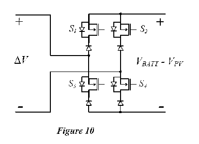
the unfolder in single-stage PV microinverters [1], as shown in Figure 9. The
unfolder can actively
invert AV in boost mode. The unfolder is realized by a bridge of four
bidirectional blocking
switches as shown in Figure 10.
Only two sets of switches are enabled in each mode: (S1, S4) in buck mode,
(S2, S3) in boost
mode. Given that AV changes sign very slowly based on irradiance and battery
voltage
fluctuations, the low-frequency unfolder only contributes to conduction
losses. It is therefore
recommended to use low Ron and low Vf devices. Moreover, the bridge provides
an additional
safety disconnect feature for the PV array, which is why it is connected on
the secondary side. The
complete PPP topology is shown in Figure 11.
The design procedure for the uk converter is well covered in the literature
[2] and not repeated
here. If AV is smaller then VBATT, the input current, voltage stress, and
inductor voltage swings
decrease in the converter. This allows the reduction or elimination of any
required snubbers in the
converter, use of smaller inductors, and higher FOM switches.
The transition between buck and boost modes is done by controlling the
unfolder bridge and active
switches simultaneously. In some embodiments, the active switches are turned
off simultaneously
with the unfolder. The energy stored in the inductor, Lsec is transferred to
both Csec and C0 UT
While this increases the voltage on the capacitors, the energy stored in the
inductor is much less
than that of the capacitors. The unfolder switches for the other mode are then
enabled to complete
the transition.
In boost mode, the full bridge converter of U.S. Patent 7,042,199 has six
active switches: Q1 to
Q4 and Q7, Q8; Q5 and Q6 are permanently on and do not contribute in the
operation. For the
full bridge to function, switches Q1 to Q4 impose a zero DC voltage square
waveform on the
primary side of the transformer with Q7 and Q8 conducting at different
intervals. During this
operation, there are six high frequency switches that are active. This differs
greatly from the
operation in the uk topology of the present invention, where only two high
frequency switches
8
CA 02946174 2016-10-18
WO 2015/172254
PCT/CA2015/050446
are active. A greater number of active switches degrades the converter
efficiency due to increased
switching and/or conduction losses; particularly when the topology is hard
switching. In addition,
the operation of the uk converter in the present invention does not require
four switching states as
the full bridge does in U.S. Patent 7,042,199; only two are sufficient due to
the presence of the
series capacitors on either side of the transformer. This increases the
reliability of the converter,
where the transformer is passively protected from saturation effects.
In buck mode, the full bridge converter of U.S. Patent 7,042,199 also has six
active switches: Q1
to Q4 and Q5, Q6; Q7 and Qg are permanently on and do not contribute in the
operation. For the
full bridge to function, switches Q5 to Q6 impose a zero DC voltage square
waveform on the
secondary side of the transformer. The primary side conducts either using
synchronous
rectification or through the use of MOSFET body diodes.
With the above in mind, there are a number of notable differences between the
embodiments of the
present invention and the prior art:
1. The partial power concept of the present invention is achieved by
feeding forward the input
bus to an unfolder as shown in Figure 9 whereas, in contrast, the prior art
connects the input
bus directly to the center tap of the transformer.
2. Embodiments of the present invention only use two active high frequency
switches for
buck and boost modes whereas the prior art uses six high frequency switches
for buck and
boost modes.
3. Switching between modes in the embodiments of the present invention is done
through the
unfolder, which effectively connects the input bus to the opposite terminal on
the
secondary side; this has the effect of reversing the power flow. The active
switches, Q1
and Q2, remain the active switches in both modes. In the prior art, the
switching of modes
is achieved by changing the active switches Q7, Qg which actively switch in
boost mode,
to Q5 and Q6, which now actively switch in buck mode. This is necessary since
the
full-bridge converter is not inherently bidirectional.
9
CA 02946174 2016-10-18
WO 2015/172254
PCT/CA2015/050446
4. The embodiments of the present invention utilize a simple two-winding
transformer
thereby obivating the need for a center-tapped transformer like US patent
7,042,199.
In addition, the embodiments of the present invention have been demonstrated
to work with high
efficiency at a switching frequency of 200 kHz using SiC power transistors
with clearly stated
mass and power density. The prior art has only demonstrated a switching
frequency of only 25 kHz
[3]; eight times less than the frequency of the embodiments of the present
invention. It is expected
that the listed efficiency in [3] will degrade at high frequency given the
number of active switches
in place.
The invention described herein is particularly useful in weight-sensitive
aeronautic or aerospace
applications although this invention may also be utilized in other
applications. In particular, this
invention is considered to be especially well-suited for solar-powered
aircraft such as the Solarship
designed and manufactured by Solar Ship Inc. of Toronto, Ontario, Canada. The
Solarship is
designed to operate in remote areas that have little or no fuel
infrastructure.
The Solarship aims to address the economic and logistical barriers that
prevent adequate supply
delivery to remote regions around the globe by (1) reducing the cost of
transport, (2) enabling
movement in-and-out of areas where other transport methods are ineffective due
to lack of fuel and
runways, and (3) ensuring cold chain storage and distribution. The Solarship
is a hybrid between a
bush plane and an airship. The added buoyancy from the helium-filled wing
increases the payload,
while the heavier-than-air design eliminates the need for expensive anchors.
One of the greatest advantages compared to standard aircraft is the ability to
land in a small area
the size of a soccer field. The simplified Solarship electrical architecture,
which is similar to
ground based Electric Vehicles (EVs), consists of a central battery pack,
electric motors driven by
inverters, and a set of dc-dc converters for performing Distributed Maximum
Power Point
Tracking (DMPPT) on the wing-mounted PV array as shown in Figure 13. A DMPPT
Partial
Power Processing (PPP) converter approach based on the invention described
herein is a
considerable improvement for this weight-sensitive aerospace application
because it reduces the
power rating of the dc-dc converter, and thus reduces the mass of heat sinks
and magnetic
CA 02946174 2016-10-18
WO 2015/172254
PCT/CA2015/050446
components.
Various modifications, refinements, alterations and variations to the
embodiments described
above may be implemented. For example, some contemplated modifications are as
follows:
1. The unfolder implementation may completely consist of active switches. This
is opposed
to one active switch and one passive switch as implemented in the embodiments
described
above. Using active bi-directional switches in the unfolder would reduce the
conduction
losses, which increasing the cost.
2. The concept of using an unfolder connected to an isolated bidirectional
topology is unique
and first proposed in this disclosure. The concept is particularly useful when
the ground
terminal of the battery bus and PV array must be connected together for safety
reasons. The
unfolder concept theoretically works with any isolated bidirectional topology
in order to
achieve the partial power concept and buck-boost operation.
3. The switch implementation in this disclosure can be MOSFETS or IGBTS or any
kind that
is capable of performing similar switching action. The concept is particularly
useful when
the ground terminal of the battery bus and PV array must be connected together
for safety
reasons.
4. Burst-mode control or any pulse frequency modulation scheme is possible for
this
converter under light load conditions to improve efficiency.
5. Maximum point power tracking (MPPT) of the PV panel may be achieved using
any
method suitable with duty cycle or current mode control.
6. It is possible to enable a pass-through mode that directly connects the PV
string the battery
bus via the unfolder bridge. This pass-through mode would reduce the losses
when the
battery and PV voltages are nearly identical.
11
CA 02946174 2016-10-18
WO 2015/172254
PCT/CA2015/050446
It is to be understood that the singular forms "a", "an" and "the" include
plural referents unless
the context clearly dictates otherwise. Thus, for example, reference to "a
device" includes
reference to one or more of such devices, i.e. that there is at least one
device. The terms
"comprising", "having", "including" and "containing" are to be construed as
open-ended terms
(i.e., meaning "including, but not limited to,") unless otherwise noted. All
methods described
herein can be performed in any suitable order unless otherwise indicated
herein or otherwise
clearly contradicted by context. The use of examples or exemplary language
(e.g. "such as") is
intended merely to better illustrate or describe embodiments of the invention
and is not
intended to limit the scope of the invention unless otherwise claimed.
The embodiments of the invention described above are intended to be exemplary
only. As
will be appreciated by those of ordinary skill in the art, to whom this
specification is addressed,
many other variations, modifications, and refinements can be made to the
embodiments
presented herein without departing from the inventive concept(s) disclosed
herein. The scope
of the exclusive right sought by the applicant(s) is therefore intended to be
limited solely by the
appended claims.
12