Note : Les descriptions sont présentées dans la langue officielle dans laquelle elles ont été soumises.
CA 02949267 2016-11-22
SYSTEMS AND METHODS FOR PROTECTING
AGAINST HIGH-RADIANT-FLUX LIGHT
BASED ON TIME-OF-FLIGHT
BACKGROUND
This disclosure generally relates to systems and methods for
the protection of imaging devices against light having a high radiant flux. As
used herein, the term "high-radiant-flux light" means light having any one or
more of the following measurable properties: high radial intensity (Mr), high
irradiance (W/m2) and high radiance (W-sr-1- m-2). Such high-radiant-flux
light
may be coherent (e.g., laser light) or incoherent..
A general problem is to achieve high probability of mission
success, at acceptably low cost, despite hazards. A hazard of increasing
concern is high-radiant-flux light, which can damage optical sensors
(hereinafter "image sensors") needed to (a) operate a vehicle safely or (b)
collect data, such as agricultural data or military surveillance data. This
hazard usually arises from lasers aimed at a vehicle. However, it may also
arise from arc welding equipment, exceptionally large or hot fires, a
lightning
bolt, or a nuclear blast.
Imaging devices, such as cameras and telescopes, are
especially vulnerable to high-radiant-flux light. By design, such imaging
devices use a lens or mirror to focus light onto an image sensor (such as a
focal plane array) comprising a multiplicity of pixels. This greatly increases
the
light intensity on pixels corresponding to the location of the high-radiant-
flux
light source in the image. Thus, light that is harmless to a structural
surface
may have damaging radiant flux at the image sensor. The high-radiant-flux
light can damage the image sensor by thermal shock, melting, or other
mechanisms.
One approach to solving this problem is using a laser sensor to
detect the presence of high-radiant-flux light in the imaging device's field
of
view. As used herein, the term "laser sensor" means a sensor that detects
1
CA 02949267 2016-11-22
high-radiant flux light (defined above). (For avoidance of doubt, it should be
noted that the term "laser sensor" as used herein does not mean a sensor
that detects laser light only or a sensor that detects all laser light.
Instead the
laser sensor detects any light having a radiant flux in excess of a specified
threshold, including but not limited to high-radiant-flux laser light.) The
laser
sensor transmits a signal via a signal line to a shutter inside the imaging
device. The shutter closes, blocking the light from reaching the image sensor
of the imaging device. This approach suffices for the weakest threats, such as
accidental exposure to lasers used in a light show, but it is insufficient for
the
more intense light commonly encountered in military situations due to reaction
time delays in such a system.
It would be advantageous to equip imaging devices with
protection systems that can block even the highest-intensity light before it
damages the image sensor.
SUMMARY
The subject matter disclosed in detail below is directed to
systems and methods for preventing high-radiant-flux light, such as laser
light
or a nuclear flash, from causing harm to imaging devices, such as a camera
or telescope. In response to detection of high-radiant-flux light, the
proposed
systems share the common feature that a shutter is closed sufficiently fast
that light from the source will be blocked from reaching the focal plane of
the
imaging device. Most of the proposed systems include a folded optical path to
increase the allowable reaction time for closing the shutter.
One aspect of the subject matter disclosed in detail below is an
imaging device comprising: a laser sensor configured to output an activation
signal in response to impingement thereon of light having a radiant flux
greater than a specified threshold; an image sensor comprising a multiplicity
of elements that convert impinging light to electrical signals; a first path-
bending optical component disposed along an optical path that extends from
a point in a vicinity of the laser sensor to the image sensor; a first shutter
2
CA 02949267 2016-11-22
disposed along a portion of the optical path that extends from the first path-
bending optical component to the image sensor; and a signal line connected
to carry the activation signal from the laser sensor to the first shutter. The
laser sensor, the signal line and the first shutter can be configured so that
in
response to some light and other light, both having a radiant flux greater
than
the specified threshold, concurrently arriving at the laser sensor and a
starting
point of the optical path respectively, the first shutter will become opaque
prior
to the other light impinging thereon in response to receipt of the activation
signal from the laser sensor via the signal line. The optical path is
configured
to produce a time-of-flight delay for light traveling from the vicinity of the
laser
sensor to the first shutter, and the laser sensor, the signal line, and the
first
shutter are configured to produce a shutter delay from the time a high-radiant-
flux arrives at the laser sensor to the time the first shutter becomes opaque,
wherein the time-of-flight delay is greater than the shutter delay. The
imaging
device may further comprise a second shutter disposed along a portion of the
optical path that extends from the first path-bending optical component to the
first shutter. In accordance with one embodiment, the first shutter comprises
an electro-optical shutter and the second shutter comprises a mechanical
shutter.
Another aspect of the subject matter disclosed in detail below is
an instrument comprising: a laser sensor configured to output an activation
signal in response to impingement thereon of light having a radiant flux
greater than a specified threshold; a first path-bending optical component
disposed along an optical path that extends from a point in a vicinity of the
laser sensor to a focal plane of the instrument; a shutter disposed along a
portion of the optical path that extends from the first path-bending optical
component to the focal plane; and a signal line connected to carry the
activation signal from the laser sensor to the shutter. The instrument may
further comprise second, third and fourth path-bending optical components,
wherein the second path-bending optical component is disposed along a
portion of the optical path that extends from the first path-bending optical
3
CA 02949267 2016-11-22
component to the focal plane, the third path-bending optical component is
disposed along a portion of the optical path that extends from the second
path-bending optical component to the focal plane, and the fourth path-
bending optical component is disposed along a portion of the optical path that
extends from the third path-bending optical component to the focal plane.
A further aspect is an imaging device comprising: a laser sensor
configured to output an activation signal in response to impingement thereon
of light having a radiant flux greater than a specified threshold; an image
sensor comprising a multiplicity of elements that convert impinging light to
electrical signals; means for increasing a time-of-flight of light along an
optical
path that extends from a point in a vicinity of the laser sensor to the image
sensor; a shutter disposed along a portion of the optical path that extends
from the volume of substance having a high index of refraction to the image
sensor; and a signal line connected to carry the activation signal from the
laser sensor to the first shutter. In some embodiments, the structure that
performs the function of increasing a time-of-flight of light along an optical
path comprises a volume of substance having a high index of refraction. In
other embodiments, the structure that performs the function of increasing a
time-of-flight of light along an optical path comprise one or more reflective
surfaces.
Yet another aspect of the subject matter disclosed below is a
method comprising: (a) detecting a radiant flux entering an optical instrument
that has above a specified threshold; (b) when the specified threshold is
reached or exceeded, sending an activation signal via a signal line to a
shutter disposed inside the optical instrument; (c) delaying the arrival of
the
entering light at a shutter inside the optical instrument by an amount of time
equal to a time-of-flight delay; and (d) in response to sending of the
activation
signal, the shutter becomes opaque at a time which is subsequent to a time
when step (a) occurs by a total shutter delay, wherein the time-of-flight
delay
is greater than the total shutter delay.
4
Yet another aspect of the subject matter disclosed below is an
imaging device comprising: a laser sensor configured to output an activation
signal in response to impingement thereon of light having a radiant flux
greater than a specified threshold; an image sensor comprising a multiplicity
of elements that convert impinging light to electrical signals; a first path-
bending optical component disposed along an optical path that extends from
a point in a vicinity of said laser sensor to said image sensor; a first
shutter
disposed along a portion of said optical path that extends from said first
path-
bending optical component to said image sensor; a second shutter disposed
along a portion of said optical path that extends from said first path-bending
optical component to said first shutter; and a signal line connected to carry
said activation signal from said laser sensor to said first shutter.
Yet another aspect of the subject matter disclosed below is an
instrument comprising: a laser sensor configured to output an activation
signal in response to impingement thereon of light having a radiant flux
greater than a specified threshold; a first path-bending optical component
disposed along an optical path that extends from a point in a vicinity of said
laser sensor to a focal plane of the instrument; a first shutter disposed
along a
portion of said optical path that extends from said first path-bending optical
component to said focal plane; a second shutter disposed along a portion of
said optical path that extends from said first path-bending optical component
to said first shutter; and a signal line connected to carry said activation
signal
from said laser sensor to said shutter.
4a
Date Recue/Date Received 2020-10-08
Yet another aspect of the subject matter disclosed below is an
imaging device comprising: a laser sensor configured to output an activation
signal in response to impingement thereon of light having a radiant flux
greater than a specified threshold; an image sensor comprising a multiplicity
of elements that convert impinging light to electrical signals; means for
increasing a time-of-flight of light along an optical path that extends from a
point in a vicinity of said laser sensor to said image sensor; a first shutter
disposed along a portion of said optical path that extends from said means for
increasing the time-of-flight of light to said image sensor; a second shutter
disposed along a portion of said optical path that extends from said means for
increasing the time-of-flight of light to said first shutter; and a signal
line
connected to carry said activation signal from said laser sensor to said first
shutter.
4b
Date Recue/Date Received 2020-10-08
CA 02949267 2016-11-22
Other aspects of systems and methods for the protection of
imaging devices against high-radiant-flux light are disclosed below.
BRIEF DESCRIPTION OF THE DRAWINGS
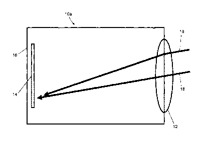
FIG. 1 is a diagram representing an imaging device that is
focusing incoming light onto a focal plane, thereby increasing the light's
intensity.
FIG. 2 is a diagram representing an imaging device equipped
with a shutter that can be activated to close when high-radiant-flux light is
detected by a laser sensor.
FIG. 3A is a graph of light intensity at a focal plane of an
imaging device versus time for two laser attacks of differing intensities I
and
'2.
FIG. 3B is a graph of temperature at a focal plane of an imaging
device versus time for two laser attacks that would produce the respective
intensity profiles depicted in FIG. 3A.
FIG. 4 is a diagram depicting structural and functional aspects
of an imaging device equipped with a protection system having one shutter in
accordance with a first embodiment.
FIG. 5 is a diagram depicting structural and functional aspects
of an imaging device equipped with a protection system having a slower
mechanical shutter "upstream" from a faster electro-optical shutter in
accordance with a second embodiment.
FIG. 6 is a graph of temperature at the focal plane versus time
for the imaging device depicted in FIG. 5.
FIG. 7 is a diagram depicting structural and functional aspects
of a telescope having a Cassegrain reflector, which telescope is further
5
CA 02949267 2016-11-22
equipped with a protection system having a shutter near the secondary mirror
in accordance with a third embodiment.
FIG. 8 is a diagram depicting structural and functional aspects
of a telescope having a Cassegrain reflector, which telescope is further
equipped with a protection system having a shutter behind the primary mirror
in accordance with a fourth embodiment.
FIG. 9 is a diagram depicting structural and functional aspects
of a Newtonian telescope equipped with a protection system having a shutter
near the laser sensor in accordance with a fifth embodiment.
FIG. 10 is a diagram depicting structural and functional aspects
of an imaging device equipped with a protection system having a shutter in
accordance with a sixth embodiment in which multiple path-bending optics
create a very long optical path.
FIG. 11 is a diagram depicting structural and functional aspects
of an imaging device equipped with a protection system having a shutter in
accordance with a seventh embodiment in which the optical path is effectively
lengthened by a substance with high index of refraction.
FIG. 12 is a diagram depicting structural and functional aspects
of a periscope equipped with a protection system having a shutter and an
extended optical path in accordance with an eighth embodiment.
Reference will hereinafter be made to the drawings in which
similar elements in different drawings bear the same reference numerals.
DETAILED DESCRIPTION
Illustrative embodiments of a protection system are described in
some detail below. However, not all features of an actual implementation are
described in this specification. A person skilled in the art will appreciate
that in
the development of any such actual embodiment, numerous implementation-
specific decisions must be made to achieve the developer's specific goals,
6
CA 02949267 2016-11-22
such as compliance with system-related and business-related constraints,
which will vary from one implementation to another. Moreover, it will be
appreciated that such a development effort might be complex and time-
consuming, but would nevertheless be a routine undertaking for those of
ordinary skill in the art having the benefit of this disclosure.
By design, an imaging device uses a lens or mirror to focus light
onto an image sensor. FIG. 1 depicts an imaging device 10a that has a lens
12, an image sensor 14, and a housing 16. The housing 16 has an aperture
through which incident light propagates on its way to the focal plane of the
imaging device 10a. The arrows in FIG. 1 indicate optical paths 18 of
respective incoming light rays 18 that are being focused by the lens 12 onto a
portion of the image sensor 14, thereby increasing the light's intensity.
(Other
light rays are not shown to avoid clutter in the drawing.) This greatly
increases
the intensity on pixels corresponding to the location of the high-radiant-flux
light source in the image. Thus, light that is harmless to a structural
surface
may have damaging intensity at the image sensor 14.
One approach to solving this problem is depicted in FIG. 2,
which shows an imaging device 10b that has a lens 12, an image sensor 14,
a laser sensor 20, and a shutter 22, all of which components may be attached
directly or indirectly (by support means not shown) to a housing 16. The laser
sensor 20 detects the presence of high-radiant-flux light in the imaging
device's field of view. The laser sensor 20 transmits an activation signal via
a
signal line 24 to the shutter 22 when high-radiant-flux light is detected. In
response to receipt of that activation signal, the shutter 22 becomes opaque,
thereby blocking at least some of the incoming light from reaching the image
sensor 14 disposed at the focal plane of the imaging device 10b.
The approach depicted in FIG. 2 may be insufficient for blocking
the intense light commonly encountered in military situations. The reason for
this insufficiency lies in the following three delays: (1) the laser sensor
response time At
-- sensor (any laser sensor requires a non-zero time to detect the
7
CA 02949267 2016-11-22
arrival of high-radiant-flux light and send a signal); (2) the signal transit
time
Attransit (the signal must travel from the laser sensor 20 to the shutter 22;
it
cannot travel faster than the speed of light, 0.3 meter per nanosecond); and
(3) the shutter response time Atresponse (no shutter can close instantly; it
requires a nonzero reaction time to become opaque after a signal arrives; the
shorter the reaction time, the more costly the shutter). These delays can be
summed to produce a single value Atshutter, which is the total shutter delay
from when high-radiant-flux light arrives at the laser sensor 20 to when the
shutter 22 becomes opaque.
FIG. 3A is a graph of light intensity at an image sensor versus
time for two laser attacks of differing intensities I and L. FIG. 3B is a
graph
of temperature at the same image sensor versus time for the same laser
attacks.
The plot labeled I in FIG. 3A represents a relatively low-
intensity attack beginning at time to. The plot labeled Ti(t) in FIG. 3B
represents the corresponding temperature at the focal plane. Starting at to,
the temperature rises from an initial value To toward the damage threshold
'damage- Before it reaches that threshold, the shutter 22 closes at time
tch,õ.
The temperature stops rising, and the image sensor 14 survives.
The plot labeled 12 in FIG. 3A represents a higher-intensity
attack. The plot labeled T2(t) in FIG. 38 represents the corresponding
temperature at the focal plane. As above, the temperature rises from the
initial value To, but given the higher intensity L, the temperature rises
faster
than in the weak attack. The temperature exceeds the damage threshold
Tdamage before the shutter 22 closes at tdose. In this event, the image sensor
14
may be damaged or destroyed. In contrast, the protection systems described
in detail below can block even the highest-intensity light before it damages
the focal plane.
8
CA 02949267 2016-11-22
FIG. 4 depicts structural and functional aspects of an imaging
device 10c equipped with a protection system in accordance with a first
embodiment. The imaging device 10c comprises the following elements: a
lens 12 (or other image-forming optics), an image sensor 14 (or other image
sensor); a mirror 28 (or other path-bending optic(s); a laser sensor 20; a
shutter 22 (electro-optical, mechanical, etc.); a signal line 24 (a wire,
coaxial
cable, or optical fiber); a housing 16a having an aperture; and a baffle 26.
As
shown in FIG. 4, the mirror 28 reflects light from the lens 12 onto the image
sensor 14. The shutter 22, when closed, blocks the light's path to protect the
image sensor 14. The optical path length from a point near the laser sensor
to the shutter 22 via the mirror 28 is much longer than the length of the
signal line 24 from the laser sensor 20 to the shutter 22. The elongated
housing 16a surrounds and protects the components and the optical path.
Baffle 26 blocks any light scattered by diffraction, dust or other blemishes
on
15 lens 12 from reaching shutter 22 via any path with an optical path
length less
than the optical path length from a point near the laser sensor 20 to the
shutter 22 via the mirror 28
In accordance with the embodiment depicted in FIG. 4, the
process for protecting the imaging device 10c from incoming high-radiant-flux
20 light includes the following major steps:
(1) The laser sensor 20 (placed near the aperture) detects light
having a radiant flux above a specified threshold.
(2) When the specified threshold is reached or exceeded, the
laser sensor 20 sends an activation signal (electrical or optical) via the
signal
line 24 to the shutter 22.
(3) Meanwhile, the high-radiant-flux light travels by a long optical
path through the housing 16a. A first portion 18a of that optical path
(indicated by a first arrow in FIG. 4 and having a length Asi) extends from a
point in the vicinity of the laser sensor 20 to the mirror 28; a second
portion
9
CA 02949267 2016-11-22
18b of that optical path (indicated by a second arrow in FIG. 4 and having a
length As2) extends from the mirror 28 to the shutter 22.
(4) In response to receipt of the activation signal from the laser
sensor 20, the shutter 22 becomes opaque.
(5) When the high-radiant-flux light reaches the shutter 22 (now
in an opaque state), enough of the incident light can be blocked to prevent
damage to the image sensor 14.
(6) The laser sensor 20 detects a return to light levels below the
specified threshold and sends a de-activation signal which causes the shutter
22 to open (i.e., become transparent).
In operation, the optical path length As is long enough to impose
a time-of-flight delay As/c, where c is the speed of light, and this time-of-
flight
delay is greater than the total shutter delay Atshutter. That is,
As/c> Atshutter (1)
For a two-legged optical path as shown in FIG. 4, and showing all elements of
Atshutter, this equation becomes:
(Ast As2)/c > Atsensor Attransit Atresponse (2)
where Asi is the optical path length from a point in the vicinity of the laser
sensor 20 to the mirror 28, and As2 is the optical path length from the mirror
28 to the shutter 22.
The common elements of the various imaging devices disclosed
herein will be described more generally in the following individually entitled
sub-sections.
Imace Sensor
The image sensor 14 may comprise a staring focal plane array
that includes a multiplicity of elements that convert impinging light to
electrical
CA 02949267 2016-11-22
signals, such as a charge coupled device (CCD) sensitive to visible or
infrared
wavelengths. In the alternative, it can be a single-pixel camera (compressive
imaging system), an imaging photomultiplier, a vidicon tube, a photochemical
film, or others.
Image-Forming Optics
The image-forming optics may comprise a lens, a mirror, or a
combination thereof that focuses light on the image sensor to create an
image. It may be a single optical element such as the lens 12 shown in
FIG. 4, or a multi-element system such as an achromatic lens, a Newtonian
mirror system, or a Schmidt¨Cassegrain lens¨mirror combination.
Path-Bending Optics
The path-bending optics may comprise an optical element, such
as a mirror 28, that changes the direction of light. Preferably, the direction
is
changed by at least 900. This includes light that forms the image and light
that
can damage the image sensor. Changing the light's direction allows the path
length of the light to be much greater than the path length for the shutter
signal. Besides a single flat mirror 28 as shown in FIG. 4, this optical
element
may be a reflecting prism, multiple mirrors, or combinations thereof. In some
embodiments (described n more detail later), the mirror is curved and is part
of the image-forming optics.
Laser Sensor
The laser sensor is a photosensitive electronic device that has
roughly the same field of view as the imaging device. When a sufficiently
high-radiant-flux light appears in its field of view, the laser sensor
transmits a
signal quickly¨typically in less than a nanosecond. As seen in FIG. 4,
preferably the laser sensor 20 is positioned near the shutter 22 so the signal
line 24 from the laser sensor 20 to the shutter 22 will be short. The laser
sensor 20 is typically much less sensitive than the image sensor 14, as it
only
needs to respond to high-radiant-flux light. It can also survive exposure to
light having a higher radiant energy than what the image sensor 14 can be
11
CA 02949267 2016-11-22
exposed to. A typical laser sensor comprises a processor having a
thresholding function, a photodetector, and a lens or other focusing element
to provide directionality.
Shutter
The shutter 22 is a device that has two states. In one state, the
shutter 22 at least partially blocks the passage of light. In the other state,
the
shutter 22 allows the passage of light. The shutter 22 may comprise crossed
polarizers surrounding a fast-acting magneto-optical or electro-optical device
such as a Pockels cell, a Kerr cell, a Faraday modulator, or an active-matrix
liquid-crystal grid (similar to the technology used in liquid crystal
displays). To
give the shutter 22 as much time as possible to receive the activation signal
and to respond, the shutter 22 is typically adjacent to the image sensor 14
and as close as possible to the laser sensor 20.
Signal Line
As depicted in FIG. 4, the signal line 24 carries a signal from the
laser sensor 20 to the shutter 22. The signal line 24 is configured to take as
direct a route as possible from laser sensor 20 to shutter 22. For an optical
signal, the signal line 24 may be optical fiber (signal speed ¨2 x 10⁸ m/s),
or it
may be a free-space path (perhaps shielded by a hollow tube) along which
the signal moves at 3 x 10⁸ m/s. For an electrical signal, the signal line 24
is
configured to have minimal inductance and capacitance per unit length to
achieve the highest possible signal speed.
Housing
Time must be given for the shutter 22 to receive the activation
signal from the laser sensor 20 and to change state. Elongating the path that
the light takes to reach the image sensor 14 allows this to occur. There are
multiple housing designs which can be used. The key element is the distance
the light must travel versus the distance the signal must travel. At 0.3 meter
per nanosecond, a two-meter path gives six nanoseconds of delay. The
housing 16a shown in FIG. 4 could be designed to achieve a two-meter path
12
CA 02949267 2016-11-22
in one meter of length by positioning the mirror 28 one meter from each of the
laser sensor 20 and the shutter 22.
Alternative embodiments of imaging devices equipped with
protection systems will now be described in detail for the purpose of
illustrating manifold ways in which the concept disclosed herein may be
reduced to practice.
In some alternative embodiments, there is a second shutter
which is mechanical. A mechanical shutter is too slow to act before the high-
radiant-flux light reaches the image sensor, but once closed, it blocks 100%
of the light. Affordable electro-optical shutters typically do not block 100%
of
the light, so some alternative embodiments use both types of shutters in
tandem: the electro-optical shutter acts quickly to block most of the light,
and
the mechanical shutter subsequently blocks the rest of light.
FIG. 5 depicts structural and functional aspects of an imaging
device 10d equipped with a protection system in accordance with a second
embodiment. In this embodiment, the protection system comprises a slower
mechanical shutter 22a "upstream" from a faster electro-optical shutter 22b.
The mechanical shutter 22a is tougher (i.e., more rugged) than the electro-
optical shutter 22b, so as shown in FIG. 5, the mechanical shutter 22a is
positioned to protect the weaker, more costly electro-optical shutter 22b from
prolonged exposure to high-radiant-flux light.
FIG. 6 shows how adding a mechanical shutter 22a helps
protect the image sensor 14. (The signal line from the laser sensor 20 to the
mechanical shutter 22a is not shown to avoid clutter in the drawing.) Given
that the total shutter delay for the electro-optical shutter 22b is
Atshutter_l, the
electro-optical shutter 22b closes at time tek,s, 1, but since it does not
block
100% of the light, the temperature of the image sensor 14 (or other image
sensor) continues to rise slowly. Given that the total shutter delay
Atshutter_2 for
the mechanical shutter 22a is longer than the total shutter delay Atshutter_i
for
13
CA 02949267 2016-11-22
the electro-optical shutter 22b, the mechanical shutter 22a closes at time
tcl0se_2, which is later than the time tdõõ 'when the electro-optical shutter
22b
closed. The closed mechanical shutter blocks 100% of light, so that the
temperature at the image sensor 14 (or other image sensor) rises no further
(i.e., does not reach the temperature Tdamage at which damage might occur).
Many imaging systems use a Cassegrain optical configuration.
A Cassegrain reflector is a combination of a concave primary mirror and a
convex secondary mirror, often used in optical telescopes. In a symmetrical
Cassegrain reflector, both mirrors are aligned about the optical axis, and the
primary mirror usually contains a hole in the centre, thus permitting the
light to
reach an eyepiece, a camera, or a light detector. FIG. 7 depicts structural
and
functional aspects of a Cassegrain imaging device be (e.g., a telescope
having a Cassegrain reflector) equipped with a protection system having a
shutter 22 near the secondary mirror 32. FIG. 7 shows use of the Cassegrain
primary mirror 30 as both a path-bending optical element and an image-
forming optical element. The incoming light rays travel by respective long
optical paths through the housing 16b. A first portion 18a of respective
optical
paths for two light rays extends from a point in the vicinity of the laser
sensor
to the primary mirror 30; a second portion 18b of the respective optical
20 paths for the two light rays extends from the primary mirror 30 to the
secondary mirror 32; and a third portion 18c of the respective optical paths
for
the two light rays extends from the secondary mirror 32 to the image sensor
14.
A benefit of the embodiment depicted in FIG. 7 is that light
passes through the shutter 22 twice on its way to the image sensor 14. This
increases the effective opacity of the shutter 22: a shutter 22 that blocks
90%
of the light in a single pass blocks 99% of the light in a double pass. This
allows an inexpensive shutter to work as well as a more expensive one.
A disadvantage of the embodiment depicted in FIG. 7 is that
hardware around the shutter 22 may block some light, reducing the
14
CA 02949267 2016-11-22
performance of the telescope. FIG. 8 depicts an alternative that avoids this
disadvantage. In this embodiment, a Cassegrain imaging device 10f is
equipped with a protection system having a shutter 22 disposed behind the
primary mirror 30 and in front of the image sensor 14. Placing the shutter 22
behind the primary mirror 30 puts the extra shutter hardware out of the
optical
path. In some applications, this may be preferable despite losing the double-
pass advantage provided by the embodiment depicted in FIG. 7.
FIG. 9 depicts structural and functional aspects of a Newtonian
imaging device lOg (e.g., a Newtonian telescope) equipped with a protection
system having a shutter 22 near the laser sensor 20 in accordance with a
further embodiment. Incoming light is reflected and focused by a concave
primary mirror 30 onto a flat diagonal secondary mirror 32a the latter in turn
reflects the focused beam onto the image sensor 14. This optical
configuration places the shutter 22 behind an aperture in the housing 16c and
very close to the laser sensor 20 and keeps the extra shutter hardware out of
the optical path.
FIG. 10 depicts structural and functional aspects of an imaging
device 10h equipped with a protection system having a shutter 22 in
accordance with an alternative embodiment in which multiple path-bending
optics create a very long optical path. The imaging device 10h comprises the
following elements: a lens 12, an image sensor 14, mirrors 28a and 28b, a
laser sensor 20, a shutter 22, a signal line 24, a housing 16d having an
aperture, and a pair of baffles 26a and 26b. As indicated by arrows in FIG. 4,
the first mirror 28a reflects light from the lens 12 onto the mirror 28b; the
mirror 28b reflects light from mirror 28a back onto mirror 28a; and the mirror
28a reflects light from mirror 28b toward the shutter 22. The shutter 22, when
opaque, at least partially blocks the light's path to protect the image sensor
14. The optical path length from a point near the laser sensor 20 to the
shutter 22 is much longer than the length of the signal line 24 from the laser
sensor 20 to the shutter 22. More specifically, the incoming laser light
travels
CA 02949267 2016-11-22
by a long optical path through the housing 16d. A first portion 18a of that
optical path (indicated by a first arrow in FIG. 10) extends from a point in
the
vicinity of the laser sensor 20 to the mirror 28a; a second portion 18b of
that
optical path (indicated by a second arrow) extends from the mirror 28a to the
mirror 28h; a third portion 18c of that optical path (indicated by a third
arrow)
extends from the mirror 28b to the mirror 28a; and finally a fourth portion
18d
of that optical path (indicated by a fourth arrow) extends from the mirror 28a
to the shutter 22.
In the embodiments depicted in FIGS. 4, 5 and 7-9, the imaging
device has one or two major bends in the optical path. The embodiment
depicted in FIG. 10 use multiple path-bending optics to create very long
optical paths in limited physical space. For simplicity of illustration, the
version
shown here keeps the optical path roughly in a single plane and has non-
crossing legs in the optical paths. More complicated embodiments minimize
the device's volume by having optical path legs that cross, e.g., in a star
pattern or a three-dimensional mesh. Multiple reflecting surfaces can
introduce substantial optical errors, so some embodiments use adaptive
optics between the shutter and the image sensor to correct any errors.
In the previously described embodiments, the apparatus
included a folded optical path. Another way to delay the arrival of high-
radiant-flux light at an image sensor is to use a substance having a high
index
of refraction to delay the time-of-flight.
FIG. 11 depicts structural and functional aspects of an imaging
device 10i in accordance with a further alternative embodiment. In this
configuration, a portion of the optical path 18 is filled with a transparent
substance 34 (solid, liquid, or gas) that has a high index of refraction n.
That
is, the speed of light in the material is slowed by a factor of, say, 1.33
(water)
to as much as 4.0 (germanium, used in long-wave infrared imagers) or higher
(exotic substances such as Bose¨Einstein condensate). Thus the optical path
is effectively lengthened by the high-index substance 34 disposed inside the
16
CA 02949267 2016-11-22
housing 16e. Signals propagating along the signal line 24 are not slowed, so
they can travel as fast as the speed of light in vacuum. Given an optical path
of sufficient length, the activation signal reaches the shutter 22 well in
advance of the high-radiant-flux light. The shutter 22 becomes opaque (i.e.,
closes) before the light reaches it whenever the following relation is true:
nAslc> Atshutter (3)
More generally, the optical path may comprise multiple legs,
each leg i having length As and index of refraction ni. In this case, the
appropriate relation is:
(En,As, )/ c > Atshõõõ (4)
where E denotes a sum over all legs.
Some embodiments can use both a folded optical path and a
path that is at least partially filled with a high-index substance. In
addition,
when a path-bending element is a prism, the refractive index of the prism is
at
least 1.3, so light traveling through it incurs a substantial delay. In some
embodiments, the prism is designed to have a large internal path length and
to incorporate material with unusually high index of refraction.
The embodiments described above each have a shutter
between the image-forming optics and the image sensor. In some
embodiments, typically those where the image-forming optics have a short
focal length, the image-forming optics may be between the shutter and the
image sensor (i.e., "downstream" of the shutter). The path-bending optics and
the laser sensor would remain "upstream" of the shutter.
A special case of putting the image-forming optics
"downstream" of the shutter is an embodiment that protects a human
observer, i.e., the image-forming optics and the image sensor are both part of
a human eye. Prior art includes many forms of periscope: those used in
submarines, in armored turrets on tanks, fortresses, and naval vessels, in
17
CA 02949267 2016-11-22
trench warfare, and in covert surveillance by police. FIG. 12 is a diagram
depicting structural and functional aspects of a periscope 8 equipped with a
protection system having a shutter 22 placed in front of the eye of a human
observer 6 and further having an extended optical path. The extended optical
path through the periscope 8 allows shutter 22 to close before high-radiant-
flux light reaches the eye of the human observer 6.
In the embodiment depicted in FIG. 12, the regular periscope
structure is extended below the viewer's eye to increase the optical path.
(Other parts of the periscope optics are omitted for clarity.) This longer
path
allows the signal from the laser sensor 20 to reach the shutter 22 before the
high-radiant-flux light reaches the shutter 22. A first portion 18a of that
optical
path (indicated by a first arrow in FIG. 12) extends from a point in the
vicinity
of the laser sensor 20 to the mirror 36; a second portion 18b of that optical
path (indicated by a second arrow) extends from the mirror 36 to a first facet
of a prism 38; a third portion 18c of that optical path (indicated by a third
arrow) extends from the first facet of prism 38 to a second facet of prism 38;
and finally a fourth portion 18d of that optical path (indicated by a fourth
arrow) extends from the mirror 28a to the shutter 22.
In other embodiments (not shown), the forward opening of the
periscope can be at the same height as the human observer. In these
embodiments, the point is not to see over an obstacle, but rather simply to
protect the observer's eyes from high-radiant-flux laser light or other high-
radiant-flux light.
Alternative criteria for shutter closure may be employed. The
activation threshold may be based on radiant intensity (e.g., watts per
steradian), irradiance (e.g., watts per square meter), or radiance(e.g., watts
per steradian per square meter). Slightly different laser sensors can be
employed depending on whether radiance or irradiance is being detected. To
detect irradiance, the laser sensor may comprise a single photodetector. To
detect radiance, the laser sensor should comprise a focusing element, a
18
CA 02949267 2016-11-22
photosensitive chip with multiple pixels, and a processor that issues the
activation signal when the amount of light on one pixel exceeds the threshold.
While imaging devices and instruments having means for laser
protection have been described with reference to various embodiments, it will
be understood by those skilled in the art that various changes may be made
and equivalents may be substituted for elements thereof without departing
from the teachings herein. In addition, many modifications may be made to
adapt the concepts and reductions to practice disclosed herein to a particular
situation. Accordingly, it is intended that the subject matter covered by the
claims not be limited to the disclosed embodiments.
The process claims set forth hereinafter should not be
construed to require that the steps recited therein be performed in
alphabetical order (any alphabetical ordering in the claims is used solely for
the purpose of referencing previously recited steps) or in the order in which
they are recited. Nor should they be construed to exclude any portions of two
or more steps being performed concurrently or alternatingly.
19