Note : Les descriptions sont présentées dans la langue officielle dans laquelle elles ont été soumises.
1
APPARATUSES AND METHODS FOR DETERMINING ANALYTE CHARGE
[0001]
STATEMENT AS TO FEDERALLY SPONSORED RESEARCH
[0002] This invention was made with the support of the United States
government under Contract
number NIH P01 HG000205 by the National Institutes of Health (NIH).
BACKGROUND
[0003] There is a great deal of interest in the field of biotechnology on
nucleic acid sensors that
can replace the currently popular optics-based biosensors. While there has
been numerous
theoretical advances in nucleic acids research, the cost of performing the
methods developed
(whether for diagnosis of a patient's ailment or investigation of a pathogenic
trait) frequently
hamper their adoption into clinical settings. For example, while the cost of
human genome
sequencing has been dramatically reduced from $3 billion to $20 thousand, it
is still far too
expensive to be used in a routine clinical environment. The optics-based
sensing (that tends to be
time consuming to operate, needs modified fluorescing reagents, requires bulky
optical sources and
needs costly imaging equipment) is seen as a major bottleneck in lowering the
cost of genomics.
While the integrated electrical sensors seem to provide many advantages over
the optical ones,
recent approaches either have limitations in manufacturability or have shown
poor robustness.
SUMMARY
[0004] Recognized herein is the need for improved sensors for detecting
analytes such as nucleic
acids (e.g., that are more sensitive, more robust, and/or more easily
manufactured). In various
aspects, the present disclosure provides such sensors and methods for using
the sensors, for
example, to sequence a nucleic acid molecule.
Date Recue/Date Received 2022-09-30
2
100051 Various aspects of the present disclosure are directed toward a sensor
for detecting a
charged analyte and methods of using the sensor.
[0005a1 Accordingly, there is described a sensor for detecting a charged
analyte, the sensor
comprising: a fluidic chamber having electrically opposing portions with a
membrane between, the
membrane providing a pore suitable for the passage of an electrolyte between
the electrically
opposing portions of the fluidic chamber, and having at least one charged
analyte tethered in
proximity to the pore; a first circuit configured to apply an electric field
capable of passing the
electrolyte through the pore and pulling the at least one charged analyte into
the pore, wherein the
electric field has a strength of at least 105 Volts per meter, and wherein the
membrane and a wall
of the pore are surrounded by an electrical double layer (EDL), and wherein
the electric field having
the strength of at least 105 Volts per meter is configured to de-screen the
EDL; and a second circuit
configured to measure a signal indicative of the charge of the at least one
charged analyte upon at
least one charged analyte being pulled into the pore.
100061 The second circuit optionally includes a sensing electrode for
measuring the signal,
wherein the sensing electrode is located at a distance away from the at least
one charged analyte.
The distance may be at least 2-times a Debye length associated with the at
least one charged analyte.
¨
The Debye length is calculated using the Debye-Hiickel equation: AD VcIcT IC
, wherein AD =
Debye length, c= electric constant, k = Boltzman constant, T = temperature,
and Co = ionic
concentration. In various embodiments, respective sizes or diameters (and/or
shapes) of the pore
can vary as needed to pass certain types (having corresponding sizes) of
charged analytes. As one
example, certain charged analytes may be appropriate for pores sized between
25 nm and 2000 nm
in diameter as used with a membrane having a thickness between 50 nm and 3 gm.
For other
analytes such as smaller-sized analytes, the pore has a diameter of at least
about 10 nanometers
Date Recue/Date Received 2022-09-30
3
(nm). The electric field may be capable of generating a non-equilibrium
transport condition. The
membrane may be electrically insulating. Further, the membrane may be
comprised of graphene,
alumina (A1203), silicon dioxide (SiO2) or silicon nitride (S13N4) (e.g.,
which are and/or can be
electrically insulating material). The first circuit may include a first
electrode in a first electrically
opposing portion (e.g., the top portion) of the fluidic chamber and a second
electrode in a second
electrically opposing portions (e.g., the bottom portion) of the fluidic
chamber. The second circuit
may include an electrode embedded in the membrane in proximity to the pore.
The second circuit
may include an amplifier capable of amplifying the signal. The amplifier may
be within about 5000
gm from the pore. The signal may be linearly proportional to the charge of the
at least one charged
analyte. The at least one charged analyte may be a nucleic acid molecule.
Further, the at least one
charged analyte may have a net charge of at least about 40 e-. However, the at
least one charged
analyte may have a net charge lower or higher than about 40 e-. The
electrolyte may have an ionic
strength of about 1001tM to about 1M. Further, the at least one charged
analyte can be tethered in
proximity to the pore by a molecular structure and/or be being immobilized.
Further, the sensor
may have a plurality of pores into which the plurality of charged analytes are
pulled. Further, the
plurality of charged analytes may be clonal. In another aspect, a device is
disclosed in which the
device has a plurality of the sensors detailed herein.
100071 There is also described a kit for detecting a charged analyte, the kit
comprising: at least
one charged analyte; and a sensor including: a fluidic chamber having
electrically opposing
portions with a membrane between, the membrane providing a pore suitable for
the passage of an
electrolyte between the electrically opposing portions of the fluidic chamber,
and having the at least
one charged analyte tethered in proximity to the pore, wherein the electric
field has a strength of at
least 105 Volts per meter, and wherein the membrane and a wall of the pore are
surrounded by an
Date Recue/Date Received 2022-09-30
4
electrical double layer (EDL), and wherein the electric field having the
strength of at least 105 Volts
per meter is configured to de-screen the EDL; a first circuit configured to
apply an electric field
capable of passing the electrolyte through the pore and pulling the at least
one charged analyte into
the pore; and a second circuit configured to measure a signal indicative of
the charge of the at least
one charged analyte upon at least one charged analyte being pulled into the
pore. The membrane
may be electrically insulating. Further, the membrane may be comprised of
graphene, alumina
(A1203), silicon dioxide (SiO2) or silicon nitride (Si3N4). The first circuit
may include a first
electrode in a first electrically opposing portion (e.g., the top portion) of
the fluidic chamber and a
second electrode in the second electrically opposing portion (e.g., the bottom
portion) of the fluidic
chamber. The second circuit may include an electrode embedded in the membrane
in proximity to
the pore. The second circuit may include an amplifier capable of amplifying
the signal. The
amplifier may be within about 5000 um from the pore. The signal may be
linearly proportional to
the charge of the at least one charged analyte. The at least one charged
analyte may be a nucleic
acid molecule. Further, the at least one charged analyte may have a net charge
of at least about 40
e-. However, the at least one charged analyte may have a net charge lower or
higher than about 40
e-. The electrolyte may have an ionic strength of about 100uM to about 1M.
Further, the sensor
may have a plurality of pores into which the plurality of charged analytes are
pulled. Further, the
plurality of charged analytes may be clonal.
[0008] In accordance with other related embodiments, there is described a
method for detecting a
charged analyte, the method comprising: providing a fluidic chamber having
electrically opposing
portions with a membrane between, one of the electrically opposing portions
having an electrolyte,
the membrane providing a pore suitable for the passage of the electrolyte
between the electrically
opposing portions of the fluidic chamber, and having at least one charged
analyte tethered in
Date Recue/Date Received 2022-09-30
5
proximity to the pore; applying an electric field to pass the electrolyte
through the pore and pull the
at least one charged analyte into the pore, wherein the electric field has a
strength of at least 105
Volts per meter, and wherein the membrane and a wall of the pore are
surrounded by an electrical
double layer (EDL), and wherein the electric field having the strength of at
least 105 Volts per meter
is configured to de-screen the EDL; and measuring a signal indicative of the
charge of the at least
one charged analyte upon the at least one charged analyte being pulled into
the pore. The method
optionally includes the at least one charged analyte being pulled to a
position in proximity to a
periphery of the pore. In this method, the first circuit may apply the
electric field. The second circuit
may measure the signal.
[0009] Another related aspect of the disclosure is directed to a method that
includes providing a
fluidic chamber having electrically opposing portions (e.g., a top portion and
a bottom portion)
between a membrane (e.g., separated by a membrane), where one of the
electrically opposing
portions (e.g., the top portion) includes an electrolyte, the membrane
providing a pore suitable for
the passage of an electrolyte between the electrically opposing portions
(e.g., from the top portion
to the bottom portion) of the fluidic chamber; tethering the at least one
nucleic acid molecule in
proximity to the pore; hybridizing a nucleic acid primer to the at least one
nucleic acid molecule
adjacent to a first position of the at least one nucleic acid molecule;
applying an electric field to
pass the electrolyte through the pore and pull the at least one nucleic acid
molecule into the pore;
measuring a signal indicative of the charge of the at least one nucleic acid
molecule and the nucleic
acid primer; and extending the nucleic acid primer with a nucleotide
complimentary to the next
position of the at least one nucleic acid molecule, thereby increasing the
magnitude of the charge
of the nucleic acid primer. The foregoing steps related to applying,
measuring, and extending may
Date Recue/Date Received 2022-09-30
6
be repeated to sequence the nucleic acid molecule. The first circuit may apply
the above-mentioned
electric field. The second circuit may measure the above-mentioned signal.
[0010] Another related aspect is directed to a method for detecting a nucleic
acid molecule. The
method includes providing a fluidic chamber having a top portion and a bottom
portion separated
by a membrane, the top portion including an electrolyte, the membrane
providing a pore suitable
for the passage of the electrolyte from the top portion to the bottom portion
of the fluidic chamber;
tethering at least one charged analyte in proximity to the pore; applying an
electric field to pass the
electrolyte through the pore and pull the at least one charged analyte into
the pore; and measuring
a signal indicative of the charge of the at least one charged analyte upon the
at least one charged
analyte being pulled into the pore. The first circuit may apply the above-
mentioned electric field.
The second circuit may measure the above-mentioned signal.
[0011] Additional aspects and advantages of the present disclosure will become
readily apparent
to those skilled in this art from the following detailed description, wherein
only illustrative
embodiments of the present disclosure are shown and described. As will be
realized, the present
disclosure is capable of other and different embodiments, and its several
details are capable of
modifications in various obvious respects, all without departing from the
disclosure. Accordingly,
the drawings and description are to be regarded as illustrative in nature, and
not as restrictive.
[0012]
Date Recue/Date Received 2022-09-30
6a
BRIEF DESCRIPTION OF THE DRAWINGS
[0013] The novel features of the invention are set forth with particularity in
the appended claims.
A better understanding of the features and advantages of the present invention
will be obtained by
reference to the following detailed description that sets forth illustrative
embodiments, in which the
principles of the invention are utilized, and the accompanying drawings or
figures (also "FIG." and
"FIGs." herein), of which:
[0014] FIG. 1A shows an example of a cross-sectional profile view of a sensor
of the present
disclosure;
[0015] FIG. 1B shows additional examples of the sensor of the present
disclosure;
[0016] FIG. 2 shows an example of using the sensor of the present disclosure
to perform a
sandwich immunoassay
Date Recue/Date Received 2022-09-30
CA 02951945 2016-12-09
WO 2015/196148 PCT/US2015/036800
7
[0017] FIG. 3 shows an example of using the sensor of the present disclosure
to perform an
analyte-antibody or a peptide-antibody binding measurement;
[0018] FIG. 4 shows an example of a cross-sectional profile view of a packaged
sensor of the
present disclosure;
[0019] FIG. SA shows examples of passive sensors of the present disclosure;
[0020] FIG. 5B shows an additional example of a sensor of the present
disclosure having a
plurality of pores;
[0021] FIG. 6 shows an example of a sensor of the present disclosure having an
exposed sensing
electrode;
[0022] FIG. 7A shows examples of active sensors of the present disclosure;
[0023] FIGs. 7B-E show various examples of active sensors of the present
disclosure;
[0024] FIG. 8 shows an example of using the sensor of the present disclosure
to perform a
hybridization measurement;
[0025] FIG. 9A shows an example of initial steps in performing a sequencing-by-
synthesis
(SBS) method using a sensor of the present disclosure;
[0026] FIG. 9B shows an example of subsequent steps in performing an SBS
method using a
sensor of the present disclosure;
[0027] FIG. 9C shows an additional example of a method for performing an SBS
reaction using
a sensor of the present disclosure;
[0028] FIG. 10 shows an example of attachment of nucleic acid molecules to the
surface of a
sensor of the present disclosure;
[0029] FIG. 11 shows an example of a sensor of the present disclosure and
operation thereof;
[0030] FIG. 12A shows examples of electron microscopy images of a device of
the present
disclosure;
[00311 FIG. 12B shows examples of electron microscopy images of a pore of the
present
disclosure;
CA 02951945 2016-12-09
WO 2015/196148 PCT/US2015/036800
8
[0032] FIG. 13 shows an example of a sensor of the present disclosure and
operation thereof;
[0033] FIG. 14A shows an example of the device of the present disclosure for
simulation of
operation thereof;
[0034] FIGs. 14B-D show simulations of operation of the device of FIG. 14A;
[0035] FIG. 15 shows an example of an equivalent circuit model of a sensor of
the present
disclosure;
[0036] FIG. 16 shows an example of data obtained from operation of a sensor of
the present
disclosure and used to determine circuit elements of the equivalent circuit
model of FIG. 15;
[0037] FIG. 17 shows an example of a sensor of the present disclosure having
an engineered
sensing area;
[0038] FIG. 18 shows an example of a sensor of the present disclosure
interfaced with a printed
circuit board;
[0039] FIG. 19 shows an example of a fluidic cell integrated with the sensor
of the present
disclosure;
[0040] FIG. 20 shows an example of a device for operation of the sensor of the
present
disclosure;
[0041] FIG. 21A shows an example of the circuitry of an integrated sensor
array of the present
disclosure;
[0042] FIGs 21B-C show examples of additional circuitry useful for an
integrated sensor array
of the present disclosure;
[0043] FIG. 22 shows an example of the physics of de-screening in the sensor
of the present
disclosure; and
[0044] FIG. 23 shows an example of a computer system for operation of the
sensor of the
present disclosure.
CA 02951945 2016-12-09
WO 2015/196148 PCT/US2015/036800
9
DETAILED DESCRIPTION
[0045] While various embodiments of the invention have been shown and
described herein, it
will be obvious to those skilled in the art that such embodiments are provided
by way of example
only. Numerous variations, changes, and substitutions may occur to those
skilled in the art
without departing from the invention. It should be understood that various
alternatives to the
embodiments of the invention described herein may be employed.
[0046] The example sensing method of the present disclosure is based on
delivery of charged
analytes to the charge sensor via an applied electric field which also
suppresses the electrical
charge-shielding in the confined geometry of a pore through a thin (ca. 100
nm) membrane.
Because the electrostatic potential drop across the device is dominated by the
pore, high electric
fields (ca. 1.06 ¨ 107 Vim) can be easily generated inside it. The resulting
ionic current through
the pore can disrupt the electrostatic screening of the molecules in the
sensing region, making it
possible to detect their charge hundreds of nanometers away. This is a
surprising effect since
under equilibrium conditions the Debye-Iftickel screening model predicts that
charge sensing is
only possible within a distance of a few Debye lengths from the target
analytes (Debye length,
4, is ¨1 nm at physiological conditions).
[0047] In the presence of ionic current flow in nano-confined geometries, the
effective ionic
screening length can dramatically increase. By applying electrical biasing
across aqueous pores,
electro-diffusion current flow is present, particularly along the radial
direction due to the presence
of the charged analytes. This current significantly suppresses the charge-
screening effect. This
finding serves as the operation principle of our proposed devices, which can
sense the charge of
an analyte (e.g., biomolecule) at distances of about 10 to about 100 times the
Debye length, XD.
[0048] Two major challenges to charge sensing via electronic charge sensors in
an aqueous
environment include excessive confinement requirements due to the electric
double layer's (EDL)
shielding of the analyte charge and difficulty of capturing the analyte for
sensing. Aspects of the
present disclosure are directed to a non-equilibrium transport phenomenon
along with a strategic
CA 02951945 2016-12-09
WO 2015/196148 PCT/US2015/036800
immobilization of analytes to circumvent the challenges for charge-based
sensors in aqueous
environments. Novel physics enable utilization of devices for various
applications. Because
charge is an inherent characteristic of nucleic acids, various aspects of the
present disclosure
enable fast, label-free detection of nucleic acids for cost-effective
analysis. Aspects of the present
disclosure which are directed toward optics-based methods of sensing can
dramatically reduce
the entry barrier to perform nucleic acids and protein research as compared
with radioisotope
labeled analyte sensing. The regulatory simplification from not using
radiation sources has
provided a plethora of commercial analysis tools (e.g., next generation
sequencing, DNA
microarray, real-time PCR, etc.). Aspects of the present disclosure which are
directed toward
electronic methods of sensing can reduce the entry barrier to perform nucleic
acids and protein
research, in a manner similar to the effect of the transition from
radioisotope sensing to optics-
based sensing.
[0049] Various aspects of the present disclosure are directed toward an
integrated charge sensor
chip that can include a source follower (SF) amplifier and a sense electrode
in close proximity
resting on a thin Si.Ny membrane. Such an integrated charge sensor can be a
passive (non-active
sensor). In some cases, the sensor is an active sensor (e.g., having an
integrated signal amplifier).
[0050] One aspect is directed to a sensor for detecting a charged analyte. The
term "analyte"
includes, but is not limited to, a nucleic acid as understood by those persons
skilled in the art. The
sensor includes a fluidic chamber having electrically opposing portions (e.g.,
a top portion and a
bottom portion) separated by a membrane. The membrane includes a pore suitable
for the passage
of an electrolyte, such as from the top portion to the bottom portion of the
fluidic chamber. The
sensor further includes a first circuit configured to apply an electric field
capable of passing the
electrolyte through the pore and pulling the at least one charged analyte into
the pore. The sensor
further includes a second circuit configured to measure a signal indicative of
the charge of the at
least one charged analyte when the at least one charged analyte is pulled into
the pore. In a
CA 02951945 2016-12-09
WO 2015/196148 PCT/US2015/036800
11
number of embodiments, the at least one charged analyte is tethered, in
proximity to the pore,
concurrently with the pulling of the at least one charged analyte into the
pore.
[0051] The second circuit may include a sensing electrode for measuring the
signal, wherein the
sensing electrode is located at a distance away from the at least one charged
analyte. The distance
may be at least 2-times a Debye length associated with the at least one
charged analyte. The
Debye length is calculated using the Debye-Hu AD
¨ VeicT/C, wherein AD =
Debye length, a = electric constant, k = Boltzman constant, T = temperature,
and Co = ionic
concentration. The pore, in some embodiments, has a diameter of at least about
10 nanometers
(nm). The electric field may have a strength of at least about 105 Volts per
meter (V/m). The at
least one charged analyte may have an electrical double layer (EDL)
surrounding it and the
electric field may be capable of de-screening the EDL. Further, the membrane
and walls of the
pore may have an EDL surrounding them and the electric field may be capable of
de-screening
the EDL. The electric field may be capable of generating a non-equilibrium
transport condition.
The membrane may be electrically insulating. Further, the membrane may include
graphene,
alumina (A1203), silicon dioxide (SiO2) or silicon nitride (Si3N4). The first
circuit may include a
first electrode in the top portion of the fluidic chamber and a second
electrode in the bottom
portion of the fluidic chamber. The second circuit may include an electrode
embedded in the
membrane in proximity to the pore. The second circuit may include an amplifier
capable of
amplifying the signal. The amplifier may be within about 5000 gm from the
pore. The signal may
be linearly proportional to the charge of the at least one charged analyte.
The at least one charged
analyte may be a nucleic acid molecule. Further, the at least one charged
analyte may have a net
charge of at least about 40 e-. However, the at least one charged analyte may
have a net charge
lower or higher than about 40 e-. The electrolyte may have an ionic strength
of about 100 M to
about 1M. Further, the sensor may include a plurality of charged analytes that
are tethered in
proximity to the pore. Further, the sensor may have a plurality of pores into
which the plurality
CA 02951945 2016-12-09
WO 2015/196148 PCT/US2015/036800
12
of charged analytes are pulled. Further, the plurality of charged analytes may
be clonal. In another
aspect, a device is disclosed in which the device has a plurality of the
sensors detailed herein.
[0052] Another related aspect is directed to a kit for detecting a charged
analyte. The kit includes
at least one charged analyte, and a sensor. The sensor includes a fluidic
chamber having a top
portion and a bottom portion separated by a membrane, the membrane includes a
pore suitable
for the passage of an electrolyte from the top portion to the bottom portion
of the fluidic chamber.
The sensor also includes a first circuit configured to apply an electric field
capable of passing the
electrolyte through the pore and pulling the at least one charged analyte into
the pore (e.g., when
the at least one charged analyte is tethered in proximity to the pore). The
sensor also includes a
second circuit configured to measure a signal indicative of the charge of the
at least one charged
analyte upon the at least one charged analyte being pulled into the pore. The
membrane may be
electrically insulating. Further, the membrane may be comprised of graphene,
alumina (Al2O3),
silicon dioxide (SiO2) or silicon nitride (Si3/=14). The first circuit may
include a first electrode in
the top portion of the fluidic chamber and a second electrode in the bottom
portion of the fluidic
chamber. The second circuit may include an electrode embedded in the membrane
in proximity
to the pore. The second circuit may include an amplifier capable of amplifying
the signal. The
amplifier may be within about 5000 pm from the pore. The signal may be
linearly proportional
to the charge of the at least one charged analyte. The at least one charged
analyte may be a nucleic
acid molecule. Further, the at least one charged analyte may have a net charge
of at least about
40 e-. However, the at least one charged analyte may have a net charge lower
or higher than about
40 e-. The electrolyte may have an ionic strength of about 100p.M to about 1M.
Further, the sensor
may include a plurality of charged analytes that are tethered in proximity to
the pore. Further, the
sensor may have a plurality of pores into which the plurality of charged
analytes are pulled.
Further, the plurality of charged analytes may be clonal.
[0053] Another related aspect is directed to a method for detecting a charged
analyte. The
method involves providing a fluidic chamber having a top portion and a bottom
portion separated
CA 02951945 2016-12-09
WO 2015/196148 PCT/US2015/036800
13
by a membrane, the top portion includes an electrolyte, the membrane includes
a pore suitable
for the passage of an electrolyte from the top portion to the bottom portion
of the fluidic chamber.
The method further involves tethering at least one charged analyte in
proximity to the pore;
applying an electric field to pass the electrolyte through the pore and pull
the at least one charged
analyte into the pore; and measuring a signal indicative of the charge of the
at least one charged
analyte upon the at least one charged analyte being pulled into the pore. The
method may involve
the at least one charged analyte being pulled to a position in proximity to a
periphery of the pore.
In this method, the first circuit may apply the electric field. The second
circuit may measure the
signal.
[0054] The pore can have any suitable thickness, including a thickness (e.g.,
a thickness of the
membrane and sensing electrode) of about 10 nanometers (nm), about 20 nm,
about 40 nm, about
60 nm, about 80 nm, about 100 nm, about 125 nm, about 150 nm, about 200 nm,
about 250 nm,
about 300 nm, about 350 nm, about 400 nm, about 500 run, about 600 nm, about
800 nm, about
1 micrometer (pm), about 2 pm, about 4 pm, about 6 pm, about 8 p.m, about 10
pm, about 20 pm,
about 40 pm, about 60 gm, about 80 pm, about 100 gm, about 200 gm, about 400
gm, about 600
pm, about 800 pm, about 1000 gm, or more. In some embodiments, the pore has a
thickness
(which can also be referred to as a depth) of at least about 10 nanometers
(nm), at least about 20
nm, at least about 40 nm, at least about 60 nm, at least about 80 nm, at least
about 100 nm, at
least about 125 nm, at least about 150 nm, at least about 200 nm, at least
about 250 run, at least
about 300 nm, at least about 350 nm, at least about 400 nm, at least about 500
nm, at least about
600 nm, at least about 800 nm, at least about 1 micrometer (pm), at least
about 2 pm, at least
about 4 gm, at least about 6 p.m, at least about 8 pm, at least about 10 pm,
at least about 20 pm,
at least about 40 pm, at least about 60 gm, at least about 80 pm, at least
about 100 inn, at least
about 200 pm, at least about 400 pm, at least about 600 pm, at least about 800
pm, or at least
about 1000 pm. In some embodiments, the pore has a thickness of at most about
10 nanometers
(nm), at most about 20 nm, at most about 40 nm, at most about 60 nm, at most
about 80 nm, at
CA 02951945 2016-12-09
WO 2015/196148 PCT/US2015/036800
14
most about 100 nm, at most about 125 nm, at most about 150 nm, at most about
200 nm, at most
about 250 nm, at most about 300 nm, at most about 350 nm, at most about 400
nm, at most about
500 nm, at most about 600 nm, at most about 800 nm, at most about 1 micrometer
(gm), at most
about 2 gm, at most about 4 pm, at most about 6 gm, at most about 8 gm, at
most about 10 gm,
at most about 20 p.m, at most about 40 gm, at most about 60 p,m, at most about
80 pm, at most
about 100 gm, at most about 200 pin, at most about 400 pm, at most about 600
pm, at most about
800 pm, or at most about 1000 pm.
[0055] As discussed above, the pore can have any diameter suitable for passing
and acting on
the charged analyte. for example, with a larger/smaller pore being suitable
for a larger/smaller
charged analyte (similarly, a 10 nm pore diameter can suitable for a charged
DNA/RNA analyte,
25 nm pore diameter for a charged peptide analyte, 50 nm for a charged
protein/virus analyte, 1
urn for a charged bacteria analyte, 10 urn for a charged blood cell analyte,
etc.).
[0056] Various aspects of the present disclosure are directed toward
integrated, manufacturable,
solid-state charge sensors for example, sequencing and DNA microarray
applications. For
instance, aspects of the present disclosure are directed toward apparatuses,
methods and systems
that include a fluidic chamber having a top portion and a bottom portion that
hold charged
analytes, for example, biological molecules. Further, the apparatuses, methods
and systems can
include a membrane separating the top portion and the bottom portion of the
fluidic chamber.
The membrane includes an opening to provide a pathway between the top portion
and the bottom
portion of the fluidic chamber. Additionally, the apparatuses, methods and
systems can include a
first circuit that applies an electric field to tether a cluster of the
biological molecules. Further,
the apparatuses, methods and systems can include a sensor and an integrated
circuit that
determine a charge of the biological molecules while the cluster of the
biological molecules are
tethered.
[00571 In certain embodiments, the charged analytes are one or more of DNA
molecules and
RNA molecules. Additionally, in certain embodiments, the charged analytes are
one or more of
CA 02951945 2016-12-09
WO 2015/196148 PCT/US2015/036800
inorganic toxins (e.g., cadmium, fluorides, mercury, lead, arsenic, toxic
element salts), drugs,
peptides, proteins, other toxins, including organic toxins, fungal spores,
bacteria, viruses, heavy
metals, and other similar charged analytes. Other embodiments of the present
disclosure are
further characterized as having an exterior portion of the membrane that
includes a plurality of
adapters which provide immobilization to be used alone or in conjunction with
other methods
such as solid-phase amplification of the charge analyte sensed by the sensor
and the integrated
circuit. Additionally, in certain embodiments, an exterior portion of the
membrane includes a
plurality of adapters that provide solid-phase amplification to create a
clonal DNA cluster.
Further, a polymerase chain reaction (PCR) primer can be attached to the tail
end of the DNA.
[0058] Certain embodiments of the present disclosure include a membrane and
walls of the
opening that form an electric double layer (EDL). In such embodiments, the
first circuit generates
a non-equilibrium transport condition for de-screening of the EDL. In other
embodiments, the
first circuit pivots the anchored charged analyte, for example a DNA molecule,
into the pore in
response to the electric field. Additionally, the sensor and an integrated
circuit can determine the
charge of the charged analytes to sense base incorporations of the charged
analytes. Further, the
first circuit can also include a cathode and an anode in the fluidic chamber
to apply the electric
field. One of the anode and the cathode is in the top portion of the fluidic
chamber, and the other
of the anode and the cathode is in the bottom portion of the fluidic chamber.
In other
embodiments, the first circuit immobilizes the cluster of the charged analytes
such that the
charged analytes are separated away from the walls of the pore, and the sensor
and an integrated
circuit are configured and arranged to determine the charge of the charged
analytes. Additionally,
certain embodiments can include an array of biological sensing devices.
Aspects of the present
disclosure can replace any sensing that is currently done optically,
chemically or radiologically.
Additionally, applications include but are not limited to DNA, RNA or protein
sequencing, DNA
microarray, peptide microarray and immunoassay.
CA 02951945 2016-12-09
WO 2015/196148 PCT/US2015/036800
16
[0059] Example applications for the sensors of the present disclosure include
nucleic acid
sequencing and nucleic acid microarrays.
[0060] Many of the sequencing technologies are based on sequencing-by-
synthesis (SBS). The
majority of the methods are based on polony sequencing. The SBS reaction
appears as follows:
Polyrnerase
DNA(n) + dNTP ________ > DNA(n + 1) + II + PPi (Eq. 1),
where DNA(n) is a DNA molecule with n bases, dNTP is the deoxynucleotide
triphosphate and
PP, is the pyrophosphate. Thus, there are three items that can be detected by
varieties of sensors
for SBS. The addition of the base itself, the proton released during
synthesis, and the
pyrophosphate released during synthesis. A polony can comprise 100 or more
identical copies of
a DNA molecule to be sequenced. The multiplexed signal given off by the
identical individual
DNA molecules being synthesized in a polony in parallel can enhance the
integrity of calling
(reading) a base.
[0061] Based on the solid-phase PCR amplification (bridge amplification), a
sequencing
platform can use optics to detect the addition of a fluorescently modified
base (the increase of
DNA(n) to DNA(n+1)). While the modification is necessary for DNA that does not
naturally
fluoresce, such modification can disrupt the polymerase enzyme's natural
functioning and result
in increased erroneous incorporation, which statistically occurs in parts of
the polony. Once such
erroneous incorporations occur, the molecule no longer produces the right
signal and contributes
to read error of that entire polony. When a sufficient number of DNA molecules
in a polony have
been corrupted (i.e., is "off phase"), the polony loses the ability to
accurately call a base. This
can limit the read length to between about 100 and about 300 bases. Further,
the optical sources
are bulky and the cameras acquiring the images of sequencing results can be
slow and produce
large data files. The recent developments in optical detection have been
limited by incremental
improvements in performance, signifying its mature developmental status.
CA 02951945 2016-12-09
WO 2015/196148 PCT/US2015/036800
17
[0062] Pyrosequencing detects the release of the pyrophosphate, a byproduct of
the synthesis
reaction (see: Eq. 1 herein). It is an optics-based technology where a series
of reactions are done
in microfluidically-confined reaction chambers to observe via bioluminescence
from the presence
of the pyrophosphate. Challenges can arise from difficulty scaling the signal
transduction from
the reaction wells to the sensor, for which bundles of fiber-optic cables can
be used. However,
the pyrosequencing synthesis reaction does not require modified reagents. The
result is a
resilience to phasing error with read length being 1000 bases or more, which
is an order of
magnitude larger than the techniques that have surpassed pyrosequencing in
popularity.
[0063] Solid state pH sensors have also been used to detect the proton, H+
ion, released from
polonies after base incorporation. Because the sensor is based on solid-state
devices sequencing
technology, it is dramatically faster than that of the optical sensors.
However, since it is the pH
that is sensed, each reagent's pH must be carefully calibrated and the
reaction chamber cannot be
strongly buffered. This can result in a delicate initialization process, which
is time consuming
and prone to failure. The local pH change in and around a sensor can also be
transient as protons
diffuse away and the synthesis result cannot typically be accessed multiple
times, resulting in a
fixed window upon which data must be gathered. Further, since pH-based sensors
detect a
byproduct of a specific molecular biological event in DNA synthesis, SBS can
be accomplished.
[0064] By definition, pH sensors operate on the logarithmic nature of pH.
Solid state sensors
used for pH detection can be based on the Ion Sensitive Field-Effect
Transistor (ISFET)
technology. The ISFETs have a linear output response to change in pH (ca. 50
mV/pH). The pH
depends logarithmically on the synthesis of a nucleotide. Miniaturization of
device dimensions
is a frequently used method of cost reduction and performance increase in
semiconductor
microfabrication. The pH-based method of sequencing has a very visible
disadvantage in its poor
accuracy determining the lengths of homopolymers which occur randomly in DNA
sequences.
To ensure that homopolymers of various lengths are distinguishable, the pH
sequencing method
can require a high number of clonal DNA molecules in the sensors, which
interfere with the
CA 02951945 2016-12-09
WO 2015/196148 PCT/US2015/036800
18
ability to miniaturize them. Thus, it is difficult to use the traditional
method of miniaturization to
gain performance increase and cost-effectiveness in pH-based sequencing.
[0065] Long-ranged interaction (e.g., greater than about 100 nm) can be
exploited for both
sensing and actuating charged biomolecules including nucleic acids. Various
sensors, in
accordance with the present disclosure, detect the charge in the phosphate
backbone. In some
embodiments, electrical solid-state sensors enable a fast read operation for
nucleic acid
sequencing and/or microarray. For nucleic acid sequencing, unlike sensing pH,
sensing the charge
in the phosphate backbone can result in a linear response to the number of
bases incorporated,
thus not suffering from reduced accuracy in determining homopolymer sequence.
The signal is
also permanently fixed and can be accessed multiple times for error reduction
(e.g., 2, 3, 4, 5, 6,
7, 8, 9, 10, or more times).
[0066] Since nucleic acids have a net one electron (le) charge in their
phosphate backbone, the
net charge on a nucleic acid molecule is directly proportional to the number
of bases in it. Thus,
the ability to monitor the amount of charge on a nucleic acid molecule can
enable monitoring of
the number of bases in a molecule. The knowledge about the number of bases in
a DNA or RNA
molecule, in turn, enables the detection of synthesis events for sequencing or
hybridization events
for microarrays.
[0067] Reading charges in the phosphate backbone that is inherent in the
nucleic acid molecules
themselves can greatly simplify the sequencing chemistry. Accordingly, charge
sensors,
consistent with various aspects of the present disclosure, may not require
modified reagents (e.g.,
nucleotide, polymerase) or additional reagents for detection (e.g., ATP
sulfurylase, luciferase).
Thus, the charge sensors described herein can offer simple replacement of
current sensing
methods while maintaining various advantages. Additionally, the sequencing
platform based on
the sensor described herein can have the long read length of pyrosequencing,
the speed of solid-
state sequencing, and the robustness traditionally associated with optical
sensing. Thus, by using
a manufacturable solid state sensor that is capable of directly detecting
changes in the inherent
CA 02951945 2016-12-09
WO 2015/196148 PCT/US2015/036800
19
charge of a DNA molecule many of the issues that plague current and emerging
next-generation
sequencing platforms can be circumvented. The solid state integrated charge
sensor can function
independent of pH, can read the base incorporation events quickly, have
efficient data storage,
and also have a less expensive scaling cost with better homopolymer
resolution.
[0068] A number of embodiments are directed to a method. The method includes
providing a
fluidic chamber having a top portion and a bottom portion separated by a
membrane, the top
portion includes an electrolyte, the membrane includes a pore suitable for the
passage of an
electrolyte from the top portion to the bottom portion of the fluidic chamber;
tethering at least
one nucleic acid molecule in proximity to the pore; hybridizing a nucleic acid
primer to the at
least one nucleic acid molecule adjacent to a first position of the at least
one nucleic acid
molecule; applying an electric field to pass the electrolyte through the pore
and pull the at least
one nucleic acid molecule into the pore; measuring a signal indicative of the
charge of the at least
one nucleic acid molecule and the nucleic acid primer; and extending the
nucleic acid primer with
a nucleotide complimentary to the next position of the at least one nucleic
acid molecule, thereby
increasing the magnitude of the charge of the nucleic acid primer. The
foregoing steps related to
applying, measuring, and extending may be repeated to sequence the nucleic
acid molecule. The
first circuit may apply the above-mentioned electric field. The second circuit
may measure the
above-mentioned signal.
[0069] In other related embodiments, a method includes detecting a nucleic
acid molecule. The
method includes providing a fluidic chamber having a top portion and a bottom
portion separated
by a membrane, the top portion includes an electrolyte, the membrane includes
a pore suitable
for the passage of the electrolyte from the top portion to the bottom portion
of the fluidic chamber;
tethering at least one charged analyte in proximity to the pore; applying an
electric field to pass
the electrolyte through the pore and pull the at least one charged analyte
into the pore; and
measuring a signal indicative of the charge of the at least one charged
analyte when the at least
CA 02951945 2016-12-09
WO 2015/196148 PCT/US2015/036800
one charged analyte is pulled into the pore. The first circuit may apply the
above-mentioned
electric field. The second circuit may measure the above-mentioned signal.
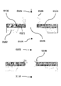
[0070] Turning now to the figures, FIG. 1A shows an example schematic of a
sensor in profile
view consistent with various aspects of the present disclosure. The sensor can
be used for
detection of nucleic acids 0105. The sensor comprises an electrode 0101
embedded in a pore
0104 disposed on a substrate 0102, which can be made by photolithography. In
some cases, the
pore has a diameter of between about 100 and about 300 rim. The signal from
the electrode can
be read through a thin-film unity gain source follower (SF) amplifier
integrated in close proximity
to the sensor (not shown, see FIG. 7, FIG. 11 and FIG. 13 for examples). The
nucleic acid
molecules to be detected can be immobilized on the sensor such that by
applying the appropriate
bias on the bias electrodes 0103, the negatively charged nucleic acid can be
drawn into the pore
for sensing 0106. The bias electrodes can be Ag/AgCl, Pt or Au electrodes. In
some cases, the
membrane 0100 (e.g., about 100 to about 400 nm thick) provides the electrical
confinement to
generate the non-equilibrium transport condition necessary for de-screening of
the electrical
double layer (EDL). FIG. 1B shows additional drawings of the sensor of the
present disclosure.
The pore 0107 has an embedded electrode 0108 connected to an amplifier 0109.
The nucleic acid
molecules 0110 to be detected can be immobilized on the sensor such that by
applying the
appropriate bias on the bias electrodes 0111, the negatively charged nucleic
acid can be drawn
into the pore for sensing 0112.
[0071] The sensor of the present disclosure can be used to detect any analyte
such as nucleic
acids, proteins, carbohydrates, metabolites, cells, organic or inorganic
molecules, drugs, and/or
drug candidates. The analyte itself need not have a charge. For example, FIG.
2 shows an
example of using the sensor for a sandwich immunoassay. A probe antibody 0200
can be
immobilized on the surface of the membrane 0204, near the pore 0205 entrance.
The analyte
(target antigen) 0201 can bind to the probe antibody, which is also bound to
the secondary
antibody 0202. The secondary antibody 202 can include an antibody conjugated
with a charged
CA 02951945 2016-12-09
WO 2015/196148 PCT/US2015/036800
21
tag that can be pulled into the pore 0203 for sensing when a trans-membrane
bias is applied by
the bias electrodes 0206. In some cases, the charged tag is a nucleic acid
molecule.
[0072] In another embodiment, FIG. 3 shows a chip architecture for analysis of
an analyte-
antibody interaction. The analyte molecule 0300 (e.g., a protein) is attached
to the membrane
0303 near the pore 0304. An antibody having a conjugated charged tag 0301 can
bind to the
analyte and be pulled into the pore 0302 for detection when a bias is applied
by the bias electrodes
0305.
[0073] The sensor can be packaged and integrated with electronic and/or
fluidic connections
(e.g., for operation in a device). FIG. 4 shows an example of a cross-
sectional schematic drawing
of a packaged chip. The packaged chip has a bottom fluidic cell 0400, a top
fluidic cell 0401, and
a middle fluidic cell 0402. A top external electrode 0403 and a bottom
external electrode 0404
can be attached to external electrode leads (0405 and 0406, respectively). The
sensor chip 0407
can be electrically addressed by a sensor chip input/output 0408.
[0074] The sensor can be an active sensor (i.e., having an integrated signal
amplifier) or a
passive sensor (i.e., not having an integrated signal amplifier). In some
cases, a passive sensor is
integrated with an external signal amplifier (i.e., an amplifier not
structurally embedded in the
pore sensor itself). In some instances, an active sensor consumes power and
requires a power
supply. The sensor of the present disclosure can be designed to have any
suitably high signal-to-
noise ratio (SNR) when operated as a passive or active sensor. In some
embodiments, the SNR
can be within a range of 1-100 (e.g., is about 1.1, about 1.2, about 1.5,
about 2, about 3, about 4,
about 5, about 6, about 7, about 8, about 9, about 10, about 15, about 20,
about 25, about 30,
about 40, about 50, about 100; at least about 1.1, at least about 1.2, at
least about 1.5, at least
about 2, at least about 3, at least about 4, at least about 5, at least about
6, at least about 7, at least
about 8, at least about 9, at least about 10, at least about 15, at least
about 20, at least about 25, at
least about 30, at least about 40, at least about 50, or at least about 100).
CA 02951945 2016-12-09
WO 2015/196148 PCT/US2015/036800
22
100751 FIG. 5A shows one strategy for enhancing the SIXTR of the sensor. The
sensor can have
a passive embedded sensing electrode 0500, a pore 0501, and charged analytes
immobilized in
proximity to the pore 0502. In some cases, there are a plurality of charged
analytes that are clonal,
but this is not required. A group of different charged analytes can be sensed
with a single pore,
however, without the ability to differentiate between the charged analytes, in
some
implementations. In some cases, there is only one pore in the sensor for each
colony of charged
analytes. However, the sensor of the present disclosure can have a plurality
of pores 0503 per
colony of charged analytes. Compared to a single pore, a plurality of pores
can enhance the SNR
by increasing the signal and/or decreasing the noise. In some embodiments,
there are 2, 3, 4, 5,
6, 7, 8, 9, 10, 12, 15, 20, 25, 30, 50, 100, 500 or 1000 pores per unique
charged analyte. In some
embodiments, there are at least 2, at least 3, at least 4, at least 5, at
least 6, at least 7, at least 8, at
least 9, at least 10, at least 12, at least 15, at least 20, at least 25, at
least 30, at least 50, at least
100, at least 500 or at least 1000 pores per unique charged analyte. In some
cases, the sensor
employs a plurality of pore/analyte repeats that are not necessarily arranged
in proximity to each
other on the sensor. However, the plurality of pores can also be arranged in
proximity to a colony
of the unique charged analyte and/or share a common sensing electrode 0500.
Having a plurality
of pores be addressed by a common sensing electrode can simplify the design of
the sensor and/or
facilitate miniaturization of the sensor array. FIG. 5B shows an embodiment of
the sensor of the
present disclosure having a plurality of pores 0504. The sensor has a top
insulator including
silicon dioxide (SiO2) 0505, a bottom insulator including silicon nitride
(Si3N4) 0506 and a
platinum (Pt) electrode 0507 disposed on a silicon (Si) substrate 0508. In
some embodiments, the
electrode has a thickness of about 75 nanometers (nm) (e.g., 70 nm Pt and 5 nm
titanium (Ti)),
the membrane has a thickness of 80 nm silicon nitride (Si3N4) and 70 nm SiO2.
The plurality of
pores can be defined by photolithography. The plurality of pores can be used
to enhance the net
charge delivered to the sensor (e.g., in absence of a dedicated integrated
amplifier).
CA 02951945 2016-12-09
WO 2015/196148 PCT/US2015/036800
23
[0076] In some embodiments, the sensor has an exposed electrode. As shown in
FIG. 6, the
exposed electrode 0600 can function as both the sensing electrode and as a
substrate onto which
the charged analyte 0601 can be immobilized.
[0077] FIG. 7A shows a profile drawing of two active sensors. The design
includes an
embedded sensing electrode 0700 for the active sensor, active transistors 0701
including the
dedicated amplifier, and interconnects 0702 for the active device. In another
embodiment, the
embedded sensing electrode 0703 can interface with a thin film transistor ( __
T) active amplifier
0704 and have interconnects 0705 for the active device. Both embodiments shown
here are
capable of detecting the charged analyte 0706.
[0078] FIG. 7B shows additional details of an active sensor of the present
disclosure having
enclosed top and bottom fluidic channels and their respective electrode
integrated into the device.
The sense electrode is sandwiched in the membrane with an integrated amplifier
in close
proximity. Such an architecture can reduce the noise arising from the sense
electrode. The rest of
the input/output (I/0) circuit can be located on a silicon wafer. The sensor
can have an integrated
top electrode 0707, a top fluidic cavity 0708, an integrated sensing amplifier
0709 as described
in FIG. 7A, a bottom fluidic cavity 0710, a bottom electrode 0711 and
peripheral circuitry 0712
on the substrate. In some cases, the substrate is silicon. As used generally
herein, any reference
to "top" or "bottom" are illustrative only, as the sensor can be oriented in
any way with respect to
gravity.
[0079] FIGs. 7C-7E show additional embodiments of an active sensor of the
present disclosure.
FIG. 7C has the amplifier away from the sense electrode in the silicon
substrate, which can
reduce the noise arising from the amplifier. This embodiment includes a top
fluidic channel 0713,
an analyte 0714, a sense electrode 0715, a pore sense area 0716, a bottom
fluidic channel 0717,
a cell amplifier 0718, a top fluidic electrode 0719, a bottom fluidic
electrode 0720, an I/O circuit
0721, an insulator 0722 and silicon 0723.
CA 02951945 2016-12-09
WO 2015/196148 PCT/US2015/036800
24
[0080] FIG. 7D has an open top fluidic channel and an enclosed bottom fluidic
channel, which
can negate the need to perform a complex bonding process. All of the active
components are on
the main silicon substrate, which can allow for robust operation but can
require a larger chip area
to implement. This embodiment can include an insulator 0724, an I/O circuit
0725, a top fluidic
channel 0726, a cell amplifier 0727, an analyte 0728, a sense electrode 0729,
a pore sensing area
0730, a bottom fluidic channel 0731, a bottom fluidic electrode 0732 and a
silicon substrate 0733.
[0081] FIG. 7E shows open top and bottom fluidic channels, which can enable
the use of
external channel electrodes. All of the active components are on the main
silicon substrate, which
can allow for robust operation but can require a larger chip area to
implement. This embodiment
can include an insulator 0734, an I/O circuit 0735, a top fluidic channel
0736, a cell amplifier
0737, an analyte 0738, a sense electrode 0739, a pore sensing area 0740, a
bottom fluidic channel
0741 and a silicon substrate 0742.
[0082] The sensor can be used to perform a number of analyses or measurements
generally
known in the art. hi some cases, the sensor of the present disclosure enables
improved methods
or performance thereof compared with the current state of the art. For
example, described herein
is a hybridization assay (i.e., microarray) that can be used to detect single
nucleotide
polymorphisms (SNPs). As shown in FIG. 8, the sensor has a charge sensing pore
0800 with an
integrated charge sensing electrode 0801 in proximity to immobilized
hybridization probes 0802.
In some cases, the hybridization probes are nucleic acid molecules that
hybridize with an analyte
0803. The analyte can be a second nucleic acid molecule having a sequence that
is complimentary
to the hybridization probe. Application of a bias across the pore can pull the
hybridization probes
and analytes (probe-analyte conjugate) into the pore for detection 0804
according to the methods
described herein. In some cases, a device of the present disclosure includes
an array of sensors,
each having a pore with a unique hybridization probe attached in proximity to
the pore. Each
pore-sensor pair can therefore detect a different analyte. However, in some
cases, the
hybridization probes immobilized near any given pore are not necessarily the
same (i.e., clonal).
25
A given pore can have 2, 3, 4, 5, 6, 7, 8, 9, 10, or more different types of
hybridization probes
associated with it. In some cases, each of the different hybridization probes
has a different analyte
that binds to it, with each analyte having a different charge. In this way, a
given pore can detect
and/or distinguish between 2, 3, 4, 5, 6, 7, 8, 9, 10, or more different
analytes.
[0083] The sensors described herein can be used to determine the sequence of
an analyte (e.g., a
nucleic acid molecule). FIG. 9A and FIG. 9B depict the operations that can be
used to perform
sequencing by synthesis (SBS), with the operations of FIG. 9B following those
of FIG. 9A in an
iterative fashion. As shown, the method uses a charge sensing pore 0900 and a
charge sensing
electrode 0901. A nucleic acid to be sequenced 0902 is immobilized in
proximity to the pore, for
example to adaptors coated on the perimeter of the pore suitable for solid-
phase amplification, as
shown in FIG. 10. The nucleic acid can be one of a library of nucleic acids,
each attached to a
separate adaptor in proximity to a separate sensor. The nucleic acid molecule
can be amplified
using solid-phase polymerase chain reaction (PCR) to form a colony of clonal
nucleic acid
molecules, also attached to the sensor in proximity to the pore, for example,
as described in the
International Patent Application Number PCT/AU1992/000587. An oligonucleotide
primer 0903
can hybridize with the nucleic acids to be sequenced, followed by washing away
of non-hybridized
primers. Application of an electrical field can draw the nucleic acid-primer
complex into the pore
0904 for measurement of a reference charge (i.e., prior to sequencing). The
reference charge can
be stored. This high electrical field can both pull the immobilized nucleic
acid into the sensor and
help de-screen the EDL.
[0084] Continuing with FIG. 9B, SBS can be performed by extending the primer
0903 by
incorporation of a nucleotide 0905 that is complimentary to the nucleic acid
molecule to be
sequenced at the subsequent base position 0906 (i.e., guanine (G) with
cytosine (C) and adenine
(A) with thymine (T) or uracil (U)). Excess or non-incorporated nucleotides
can be washed away
and/or degraded (e.g., with apyrase). Incorporation of the nucleotide
increases the negative charge
Date Recue/Date Received 2022-09-30
CA 02951945 2016-12-09
WO 2015/196148 PCT/US2015/036800
26
on the nucleic acid - primer complex by one electron (relative to the
reference charge and/or
charge measured at the previous iteration), which can be sensed by applying a
voltage across the
pore suitable for pulling the nucleic acid-primer complexes into the pore
0907. The sensed charge
can be compared with the reference and/or previous charge (which is optionally
stored in the
sensor) to make a base call. The SBS procedure described herein can continue
by iteratively
challenging the system with each of the four bases A, G, C, T (or U in the
case of RNA) in
succession, in any order. Instances in which the system was challenged with a
base that is not
complimentary to the subsequent base position will not result in a change in
charge. In some
cases, the change in charge is attributable to the increased length of the
phosphate backbone of
the growing primer strand, with one negative charge per base position. Those
skilled in the art
will appreciate that the incorporation of a nucleotide can be performed with a
polymerase enzyme
in the presence of a suitable buffer, including magnesium and/or manganese
ions.
[0085] FIG. 9C shows another depiction of a method for SBS using the sensor of
the present
disclosure and is similar to the steps described with reference to FIG. 9A and
FIG. 98. As shown,
the method uses a charge sensing pore 0908. A nucleic acid to be sequenced
0909 is immobilized
in proximity to the pore, for example to adaptors coated 0910 on the perimeter
of the pore suitable
for solid-phase amplification. The nucleic acid can be one of a library of
nucleic acids, each
attached to a separate adaptor in proximity to a separate sensor. The nucleic
acid molecule can
be amplified using solid-phase polymerase chain reaction (PCR) to form a
colony of clonal
nucleic acid molecules 0911. An oligonucleotide primer 0912 can hybridize with
the nucleic acids
to be sequenced, followed by washing away of non-hybridized primers.
Application of an
electrical field can draw the nucleic acid-primer complex into the pore 0913
for measurement of
a reference charge (i.e., prior to sequencing). SBS can be performed by
extending the primer by
incorporation of a nucleotide 0914 that is complimentary to the nucleic acid
molecule to be
sequenced at the subsequent base position. Excess or non-incorporated
nucleotides can be washed
away and/or degraded (e.g., with apyrase). Incorporation of the nucleotide
increases the negative
CA 02951945 2016-12-09
WO 2015/196148 PCT/US2015/036800
27
charge on the nucleic acid-primer complex by one electron (relative to the
reference charge and/or
charge measured at the previous iteration), which can be sensed by applying a
voltage across the
pore suitable for pulling the nucleic acid-primer complexes into the pore
0915.
[0086] Densely populated immobilized DNA can be provided to a sensor and solid-
phase PCR
amplification or bridge amplification can be performed. A gas phase
silanization of the chip
surface can be performed with molecular vapor deposition of (3-aminopropy1)-
trirnethoxysilane
(APTMS). Using the crosslinker N-(p-maleimidophenyl)isocyanate (PMPI), a thiol-
modified
oligonucleotide that acts as the PCR primer can be attached to the chip
surface. There are a variety
of other crosslinkers that can be used.
[0087] FIG. 10 shows an example of a process of covalently attaching nucleic
acids to the
charge sensor surface, consistent with various aspects of the present
disclosure. A SiO2 surface
1000 including hydroxide moieties 1001 (and/or that is hydroxylated) can be
silanized (e.g., using
aminosilane 1002). Silanization can be performed in gas phase. A crosslinker
(e.g., PMPI 1003)
can be used to connect the amine group on the silane and the sulfhydryl group
of the 5' thiol-
modified primer 1004. The resulting product of the surface chemistry described
herein is shown
at 1005.
[0088] In practice, sensing chips were plasma cleaned, rehydrated and
functionalized with (3-
aminopropy1)-trimethoxysilane (APTMS) using a chemical vapor deposition
system. The amino-
functionalized surfaces were subsequently transformed into a thiol-reactive
moiety by exposure
to a 2.3 mM solution of N-(p-maleimidophenyl) isocyanate (PMPI) in anhydrous
toluene at 40 C
for 2 hours under an argon atmosphere. The surfaces were subsequently washed
with anhydrous
toluene and dried in a stream of argon followed by DNA immobilization using
thiolated
oligonucleotides. Prior to immobilization the thiolated oligos were reduced
using tris(2-
carboxyethyl)phosphine (TCEP) as a reducing agent and desalted using a spin
column (MWCC
3000). Thiolated oligos can be spotted directly onto sensing chips for 6 hours
at 10 uM
concentration in a 1 M NaC1 buffer solution under a controlled atmosphere,
followed by extensive
CA 02951945 2016-12-09
WO 2015/196148 PCT/US2015/036800
28
washing. The various surface modification steps were followed by x-ray
photoelectron
spectroscopy and the presence of the expected elements and peak shifts
confirmed the
transformation of the sensing surface. The bridge PCR amplification itself is
done by thermal
cycling the sensor chip in a standard PCR tube along with the appropriate
reagents and a 900 base
pair (bp) template previously prepared. The result of the attachment chemistry
is a chain of
covalent bonds securely immobilizing 900 bp DNA molecules to the chip surface.
The length of
the 900 bp template was selected since its length is a close match to the
fabricated pore length.
The solid-phase amplified DNA molecules are linearized by a restriction
enzyme. The dense
presence of immobilized nucleic acid from solid-phase amplification is
verified by fluorescence
microscopy with appropriately excited SYBR Gold nucleic acids dye. FIG, 10
shows microscopy
images of the charge sensor chip with and without the immobilized DNA
molecules.
[0089] In order to verify that the result of fluorescence response is from
successful bridge
amplification and not from nonspecific binding, several control experiments
were carried out. In
each experiment, a component in the surface chemistry (aminosilane,
crosslinker and thiolated
oligo) was omitted prior to thermal cycling that nominally would result in PCR
amplification.
FIG. 10 shows the result. The absence of any of the components resulted in a
low level of
fluorescence signifying that the solid-phase PCR amplification is only
successful when all of
three surface chemistry components are in place as shown in 1008. Slightly
elevated fluorescence
brightness in the case where aminosilane was deposited and thiolated
oligonucleotide primers
were incubated without the presence of the crosslinker is speculated to be low
levels of non-
specific adhesion of negatively charged oligos to the positively charged amine
group of the
silanes.
[0090] FIG. 10 shows an example of an optical microscopy study of solid-phase
PCR amplified
DNA on the sensor surface, consistent with various aspects of the present
disclosure. A bright
field microscopy image 1006 of a sensor with solid-phase PCR amplified DNA of
ca. 900 bases
(the light gray area is the SiNõ /Si02 membrane) is shown. The dark porous
area is the Pt sense
CA 02951945 2016-12-09
WO 2015/196148 PCT/US2015/036800
29
electrode with the pore array. The 1 gm pores are defined by photolithography.
Also shown is a
fluorescence microscopy image 1007 of the chip at the location shown in 1006.
SYBR Gold-
stained DNA fluorescence signifies an abundance of DNA molecules and
successful solid-phase
PCR amplification. A series of control experiments, where a component in the
surface chemistry
has been omitted to enhance fluorescent brightness of the chip with various
missing surface
chemistry is shown at 1008.
[0091] With nucleic acids immobilized, a passive or active sensor chip,
consistent with various
aspects of the present disclosure, can be operated in the following fashion:
i) a positive potential
can be applied to the cathode, ii) application of the potential can create an
electric field near the
pore in such a way that the immobilized analyte (e.g., nucleic acid) molecules
are drawn into the
pore and iii) the analyte molecules' presence in the pore under an external
electric field leaves an
electrical signal onto the (e.g., platinum) sense electrode whose potential
can be recorded for
analysis. With the analyte covalently immobilized on the top surface, the
sensor's ability to
distinguish charge can be tested by observing the signal difference between a
negative control
experiment where there is no surface chemistry done to the sensor chips, chips
with single-
stranded (SS) DNA attached with 900 electrons (e-) per molecule, and chips
with double-stranded
(DS) DNA attached with 1800e- per molecule of charge.
[0092] FIG. 11 shows an example of a demonstration of a charge sensor,
consistent with various
aspects of the present disclosure. The schematic of the charge sensor setup
includes a current
amplifier 1100 connected to a top electrode 1101, a unity gain voltage
amplifier 1102 off the
chip, a sensing electrode 1103 (75 nm platinum electrode), an insulating
membrane 1104, a
bottom electrode 1105, and immobilized (linearized) nucleic acid molecules
1106 on the SiO2
surface. When positive potential is applied to the cathode, the nucleic acid
molecules are pulled
into the pore, altering the potential of the sense electrode 1103. The
measurements can be done
in low concentration salt (e.g., 100 piA4 KCI) to enhance the electrical
detection. As shown in the
bottom most part of FIG. 11, the sensor potential (output of 1102), can be
measured in units of
CA 02951945 2016-12-09
WO 2015/196148 PCT/US2015/036800
volts (V) and monitored 1107 while the applied cathode potential is increased
and shown in units
of milli-volts (mV) 1108. Each curve represents a measurement with a different
sensor chip (i.e.,
solid lines, short dashed lines and long dashed lines). The upper-most group
of lines 1109
represents a negative control where there was no nucleic acid attached. The
intermediate group
of lines 1110 represents those chips that have had 900 bases of SS DNA
attached to them. The
lower-most group of lines 1111 represents those chips that have had 900 base
pairs of DS DNA
attached. While some chip-to-chip variation is observed, overall the sensor is
able to differentiate
the net charge difference between the three cases. With a 100 mV difference
observed between
Ca. 900 bases, we see a 110 gV/base.
[0093] FIG. 12A shows electron microscopy images of the device described in
FIG. 11, Bond
pads 1200 are shown with 2x redundancy. The microporous sensor pore area 1201
can be attached
by a signal wire 1202. The sensor area can be served by a single platinum
electrode. The
micrographs also show the silicon substrate 1203 and a Si02/SiN., membrane
1204. FIG. 12B
shows two examples of electron micrographs of the pore of the sensor of the
present disclosure,
including a top view 1205 (SiO2 side) and a bottom view 1206 (Si3N4 side). The
scale bars are 1
gm and the measured pore diameters are Ca. 1.15 gm.
[0094] FIG. 13 shows an example of a charge sensor and result of operation of
the charge
sensor. The sensor has an exposed gold sense electrode 1300 as described in
FIG. 6. The sensor
further includes a SiN,, membrane 1301, 450 bp of DS DNA immobilized at one
thiolated 5' end
1302, a top electrode 1303, a bottom electrode 1304, a pore (2 gm in diameter)
1305, and a unity
gain amplifier 1306 providing a sensor signal output 1307. The sensor
potential (at 1307) is
plotted on the vertical axis in units of volts (V) 1308 as a function of
applied bias 1309 in units
of milli-volts (mV) (applied at 1304). Application of a negative bias to the
bottom electrode 1304
results in the nucleic acid molecules being pulled out of the pore 1310, and
no meaningful
difference in sensor potential being measured when nucleic acids are attached
to the sensor
(smaller diamond markers) versus a control without nucleic acid molecules
(larger square
CA 02951945 2016-12-09
WO 2015/196148 PCT/US2015/036800
31
markers), as shown in the left-most section of the plot 1311. Application of a
positive bias to the
bottom electrode 1304 results in the molecules pulled into the pore 1312. No
difference is
observed at low positive bias, as shown in the middle section of the plot
1313. However, at high
positive bias, the sensor potential is significantly reduced relative to the
control, as shown in the
right-most section of the plot 1314. At high positive bias, the control case
where no DNA were
attached to the chip 1315 shows the sensor output which mirrors the result of
negative bias
application, resulting in a symmetrical operation. At high positive bias, the
instance where DNA
molecules were attached to the chip 1316 results in successful detection of
nucleic acids charge.
10095] To demonstrate the operating principle, a cylindrically symmetric model
system was
simulated where a fragment of 60 bp double-stranded (DS) DNA is located at the
center (the most
challenging detection scenario) of an aqueous nanopore, as schematically shown
in FIG. 14A.
The system includes a cathode 1409, a metal electrode 1410, a solid dielectric
1411, a virtual
ground 1412, an anode 1413, and a charged molecule 1414. The Poisson-Nernst-
Planck (PNP)
equations along with the Stokes equations were solved to model the ionic and
fluidic transport
across the pores using the general partial differential equation solver
Prophet, to solve the
nonlinear, coupled model equations. The PNP equations are
V = (ei,V q(C ¨ C _) = 0;
qV = (¨ DV C ¨ p+C +V + C +0= 0; (Eq. 2),
¨ q V = (¨ D _V C _ + iu _C _V lit + C _fi)=
where a is the dielectric constant of the solution, q the elementary charge,
Di-and pi the diffusion
coefficients and mobilities of cations and anions, respectively. The fluid
transport is modeled by
the Stokes-divergence equations
¨ Vp + rAii ¨ (C+ C _)V = 0
V = = 0 (Eq. 3),
where p is the solvent pressure and y is the solvent viscosity. Table 1,
presented below, shows
values of important simulation parameters.
CA 02951945 2016-12-09
WO 2015/196148 PCT/US2015/036800
32
Table 1: Simulation Parameters and Values
Parameter Value
Solution dielectric constant (s,) 80 go
Insulator dielectric constant ( Ei ) 860
Cation/anion mobility ( p ) 7.62x 10⁻⁸ m2/Vs
Cation/anion diffusivity (D ) 2x10⁹ 1112/s
mM
Bulk ion concentration ('¨a)
Solvent viscosity ( 0.001 Ns/m2
DNA mobility ( p ) 3.5x10⁻⁸ m2/Vs
DNA diffusivity (D) 1.8x10⁻¹¹ m2/s
DNA source-end bulk concentration 2,7 nM
Example simulation results are presented in FIGs. 14B-D. The validity of the
simulator has been
shown by its ability to accurately simulate DNA translocation behavior through
gated pores of
similar dimensions for actuation application.
[0096] FIG. 14B shows example contour plots of simulated electrostatic
potential change due
to the presence of the charged molecule with 0 V and 7 V external electrical
biases applied,
consistent with various aspects of the present disclosure. At zero external
electrical bias 1400,
the Debye-Htickel screening behavior is observed. In contrast, for an
electrical bias of 7 V applied
across the pore 1401, significant long-range electrostatic interaction is
observed (as indicated by
lighter color and field lines). The membrane is modeled as a solid dielectric
layer of 500 nrn
thickness. The ionic solution is 1 mM 1(C1. The pore radius is set to 300 nm,
corresponding to
about 30 Debye lengths at this molar concentration.
[0097] Further simulations were performed with the device structure of FIG.
14A, which is
consistent with various aspects of the present disclosure. The sensing
efficiency, or the fraction
of induced charge, /3, has been calculated for different pore radii (as shown
in FIG. 14C) and
biasing conditions such as effective gate oxide thickness (a dielectric
insulator) (as shown in FIG.
14D).
CA 02951945 2016-12-09
WO 2015/196148 PCT/US2015/036800
33
[0098] With reference to FIG. 14C, the fraction of charge in the sensing
electrode induced by
the biomolecule at 1V 1402, 2V 1403 and 3V 1404 is shown when no oxide is
between the
electrode and solution. An example plot of the effect of dielectric formation
on the sense electrode
on sensing efficiency is shown in FIG. 14D at OV 1405, 1V 1406, 2V 1407 and 3V
1408. The
schematic plot shows the effect of dielectric formation on the sense electrode
on sensing
efficiency. This models the sensing metal electrode sandwiched between two
insulating layers.
Assuming the biomolecule charge is ¨Q, the induced charge in the metal
electrode is Q'¨flQ,
which is essentially the amount of charge sensed by the amplifier circuitry.
One conclusion of
this modeling can be that, with modest DC electrical bias across the pore, the
charge that can be
sensed is between about 20% and about 40% of the biomolecule charge for a 500
nm pore when
the biomolecule is at the center of the pore. In practice, the charge can be
delivered much closer
to the sense electrode due to the way in which the analyte (e.g., DNA) is
immobilized near the
periphery of the pore, rather than at the center.
[0099] FIG. 15 shows a circuit diagram for an individual sensor of the present
disclosure. The
sensor includes a sensing electrode 1500, which for convenience in making a
transistor analogy
can be referred to as a "gate". The sensor also has a top insulator 1501, a
top (or source) electrode
1504, a bottom insulator 1507, a bottom (or drain) electrode 1509, and a
channel position 1506
at which the sensing is modeled to occur. The top insulator 1501 and bottom
insulator 1507 can
be the same or optionally can be comprised of different materials. The circuit
model includes
various components including a capacitance CGS from the gate to the top
electrolyte body (or
source) 1502, a capacitance Cc from the gate to the channel 1503, a channel to
source resistance
RGs 1505, a channel to drain resistance RGD 1508, and a gate to drain
capacitance CGD 1510.
Equations are presented at 1511 and 1512 relating these elements with the
voltage at the source
(Vs), at the drain (VD), in the channel (Vc) and at the gate (VG).
[001001 FIG. 16 shows experimentally measured results corresponding to some of
the circuit
diagram elements described in FIG. 15, with the various graph lines
representing measurements
34
of various sensors. The impedance between the gate and drain 1600 is shown as
a function of
frequency. The declining slope of this plot 1601 represents CGD (at 1510), the
minimum of the plot
1602 represents RGD (at 1508), and the increasing slope of this plot 1603
represents the instrument's
inductance. The impedance between the gate and source 1604 is also shown as a
function of
frequency. The declining slope of this plot 1605 represents CGS (at 1502), the
minimum of the plot
1606 represents RGs(at 1505), and the increasing slope of this plot 1607
represents the instrument's
inductance.
[00101] The pore can be any suitable size or shape. The pore can be circular,
an oval, square,
rectangular, triangular, an elongated slit, or a polygon of 5, 6, 7, 8, 9, 10,
or more sides. The sensors
and methods of the disclosure can use a "nanopore", but do not require that
the pore be a nanopore,
which is generally defined to be a pore having a diameter at least about 1
nanometer (nm) and at
most about 5 nm or 10 nm. Without being held to any particular theory, this is
because the present
methods do not rely on blockage of ion flow through the pore by the analyte
being sensed, such as
described in U.S. Patent 6,428,959. Thus, the pore can be larger than a
nanopore, which enables a
more easily manufacturable and operable device. The pore of the present
disclosure can be made
from any suitable material (i.e., the pore can be a hole in the material),
including SiO2, SiN,
aluminum oxide (A1203), gold or mica. In some cases, the pore is a biological
pore, such as a protein
channel within a lipid membrane.
[00102] The side wall of the pore can have any suitable shape. In some
instances, the side wall is
straight and at a right angle to the surface of the membrane (e.g., as shown
in FIG. 1). In some
cases, the side wall is not at a right angle to the surface of the membrane.
The side wall can be
slanted. As shown in FIG. 17, the pore can be wider on the cis side (side of
the membrane where
the analyte is attached) than on the trans side of the membrane. The pore can
also be wider on the
trans side than on the cis side in some embodiments. In some cases, the pore
is hourglass shaped or
inverse hourglass shaped. The shape of the pore can be varied to manipulate
the properties of
Date Recue/Date Received 2022-09-30
CA 02951945 2016-12-09
WO 2015/196148 PCT/US2015/036800
the sense area 1700, for example in order to optimize any particular sensing
characteristic, such
as SNR. In some cases, a tapered pore geometry can result in more secure
and/or repeatable
placement of the analyte on the sensing electrode surface 1701.
[00103] FIG. 18 shows an example of the sensor chip interfacing with a printed
circuit board
(PCB). The PCB 1800 holds the sensor chip 1801 in a socket. Electrical
connections 1802, in this
instance, are made with wire bonding from the PCB to the sensor chip. The chip
and the wire
bond can be fluidically and electrically insulated with polydimethylsiloxane
(PDMS) 1803.
[00104] FIG. 19 shows an example of a fluidic cell that can be integrated with
the sensor. The
left portion of FIG. 19 depicts an exploded view drawing of the fluidic cells
to show inner
structure, while the right portion of FIG. 19 shows a photograph of the
fluidic cell when
assembled. The bottom fluidic cell 1900 can be made from
polytetrafluoroethylene (PTFE) and
can form a fluidic seal for the bottom fluidic reservoir 1901. The reservoir
can hold the electrolyte
and has an opening for the bottom electrode to make contact with the
electrolyte. The fluidic cell
can be designed to mount the sensor integrated with the PCB 1902 as described
in FIG. 18. The
top fluidic cell 1903 can also be made from PTFE and can form a fluidic seal
for the top fluidic
reservoir 1904. The top fluidic reservoir can hold electrolyte and have an
opening for the top
electrode to make contact with the electrolyte. The fluidic cell can also have
a reservoir for de-
ionized water 1905, which can help to humidify the environment in which the
device operates.
[00105] FIG. 20 shows an instrument capable of operating the sensor of the
present disclosure.
The instrument can be housed inside a faraday cage (e.g., made of solid
copper) 2000. The sensor
and fluidic cell described in FIG. 19 is shown 2001. The instrument can have
electrodes 2002,
an external amplifier circuit 2003, a battery 2004 for the amplifier circuit
and application of the
electrostatic potential and cables to control the instrument 2005.
[00106] FIG. 21A shows an example of an integrated sensor array. The array can
have any
number of sensors one skilled in the art would recognize, for example, the
particular number of
sensors is not important, whether the plurality of sensors is minimal or as
several/many million.
CA 02951945 2016-12-09
WO 2015/196148 PCT/US2015/036800
36
In some cases, each of the individual sensors of the array is individually
addressable. An
individually addressable sensor can be individually controlled (e.g., have a
bias applied to the
anode or cathode) and/or individually read (e.g., a signal derived from the
sensing electrode). In
some cases, a plurality of sensors of the array are addressable as a group. In
some instances, a
plurality of sensors share a common anode and/or cathode for applying an
electrical field across
the sensor.
[00107] Returning to FIG. 21A, the sensors can be addressed in any suitable
way and/or have
any suitable integrated circuitry. For example, each single cell of the charge
sensor 2100 can be
addressed by a vertical access circuit 2101. The array can also have a noise
reduction circuit 2102,
an analog-to-digital circuit 2103, and a horizontal access circuit 2104.
Details within a cell 2100
are shown, including power (e.g., VDD pin) 2105, a source follower amplifier
2106, a select 2107,
and data 2108. An example noise reduction circuit 2102 can include a reference
select 2109,
reference storage 2110, a comparator 2111, analog data out 2112, read storage
2113, and read
select 2114.
[00108] FIG. 21B and FIG. 21C show additional embodiments of sensor circuitry
for an
integrated sensor array of the present disclosure.
[0010911 FIG. 22 illustrates the physics of de-screening. When the system is
at equilibrium 2201,
the electrostatic potential ('l') shows a dramatic change within the Debye
length 2202 with
counter-ions 2200 effectively shielding the charge (-Q, e.g., DNA). The salt
concentration has an
effect on the Debye length according to the Debye-Htickel model. For example,
the Debye length
is about 1 nanometer (nm) for 100 millimolar (mM) potassium chloride (KC1),
about 3.4 nm for
mM KCl and about 10 run for 1 mM KC1. In contrast, at equilibrium, the net
counter-ion
current 2203 (Jnet) is approximately zero, where the drift component
(Coulombic attraction) of
counter-ion current (Jdriti) 2204 effectively balances the diffusion component
(Jdiff) 2205,
However, in the presence of an external field (non-equilibrium conditions),
the counter-ions can
CA 02951945 2016-12-09
WO 2015/196148 PCT/US2015/036800
37
flow 2206. The electrostatic potential is in non-equilibrium 2207, where the
net counter-ion
current is non-zero 2208 (i.e., positive) and the counter-ions flow.
1001101 The sensor of the present disclosure can be manufactured using any
technique, or
combination of techniques, such as photolithography. Table 2, presented below,
shows an
example of a method for making a passive sensor of the present disclosure.
Table 2 - Example Process for Manufacture of a Passive Sensor
Step Step description Note
0.0 Photo Alignment Mark
0.1 RCA1 and RCA2 clean
0.2 HMDS Prime
0.3 Resist Coat 1pm 3612 resist
0.4 Expose Alignment Marks ASML 80mJ/cm2
0.5 Develop
1 1.0 LPCVD Nitride
1.1 Diffusion Clean
1.2 LPCVD Stressed Nitride 50nm
2 2.0 Back Window Photo
2.1 RCA1 and RCA2 clean
2.2 HMDS Prime
2.3 Resist Coat 1pm 3612 resist
2.4 Expose Alignment Marks ASML 80mJ/cm2
2.5 Develop
2.6 Nitride RIE to expose bare Si
3 3.0 Photo Metal LO
3.1 RCA1 Resist strip
3.2 HMDS Prime
3.3 LOL 2000 Deposition 2k rpm 60s
3.4 Oven bake 190 C 10min
3.5 Resist Coat 1.6pm 3612 resist
3.6 Expose Metal ASML 120mJ/cm2
3.7 Develop
4 4.0 Metal Deposition & LO
4.1 lmin Ar Sputter clean of surface
4.2 Sputter deposition of 60nm Pt
4.3 Lift Off in Acetone overnight
5.0 Oxide Deposition
5.1 PECVD Oxide Deposition 30nm
5.2 ALD Oxide Deposition 20nm
6 6.0 Photo Contacts
6.1 PRS1000 Clean
6.2 HMDS Prime
6.3 LOL 2000 Deposition 2k rpm 60s
6.4 Oven bake 190 C lOrnin
CA 02951945 2016-12-09
WO 2015/196148 PCT/US2015/036800
38
Step Step description Note
6.5 Resist Coat 1.6pm 3612 resist
6.6 Expose Pads ASML 120mJ/cm2
7 7.0 Deposit Au and LO
7.1 1min Ar Sputter clean of surface
7.2 10nm Sputter Dep of Ti
7.3 200nm Sputter Dep of Au
7.4 Lift Off in Acetone overnight
8 8.0 Pore Photo
8.1 PRS1000 Clean
8.2 HMDS Prime
8.3 LOL 2000 Deposition 2k rpm 60s
8.4 Oven bake 190 C 10min
8.5 Resist Coat (Vary thickness for pore size) 1.6pm 3612
resist
8.6 Expose 1pm pores ASML 120mJ/cm2
8.7 Develop
8.8 Harden Resist 24hr5 110 C
9.0 Pore etch
9.1 Oxide RIE
9.2 Ar Sputter etch of Pt
9.3 Nitride RIE
10,0 Front surface protection
10.1 PRS1000 Clean
10.2 Protek3 Primer Deposition 1500rpm 60s
10.3 Oven bake 120 C 120s
10.4 Protek3 Deposition 1000rpm 60s
10.5 Oven bake 200 C 30min
11 - 11.0 Through wafer etch
11.1 TMAH etch 8% TMAH
12 12.0 Dice chips and clean
12.1 Wafer Saw dice chips
12.2 Remove Protek Step1 ACT-XT1100 27 C 30min
12,3 Remove Protek Step2 ACT 412 80 C 30min
12.4 PRS1000 Clean
13 13.0 Passivation
13.1 ALD Oxide Deposition 2.5nm
[001111 As illustrated, various modules and/or other circuit-based building
blocks may be
implemented to carry out one or more of the operations and activities
described herein and/or
shown in the Figures. In such contexts, these modules and/or building blocks
represent circuits
that carry out one or more of these or related operations/activities. For
example, in some
embodiments, one or more modules and/blocks are discrete logic circuits or
programmable logic
circuits configured and arranged for implementing these operations/activities,
as in the circuit
CA 02951945 2016-12-09
WO 2015/196148 PCT/US2015/036800
39
modules/blocks shown herein. In some cases, the programmable circuit is one or
more computer
circuits programmed to execute a set (or sets) of instructions (and/or
configuration data). The
instructions (and/or configuration data) can be in the form of firmware or
software stored in and
accessible from a memory (circuit). As an example, first and second
modules/blocks include a
combination of a CPU hardware-based circuit and a set of instructions in the
form of firmware,
where the first module/block includes a first CPU hardware circuit with one
set of instructions,
and the second module/block includes a second CPU hardware circuit with
another set of
instructions.
[00112] The present disclosure provides computer control systems that can be
employed to
regulate or otherwise control the sensors and methods provided herein. A
control system of the
present disclosure can be programmed to control process parameters to, for
example, sense an
analyte.
[00113] FIG. 23 shows a computer system 2301 that is programmed or otherwise
configured to
regulate the operation of the sensor. The computer system 2301 can regulate,
for example, flow
rates, temperatures, pressures, mechanical manipulations, applied voltages or
other electrical
inputs and/or outputs, and the like.
[00114] The computer system 2301 includes a central processing unit (CPU, also
"processor" and
"computer processor" herein) 2305, which can be a single core or multi core
processor, or a
plurality of processors for parallel processing. The computer system 2301 also
includes memory
or memory location 2310 (e.g., random-access memory, read-only memory, flash
memory),
electronic storage unit 2315 (e.g., hard disk), communication interface 2320
(e.g., network
adapter) for communicating with one or more other systems, and peripheral
devices 2325, such
as cache, other memory, data storage and/or electronic display adapters. The
memory 2310,
storage unit 2315, interface 2320 and peripheral devices 2325 are in
communication with the
CPU 2305 through a communication bus, such as a motherboard. The storage unit
2315 can be a
data storage unit (or data repository) for storing data.
CA 02951945 2016-12-09
WO 2015/196148 PCT/US2015/036800
[00115] The CPU 2305 can execute a sequence of machine-readable instructions,
which can be
embodied in a program or software. The instructions may be stored in a memory
location, such
as the memory 2310. Examples of operations performed by the CPU 2305 can
include fetch,
decode, execute, and writeback,
[00116] The storage unit 2315 can store files, such as drivers, libraries and
saved programs. The
storage unit 2315 can store programs generated by users and recorded sessions,
as well as
output(s) associated with the programs. The storage unit 2315 can store user
data, e.g., user
preferences and user programs. The computer system 2301 in some cases can
include one or more
additional data storage units that are external to the computer system 2301,
such as located on a
remote server that is in communication with the computer system 2301 through
an intranet or the
Internet.
[00117] The computer system 2301 can be in communication with a system 2330,
including a
device with integrated fluidics and/or process elements. Such process elements
can include
sensors, flow regulators (e.g., valves), and pumping systems that are
configured to direct a fluid.
[00118] Methods as described herein can be implemented by way of machine
(e.g., computer
processor) executable code stored on an electronic storage location of the
computer system 2301,
such as, on the memory 2310 or electronic storage unit 2315. The machine
executable or machine
readable code can be provided in the form of software. During use, the code
can be executed by
the processor 2305. In some cases, the code can be retrieved from the storage
unit 2315 and
stored on the memory 2310 for ready access by the processor 2305. In some
situations, the
electronic storage unit 2315 can be precluded, and machine-executable
instructions are stored on
memory 2310.
[00119] The code can be pre-compiled and configured for use with a machine
having a processer
adapted to execute the code, or can be compiled during runtime. The code can
be supplied in a
programming language that can be selected to enable the code to execute in a
pre-compiled or as-
compiled fashion.
CA 02951945 2016-12-09
WO 2015/196148 PCT/US2015/036800
41
1001201 Aspects of the systems and methods provided herein, such as the
computer system 2301,
can be embodied in programming. Various aspects of the technology may be
thought of as
"products" or "articles of manufacture" typically in the form of machine (or
processor) executable
code and/or associated data that is carried on or embodied in a type of
machine readable medium.
Machine-executable code can be stored on an electronic storage unit, such
memory (e.g., read-
only memory, random-access memory, flash memory) or a hard disk. "Storage"
type media can
include any or all of the tangible memory of the computers, processors or the
like, or associated
modules thereof, such as various semiconductor (circuit) memories, tape
drives, disk drives and
the like, which may provide non-transitory storage at any time for the
software programming. All
or portions of the software may at times be communicated through the Internet
or various other
telecommunication networks. Such communications, for example, may enable
loading of the
software from one computer or processor into another, for example, from a
management server
or host computer into the computer platform of an application server. Thus,
another type of media
that may bear the software elements includes optical, electrical and
electromagnetic waves, such
as used across physical interfaces between local devices, through wired and
optical landline
networks and over various air-links. The physical elements that carry such
waves, such as wired
or wireless links, optical links or the like, also may be considered as media
bearing the
software. As used herein, unless restricted to non-transitory, tangible
"storage" media, terms such
as computer or machine "readable medium" refer to any medium that participates
in providing
instructions to a processor for execution.
[001211 Hence, a machine readable medium, such as computer-executable code,
may take many
forms, including but not limited to, a tangible storage medium, a carrier wave
medium or physical
transmission medium. Non-volatile storage media include, for example, optical
or magnetic
disks, such as any of the storage devices in any computer(s) or the like, may
be used to implement
the databases, etc. shown in the drawings. Volatile storage media include
dynamic memory, such
as main memory of such a computer platform. Tangible transmission media
include coaxial
CA 02951945 2016-12-09
WO 2015/196148 PCT/US2015/036800
42
cables; copper wire and fiber optics, including the wires that comprise a bus
within a computer
system. Carrier-wave transmission media may take the form of electric or
electromagnetic
signals, or acoustic or light waves such as those generated during radio
frequency (RF) and
infrared OR) data communications. Common forms of computer-readable media
therefore
include for example: a floppy disk, a flexible disk, hard disk, magnetic tape,
any other magnetic
medium, a CD-ROM, DVD or DVD-ROM, any other optical medium, punch cards paper
tape,
any other physical storage medium with patterns of holes, a RAM, a ROM, a PROM
and EPROM,
a FLASH-EPROM, any other memory chip or cartridge, a carrier wave transporting
data or
instructions, cables or links transporting such a carrier wave, or any other
medium from which a
computer may read programming code and/or data. Many of these forms of
computer readable
media may be involved in carrying one or more sequences of one or more
instructions to a
processor for execution.
[00122] It should be understood from the foregoing that, while particular
implementations have
been illustrated and described, various modifications can be made thereto and
are contemplated
herein. For example, the embodiments described herein can be combined with or
modified to
yield yet more embodiments of the present invention. It is also not intended
that the invention be
limited by the specific examples provided within the specification. While the
invention has been
described with reference to the aforementioned specification, the descriptions
and illustrations of
the preferable embodiments herein are not meant to be construed in a limiting
sense. Furthermore,
it shall be understood that all aspects of the invention are not limited to
the specific depictions,
configurations or relative proportions set forth herein which depend upon a
variety of conditions
and variables. Various modifications in form and detail of the embodiments of
the invention will
be apparent to a person skilled in the art. It is therefore contemplated that
the invention shall also
cover any such modifications, variations and equivalents. It is intended that
the following claims
define the scope of the invention and that methods and structures within the
scope of these claims
and their equivalents be covered thereby.