Note : Les descriptions sont présentées dans la langue officielle dans laquelle elles ont été soumises.
CA 02957664 2017-02-10
OPTICAL FILTER ARRAY
BACKGROUND
[0001] In an optical device, such as a sensor element array, sensor
elements may be
associated with a particular spacing. For example, a first sensor element may
be associated
with a particular spacing from a second sensor element. The sensor elements
may be
associated with a size of between approximately 50 micrometers (vim) and 200
pm. The
spacing between a pair of sensor elements may be greater than approximately 20
gm. A
sensor element array may be used for a sensing system, such as a three-
dimensional depth
sensing system or the like.
SUMMARY
[0002] According to some possible implementations, a device may include a
filter array
disposed on a substrate. The filter array may include a first mirror disposed
on the substrate.
The filter array may include a plurality of spacers disposed on the first
mirror. A first spacer,
of the plurality of spacers, may be associated with a first thickness. A
second spacer, of the
plurality of spacers, may be associated with a second thickness that is
different from the first
thickness. A first channel corresponding to the first spacer and a second
channel
corresponding to the second spacer may be associated with a separation width
of less than
approximately 10 micrometers (t.tm). The filter array may include a second
mirror disposed
on the plurality of spacers.
[0003] According to some possible implementations, a device may include a
filter array
disposed on a substrate. The filter array may include a first mirror disposed
on the substrate.
The filter array may include a spacer disposed on the first mirror. The spacer
may include a
plurality of spacer layers. A first spacer layer, of the plurality of spacer
layers, may be
1
CA 02957664 2017-02-10
disposed to cover the first mirror. A second spacer layer, of the plurality of
spacer layers,
may be disposed onto the first spacer layer. A first channel corresponding to
the first spacer
layer and a second channel corresponding to the second spacer layer may be
associated with a
separation width of less than approximately 5 micrometers (aull). The filter
array may
include a second mirror disposed on the spacer.
[0004] According to some possible implementations, a device may include a
filter array
disposed on a substrate. The substrate may be a glass substrate to be bonded
to a sensor
element array or a silicon substrate including the sensor element array. The
filter array may
include a first mirror disposed on the substrate. The filter array may include
a plurality of
spacer layers. A first spacer layer, of the plurality of spacer layers, may be
disposed onto the
first mirror and covering a set of sensor elements of the sensor element
array. A second
spacer layer, of the plurality of spacer layers, may be disposed onto the
first spacer layer and
covering a subset of the set of sensor elements. A third spacer layer, of the
plurality of spacer
layers, may be disposed onto the second spacer layer and covering a subset of
the subset of
sensor elements. Each sensor element, of the set of sensor elements, may be
associated with
a spacing of less than approximately 1 micrometer ( ,m). The filter array may
include a
second mirror disposed on the plurality of spacer layers. The second mirror
may be aligned
with the set of sensor elements.
BRIEF DESCRIPTION OF THE DRAWINGS
[0005] Figs. lA and 1B are diagrams of an example of a dielectric based
optical filter
coating, as described herein;
[0006] Fig. 2 is a diagram of an example of an induced transmission filter
(ITF) based
optical filter coating, as described herein;
2
CA 02957664 2017-02-10
[0007] Fig. 3 is a diagram of an overview of an example implementation, as
described
herein;
[0008] Figs. 4A-4E are diagrams of an example implementation an optical
filter coating,
as described herein; and
[0009] Figs. 5A-5E are diagrams of an example implementation of an optical
filter
coating for a depth sensing system, as described herein.
DETAILED DESCRIPTION
[0010] The following detailed description of example implementations refers
to the
accompanying drawings. The same reference numbers in different drawings may
identify the
same or similar elements.
[0011] In an optical device, such as a sensor element array, sensor
elements may be
spaced by a particular distance. The sensor elements may be associated with a
size of
between approximately 50 micrometers (rim) and 200 j.tm. Spacing between a
pair of sensor
elements may be greater than approximately 20 p.m. However, as quantities of
sensor
elements included in a single optical device increase and/or as package sizes
for optical
devices decrease, it may be advantageous to manufacture sensor element arrays
of sensor
elements with a spacing of less than approximately 20 pm, less than
approximately 10 1.tm,
less than approximately 1 kim, or the like. Implementations, described herein,
may provide
an optical filter to enable a sensor element array of sensor elements with a
spacing of less
than a threshold value, such as less than approximately 20 um, less than
approximately 10
ptm, less than approximately 1 [tm, or the like.
[0012] Figs. lA and 1B are diagrams of an example 100 of a dielectric based
optical filter
coating, as described herein. As shown in Fig. 1A, example 100 includes a
substrate 110, a
photodiode 120, a photoresist layer 130, a filter coating layer 140, and a
transition area 150.
3
CA 02957664 2017-02-10
[0013] With regard to Fig. 1A, the dielectric based optical filter coating
is manufactured
on substrate 110, which may be an active device wafer, using a lift-off
process. The lift-off
process may be selected based on a difficulty in chemical etching, physical
etching, or the
like. Photoresist layer 130 is disposed onto regions of substrate 110 where
filter coating layer
140 is not to be deposited. For example, based on filter coating layer 140
being intended to
be deposited to cover photodiode 120 or another type of sensor element,
photoresist layer 130
is disposed on portions of substrate 110 that are not aligned to photodiode
120. After
deposition of filter coating layer 140 onto photoresist layer 130 and an
exposed portion of
substrate 110 that is aligned with photodiode 120, a lift-off process is
performed to remove
photoresist layer 130, resulting in filter coating layer 140 remaining at the
portion of substrate
110 aligned to photodiode 120. However, the lift-off process results in
transition area 150
where filter coating layer 140 is associated with a tapered edge of reducing
physical
thickness. Transition area 150 may be associated with a width of between
approximately two
and three times a thickness of filter coating layer 140.
[0014] As shown in Fig. 1B, in a top-view 160-1 and a side-view 160-2, a
set of
photodiodes 120-1 and 120-2 may be positioned in substrate 110, and may be
covered by a
set of filter coating layers 140-1 and 140-2 such that filter coating layer
140-1 overlaps with
filter coating layer 140-2. Overlapping filter coating layers 140 reduces a
spacing between
photodiode 120-1 and photodiode 120-2 relative to separating filter coating
layers 140. In
this case, filter coating layers 140 are associated with a thickness 172, a
photodiode area 174
(e.g., an area that is aligned with a corresponding photodiode 120, and a
functional area 176
(e.g., an area that is disposed between tapered edges of the particular filter
coating layer 140).
Photodiodes 120 may be associated with a separation width 178 (e.g., a spacing
between
photodiodes 120). Separation width 178 may be greater than three times
thickness 172. In
this case, thickness 172 is greater than approximately 5 micrometers (ptm)
resulting in
4
CA 02957664 2017-02-10
separation width 178 being great than approximately 15 pm. However, it may be
advantageous to achieve separation widths between photodiodes of less than 15
p.m, less than
p.m, less than 5 p.m, less than 1 pm, or the like.
[0015] As indicated above, Figs. lA and 1B are provided merely as an
example. Other
examples are possible and may differ from what was described with regard to
Figs. lA and
1B.
[0016] Fig. 2 is a diagram of an example 200 of an induced transmission
filter (ITF)
based optical filter coating, as described herein. As shown in Fig. 2, example
200 includes a
substrate 210, a photodiode 220, a photoresist layer 230, a filter coating
layer 240, which
includes a metal layer 240', and a transition area 250.
[0017] With regard to Fig. 2, metal layer 240' may include a silver (Ag)
layer, an
aluminum (Al) layer, or the like. Metal layer 240' may be encapsulated by a
dielectric
portion of filter coating layer 240 that reduces a likelihood of corrosion
relative to exposing
metal layer 240'. In this case, to manufacture filter coating layer 240 to
provide protective
encapsulation, the tapered edge of filter coating layer 240 is manufactured to
have less than a
threshold internal angle 260, such as less than approximately 5 degrees. The
ITF based
optical filter coating may be less than approximately 1000 nanometers (nm) in
thickness,
such as approximately 500 nm, but based on threshold internal angle 260 being
less than
approximately 5 degrees, transition area 250 may be approximately 10 m to 20
m, which
may correspond to a spacing between photodiodes 220 of between approximately
10 pm to
um. This may be larger than is advantageous for sensor element arrays that are
to include
sensor elements, such as photodiodes 220, that are sized between approximately
2 pm and 50
p.m and are to be associated with a spacing of between approximately 0.5 pm
and 10 m.
[0018] As indicated above, Fig. 2 is provided merely as an example. Other
examples are
possible and may differ from what was described with regard to Fig. 2.
5
= CA 02957664 2017-02-10
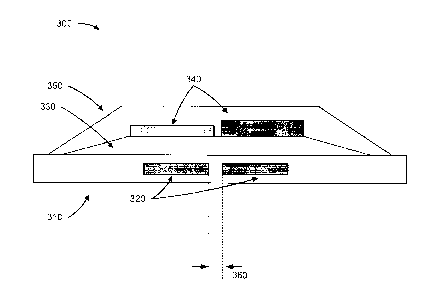
[0019] Fig. 3 is a diagram of an overview of an example implementation
300. Example
implementation 300 illustrates a single cavity Fabry-Perot filter based
optical filter coating,
as described herein, that is associated with a spacing of less than a
threshold value for sensor
elements of a sensor element array, such as a spacing of less than
approximately 10 um, less
than approximately 5 itm, less than approximately 1 um, or the like. As shown
in Fig. 3,
example implementation 300 includes a substrate 310, a set of photodiodes 320,
a first mirror
layer 330, a set of spacer layers 340, a second mirror layer 350. Photodiodes
320 are
associated with a spacing of separation width 360.
[0020] In some implementations, substrate 310 may be associated with a
wafer width of
between approximately 50 millimeters (mm) and 500 mm, such as an approximately
100 mm
width, an approximately 150 mm width, an approximately 200 mm width, an
approximately
300 mm width, an approximately 450 mm width, or the like. In some
implementations,
substrate 310 may be associated with a thickness of between approximately 50
tun and 1.0
mm. In some implementations, when substrate 310 is associated with a back-
illuminated
photodiode 320, substrate 310 may be associated with thickness of between
approximately 5
pm and 70 um, between approximately 25 um and 50 um, or the like, which may
be, for
example, temporarily bonded to a carrier wafer of another thickness.
[0021] In some implementations, photodiodes 320 may be associated with a
width of
between approximately 1 tun and 20 tun. In some implementations, a mirror,
such as first
mirror layer 330 or second mirror layer 350 may be associated with a thickness
of between
approximately 20 nanometers (nm) and 80 nm. In some implementations, spacer
layers 340
may be associated with a thickness of between approximately 15 nm and 300 nm.
[0022] With regard to Fig. 3, first mirror layer 330 and second mirror
layer 350 sandwich
a set of spacer layers 340. Spacer layers 340 may be deposited using a
physical vapor
deposition procedure, a chemical vapor deposition procedure, or the like to
vary thicknesses
6
CA 02957664 2017-02-10
of the set of spacer layers 340 and channels formed thereby. Based on varying
thicknesses of
the set of spacer layers 340, each photodiode 320, or another type of sensor
element, is
exposed to corresponding varying center wavelengths of light. In this way, an
optical filter
coating may be manufactured that permits separation width 360 to be less than
a threshold
value, such as less than 10 vtm, less than 5 m, less than 1 m, less than 500
nm, or the like.
In some implementations, separation width 360 may be between approximately 0.5
i_tm and
tim. In some implementations, separation width 360 may be approximately 150
nm.
[0023] As indicated above, Fig. 3 is provided merely as an example. Other
examples are
possible and may differ from what was described with regard to Fig. 3.
[0024] Figs. 4A-4E are diagrams of example implementations 400/400'/400" of
a single
cavity Fabry-Perot filter based optical filter coating, as described herein.
As shown in Fig.
4A, example implementation 400 includes a substrate 410, a set of photodiodes
420-1 to 420-
4, a first mirror layer 430, a set of spacer layers 440-1 to 440-4, and a
second mirror layer
450.
[0025] With regard to Fig. 4A, first mirror layer 430 and second mirror
layer 450 may be
quarterwave stacks using layers of silicon dioxide (Si02) and hydrogenated
silicon (Si:H or
Si_H). In another example, the quarterwave stacks may utilize another set of
materials, such
as another high refractive index material (e.g., niobium pentoxide (Nb205),
tantalum
pentoxide (Ta205), titanium dioxide (Ti02), hafnium dioxide (Hf02), a
combination thereof,
or the like), another low refractive index material (e.g., magnesium fluoride
(MgF2) or the
like), or the like. In some implementations, a non-fluoride based material may
be preferred to
reduce a difficulty of deposition. In some implementations, a material with
associated with a
relatively higher effective index may be preferred to reduce an angle-shift,
to reduce a
quantity of layers of a blocker or mirror, or the like. Spacer layers 440 may
be spacers
manufactured using one or more layers of hydrogenated silicon. In another
example, spacer
7
CA 02957664 2017-02-10
layers 440 may include another material, such as Nb205, Ta205, Ti02, Hf02,
another type
of oxide, a combination thereof, or the like. First mirror layer 430 and/or
second mirror layer
450 may be disposed in alignment with sensor elements, such as photodiodes
420.
[0026] In another example, semi-transparent metal mirrors may be used
rather than
quarterwave stacks, as described herein. For example, a metal mirror including
a silver (Ag)
layer may be used for an ultraviolet (UV)-A spectral range, a visible spectral
range, a near
infrared spectral range (NIR), or the like. Similarly, a metal mirror
including an aluminum
(Al) layer may be used for a UV spectral range or the like (approximately 200
nm to 400 nm
range).
[0027] In some implementations, first mirror layer 430 may include a
blocker layer
disposed on a surface of first mirror layer 430, a protective layer disposed
on a surface of first
mirror layer 430, or the like. Each spacer layer 440 is associated with a
particular thickness
that corresponds to a particular center wavelength of light being passed to a
corresponding
photodiode 420 or another type of sensor element. For example, as shown in
table 460,
spacer layer 440-1 may be associated with a thickness of approximately 96.6
nm, spacer layer
440-2 may be associated with a thickness of approximately 115.3 nm, spacer
layer 440-3 may
be associated with a thickness of approximately 131.5 nm, and spacer layer 440-
4 may be
associated with a thickness of approximately 147.6 nm. In this case, each
spacer layer 440
may be deposited onto first mirror layer 430 using a set of patterning and
coating steps for
each spacer layer 440. As shown, second mirror layer 450 may be deposited onto
exposed
portions of first mirror layer 430 and spacer layers 440, thereby
encapsulating spacer layers
440 with first mirror layer 430. In this way, a spacing between photodiodes
220 or other
sensor elements of between approximately 600 nm and 10 um, less than
approximately 600
nm, or the like may be achieved.
8
CA 02957664 2017-02-10
[0028] In some implementations, spacer layers 440 may be deposited using a
physical
vapor deposition (PVD) procedure. For example, spacer layers 440 and/or other
portions of
implementations described herein may be manufactured using a magnetron
sputtering
procedure, an e-beam and thermal evaporation procedure, and/or the like. In
some
implementations, spacer layers 440 may be deposited using a chemical vapor
deposition
(CVD) procedure. In some implementations, a thickness of spacer layers 440 may
be
selected to achieve a particular spectral range of light, such as a UV
spectral range (e.g.,
approximately 200 nm to 400 nm), a visible spectral range (e.g., approximately
400 nm to
700 nm), an NIR spectral range (e.g., approximately 700 nm to 2000 nm), a mid-
wavelength
IR (MWIR) spectral range (e.g., approximately 2 um to 6 um), a low-wavelength
IR (LWIR)
spectral range (e.g., approximately 6 um to 14 um), or the like. The
thicknesses of layers
may be related to a desired spectral range. For example, for a spectral range
of
approximately 2 um to 6 um or approximately 6 um to 14 um, thicknesses of
mirror layers
430 or 450 may be between approximately 20 nm and 400 nn, spacer layers 440
may be
between approximately 15 nm and 1500 nm, or the like. In some implementations,
spacer
layers 440 may be deposited to manufacture a silicon-based detector, an indium
gallium
arsenide (InGaAs)-based detector, or the like. In some implementations, spacer
layers 440
may be deposited for a hyperspectral imaging sensor. In some implementations,
spacer
layers 440 may be deposited for a back-illuminated sensor or a front-
illuminated sensor.
[00291 As shown in Fig. 4B, a similar example implementation 400' includes
a substrate
410, a set of photodiodes 420-1 to 420-4, a first minor layer 430, a set of
spacer layers 440-1
to 440-4, and a second mirror layer 450.
[0030] With regard to Fig. 4B, spacer layer 440-1 is deposited to cover all
of first mirror
layer 430 and each photodiode 420, and each other spacer layer 440 is
deposited onto spacer
layer 440-1. In this way, example implementation 400' is associated with a
reduced quantity
9
CA 02957664 2017-02-10
of patterning and coating steps that are to be performed to deposit spacer
layers 440 relative
to the patterning and coating steps that are performed to deposit spacer
layers 440 of example
implementation 400. In some implementations, when a mirror layer, such as
mirror layer
430, is a metal mirror layer (e.g., a silver based material), a spacer layer,
such as spacer layer
440-1, may provide a protective coating of the metal mirror layer. In another
example, each
of spacer layers 440-2 to 440-4 may be patterned and coated onto first mirror
layer 430, and
spacer layer 440-1 may be deposited onto exposed portions of first mirror
layer 430 and each
of spacer layers 440-2 to 440-4 before depositing second mirror layer 450. In
other words, an
entire surface of first spacer layer 440-1 is disposed contiguous to the
surface of second
mirror layer 450 rather than contiguous to first mirror layer 430. As shown in
table 460',
each of spacer layers 440-2 to 440-4 is associated with a particular thickness
in addition to
the thickness of spacer layer 440-1 (e.g., approximately 96.6 nm). For
example, spacer layer
440-2 is associated with an additional thickness of approximately 18.7 nm,
spacer layer 440-3
is associated with an additional thickness of approximately 34.9 nm, and
spacer layer 440-4 is
associated with an additional thickness of approximately 51 nm.
[0031] As shown in Fig. 4C, a similar example implementation 400" includes
a substrate
410, a set of photodiodes 420-1 to 420-4, a first mirror layer 430, a set of
spacer layers 440-1
to 440-4, and a second mirror layer 450.
[0032] With regard to Fig. 4C, spacer layer 440-1 is deposited onto first
mirror layer 430
and covers each of photodiodes 420-1 to 420-4. Similarly, spacer layer 440-2
is deposited
onto a portion of spacer layer 440-1 and covers each of photodiodes 420-2 to
420-4.
Similarly, spacer layer 440-3 is deposited onto a portion of spacer layer 440-
2 and covers a
subset of photodiodes 420 (e.g., each of photodiodes 420-3 to 420-4).
Similarly, spacer layer
440-4 is deposited onto a portion of spacer layer 440-3 and covers photodiode
420-4. In this
way, example implementation 400" reduces a quantity of patterning and coating
steps that
CA 02957664 2017-02-10
=
are to be performed to deposit spacer layers 440 in example implementation
400. As shown
in table 460", each of spacer layers 440-2 to 440-4 is associated with a
thickness in addition
to the thickness of a previous spacer layer 440. For example, spacer layer 440-
2 is associated
with an additional thickness of approximately 18.7 nm deposited onto spacer
layer 440-1
(e.g., which is associated with a thickness of approximately 96.6 nm), spacer
layer 440-3 is
associated with an additional thickness of approximately 16.2 nm deposited
onto spacer layer
440-2, and spacer layer 440-4 is associated with an additional thickness of
approximately
16.1 nm deposited onto spacer layer 440-3. In this way, a spacing between
photodiodes 220
or other sensor elements of between approximately 150 nm and 2 i_tm, less than
approximately 150 nm, or the like may be achieved.
[0033] As shown in Fig. 4D, a chart 470 identifies a set of optical
characteristics relating
to channels of example implementations 400/400'/400". For example, for a first
channel
associated with spacer layer 440-1 and photodiode 420-1, a thickness of spacer
layer 440-1
results in a center wavelength of approximately 795 nm. Similarly, for a
second channel
associated with spacer layer 440-2 and photodiode 420-2, a thickness of spacer
layer 440-2
results in a center wavelength of approximately 870 nm. Similarly, for a third
channel
associated with spacer layer 440-3 and photodiode 420-3, a thickness of spacer
layer 440-3
results in a center wavelength of approximately 935 nm. Similarly, for a
fourth channel
associated with spacer layer 440-4 and photodiode 420-4, a thickness of spacer
layer 440-4
results in a center wavelength of approximately 1000 nm. Although described
herein in
terms of a particular set of center wavelengths, other center wavelengths are
possible and
may differ from what was described with regard to Fig. 4D.
[0034] As shown in Fig. 4E, a chart 480 identifies a set of physical
characteristics relating
example implementations 400/400'/400". For example, a mirror, such as mirror
layer 430 or
mirror layer 450, may be associated with a thickness of between approximately
40 nm and
11
CA 02957664 2017-02-10
500 nm. Similarly, a spacer layer, such as spacer layer 440-4 may be
associated with a
thickness of approximately 147.61 nm. In some implementations, mirror layers,
such as
mirror layer 430 or mirror layer 450 may be associated with multiple layers.
For example,
mirror layers may include Si:H layers, Si02 layers, etc.
[0035] As indicated above, Figs. 4A-4E are provided merely as examples.
Other
examples are possible and may differ from what was described with regard to
Figs. 4A-4E.
[0036] Figs. 5A-5E are diagrams of an example implementation 500 of an
optical filter
coating for a depth sensing system, as described herein. As shown in Fig. 5A,
example
implementation 500 includes a substrate 510 (e.g., silicon nitride (S3N4) or
in another
example SiO2 or Si), a set of zinc oxide (ZnO) layers 520-1 to 520-4, a set of
silver (Ag)
layers 530-1 to 530-2, a set of niobium titanium oxide (NbTiOx) layers 540-1
to 540-3, and a
set of silicon dioxide (Si02) layers 550-1 to 550-2. In some implementations,
the optical
filter coating of example implementation 500 may be a Fabry-Perot optical
filter. In some
implementations, another example may include a transparent substrate 510 that
is bonded to a
sensor device.
[0037] With regard to Fig. 5A, ZnO layers 520 may be each associated with a
thickness
of approximately 1.5 nm. Ag layers 530, which are a set of semi-transparent
metal mirrors
encapsulating a set of spacer layers formed by NbTiOx 540-1, are associated
with a thickness
of approximately 40 nm. NbTiOx 540-1 may correspond to the spacers 440 in
Figs. 4A-4C,
resulting in differing thicknesses for NbTiOx 540-1 corresponding to a spacer
thickness that
is desired. As shown by table 560, NbTiOx 540-1 may form a set of three
channels for
visible light (e.g., red/green/blue (RGB) light) detection for image sensing
and a fourth
channel (e.g., IR and blue light) for depth sensing (e.g., three-dimensional
depth sensing).
Collectively, the four channels may correspond to spacers 440-1 through 440-4
shown in
Figs. 4A-4C. A first channel for blue visible light detection may be
associated with a total
12
CA 02957664 2017-02-10
thickness of approximately 44.8 nm, a second channel for green visible light
detection may
be associated with a total thickness of approximately 60.5 nm, a third channel
for red visible
light detection may be associated with a total thickness of approximately 82.9
nm, and the
fourth channel for IR and blue light detection (i.e., depth sensing) may be
associated with a
total thickness of approximately 134.5 nm. In some implementations, layers of
NbTiOx 540-
1 may be deposited in a form as shown in Figs. 4A-4C. For example, each
channel may be a
separate filter layer stack, each channel may share a common first filter
layer, each channel
may be deposited on a portion of a previously deposited filter layer, or the
like. In this case,
depositing at least one layer common to each channel, as in Figs. 4B and 4C,
may improve
durability of Ag layers 530 by providing a protective layer.
[0038] With further regard to Fig. 5A, NbTiOx layer 540-2 may be associated
with a
thickness of approximately 50 =, Si02 layer 550-1 may be associated with a
thickness of
approximately 18 nm, NbTiOx layer 540-3 may be associated with a thickness of
approximately 16 nm, and Si02 layer 550-2 may be associated with a thickness
of
approximately 101 nm. Layers 540-2, 550-1, 540-3, and 550-2 may collectively
form an
anti-reflection coating for sensor elements embedded in substrate 510 or
disposed onto
substrate 510.
[0039] As shown in Fig. 5B, a chart 570 identifies a set of optical
characteristics relating
to channels of example implementation 500. For example, the first channel
associated with
red visible light sensing is associated with a center wavelength of
approximately 620 nm.
Similarly, the second channel associated with green visible light sensing is
associated with a
center wavelength of approximately 520 =. Similarly, the third channel
associated with
blue visible light sensing is associated with a center wavelength of
approximately 450 nm.
Similarly, the fourth channel associated with depth sensing (e.g., blue light
and IR lights
sensing) is associated with center wavelengths of approximately 450 nm (blue
light) and 850
13
CA 02957664 2017-02-10
nm (IR light). Although described herein in terms of a particular set of
center wavelengths,
other center wavelengths are possible and may differ from what was described
with regard to
Fig. 5B.
[0040] As shown in Fig. 5C, a diagram 580 identifies a sensor element array
of sensor
elements relating to example implementation 500. For example, the sensor
element array
(e.g., a complimentary metal-oxide-semiconductor (CMOS) technology, a charge-
coupled
device (CCD) technology, or the like) includes a set of first channels (e.g.,
red light channels,
identified as R), a second of second channels (e.g., green light channels,
identified as G), a set
of third channels (e.g., blue light channels, identified as B), and a set of
fourth channels (e.g.,
IR and blue light channels, identified as IR/B). In this case, spacer layers
for the sensor
element array are manufactured by depositing each spacer layer on a portion of
the previous
spacer layer, as described herein with regard to Fig. 4C. This results in the
IR/B channels
having the greatest thickness, relative to other channels, of approximately
51.6 nm. Based on
that thickness, spacing of sensor elements of the sensor element array may be
approximately
150 nm.
[0041] In some implementations, the sensor elements may be back illuminated
sensor
elements to provide an improved quantum efficiency and spectral response
reproducibility
relative to another configuration of sensor elements. In some implementations,
a dielectric
blocker may be applied to the IR/B channels with a thickness of approximately
750 nm,
resulting in a spacing of approximately 2 um. Although described herein in
terms of a
particular pattern for arranging four spectral ranges of channels, other
patterns and/or other
quantities of channels may be possible. For example, although diagram 580
depicts a sensor
element array with 64 channels, implementations, described herein, may be used
with another
quantity of channels less than a threshold, such as less than or equal to 64
channels (e.g., 64
channels, 63 channels, 62 channels, ..., 2 channels, etc.), less than or equal
to 32 channels,
14
CA 02957664 2017-02-10
less than or equal to 16 channels, less than or equal to 8 channels, less than
or equal to 4
channels, or the like. In another example, another quantity of sensor elements
(i.e., pixels)
may be included. For example, implementations described herein may be utilized
for a pixel
count of between approximately 10 million pixels and 40 million pixels,
between
approximately 250 thousand pixels and 40 million pixels, or the like.
Additionally, or
alternatively, implementations described herein may be utilized for a pixel
count greater than
approximately 250 thousand, a pixel count greater than approximately 1
million, a pixel
count greater than approximately 4 million, a pixel count greater than
approximately 20
million, or the like.
[0042] With
regard to Fig. 5D, a diagram 590 and a diagram 590' are provided to identify
example optical characteristics relating to an angle shift of sensor elements.
Diagrams 590
and 590' show an angle shift of sensor elements. For example, diagram 590 may
be
associated with using a mixed spacer configuration for a near-infrared filter
(e.g., an
approximately 44.8 nm niobium-titanium-oxide (NbTiOx) and an approximately 42
nm Si:H
spacer). In another example, the mixed spacer configuration may include
another first
material (e.g., another oxide) for one or more first layers and another second
material for one
or more second layers. Diagram 590 may be associated with an optical filter
utilizing a set of
coatings described in Fig. 5E and by diagram 595. Diagram 590' may be
associated with
using a spacer configuration similar to example implementation 500. Diagram
590' may be
associated with an optical filter utilizing a set of coatings described in
Fig. 5E and by diagram
595'. As shown in Fig. 5E, the optical filter of diagram 590 and the optical
filter of diagram
590' are associated with similar stackups for a red channel, a green channel,
and a blue
channel, but are associated with different stackups for an NIR channel. For
example, the
optical filter of diagram 590 is associated with a hydrogenated-silicon layer
that blocks a
second order peak, as described herein.
CA 02957664 2017-02-10
[0043] As shown in Fig. 5D, at a shift from a 0 degree angle of incidence
(A0I) to a
degree AOI in the NIR (e.g., approximately 850 nm) spectrum, sensor elements
assodate',d
with the optical filter of diagram 590 receiving NIR light exhibit a reduced
anglc shift and an
improved transmissivity relative to sensor elements associated with the optic
al Titer of
diagram 590'. Similarly, at a shift from a 0 degree AOI to a 30 degree in
the blue light
spectral range (e.g., approximately 450 nm), angle shift is reduced a'nd
tansmissivity is
improved for sensor elements utilizing the optical filter of diagr ami90
relative to sensor
elements using the optical filter of diagram 590'. Moreove, , asihown, a
blocker is not
needed to suppress a second order peak for sensor elem, e,ntFutilizing the
optical filter of
diagram 590.
[0044] As indicated above, Figs. 5A-5E arP pro ided merely as examples.
Other
examples are possible and may differ from - wh,, was described with regard to
Figs. 5A-5E.
[0045] In this way, an optical filter ina.oe manufactured for a sensor
element ari-ay with
a spacing of less than approximate l inAm, 5 um, 1 gm, 500 nm, 200 nm, 150 nm,
Or the
like. Moreover, the optical fill,- my be associated with a reduced angle shift
and an
improved transmissivity rclz;..tivc to another type optical filter.
[0046] The foregc di.;closure
provides illustration and description, but is not intended
to be exhaustive or to ii.Pnit the implementations to the precise form
disclosed. Modifications
and variations are possible in light of the above disclosure or may be
acquired from practice
of the implementations.
[0047] As used herein, the term component is intended to be broadly
construed as
hardware, firmware, and/or a combination of hardware and software.
[0048] Some implementations are described herein in connection with
thresholds. As
used herein, satisfying a threshold may refer to a value being greater than
the threshold, more
than the threshold, higher than the threshold, greater than or equal to the
threshold, less than
16
CA 02957664 2017-02-10
the threshold, fewer than the threshold, lower than the threshold, less than
or equal to the
threshold, equal to the threshold, etc.
[0049] It will be apparent that systems and/or methods, described herein,
may be
implemented in different forms of hardware, firmware, or a combination of
hardware and
software. The actual specialized control hardware or software code used to
implement these
systems and/or methods is not limiting of the implementations. Thus, the
operation and
behavior of the systems and/or methods were described herein without reference
to specific
software code¨it being understood that software and hardware can be designed
to implement
the systems and/or methods based on the description herein.
[0050] Even though particular combinations of features are recited in the
claims and/or
disclosed in the specification, these combinations are not intended to limit
the disclosure of
possible implementations. In fact, many of these features may be combined in
ways not
specifically recited in the claims and/or disclosed in the specification.
Although each
dependent claim listed below may directly depend on only one claim, the
disclosure of
possible implementations includes each dependent claim in combination with
every other
claim in the claim set.
[0051] No element, act, or instruction used herein should be construed as
critical or
essential unless explicitly described as such. Also, as used herein, the
articles "a" and "an"
are intended to include one or more items, and may be used interchangeably
with "one or
more." Furthermore, as used herein, the term "set" is intended to include one
or more items
(e.g., related items, unrelated items, a combination of related items, and
unrelated items, etc.),
and may be used interchangeably with "one or more." Where only one item is
intended, the
term "one" or similar language is used. Also, as used herein, the terms "has,"
"have,"
"having," or the like are intended to be open-ended terms. Further, the phrase
"based on" is
intended to mean "based, at least in part, on" unless explicitly stated
otherwise.
17
CA 02957664 2017-02-10
Items
Item 1: A device, comprising:
a filter array disposed on a substrate,
the filter array including:
a first mirror disposed on the substrate,
a plurality of spacers disposed on the first mirror,
a first spacer, of the plurality of spacers, being associated with
a first thickness,
a second spacer, of the plurality of spacers, being associated
with a second thickness that is different from the first thickness,
a first channel corresponding to the first spacer and a second
channel corresponding to the second spacer being associated with a
separation width of less than approximately 10 micrometers (um); and
a second mirror disposed on the plurality of spacers.
Item 2: The device of item 1, wherein the second mirror is aligned with two or
more sensor
elements of a set of sensor elements.
Item 3: The device of item 1, wherein the plurality of spacers are deposited
onto the
substrate using at least one of:
a physical vapor deposition (PVD) process,
a chemical vapor deposition (CVD) process, or
a lift-off process.
18
CA 02957664 2017-02-10
Item 4: The device of item 1, wherein the first thickness or the second
thickness is selected
to pass through a particular spectral range of light,
the particular spectral range including at least one of:
an ultraviolet (UV) spectral range,
a visible spectral range,
a near infrared (NIR) spectral range,
a mid-wavelength infrared (MWIR) spectral range, or
a low-wavelength infrared (LWIR) spectral range.
Item 5: The device of item 1, wherein the device is a silicon-based detector
or an indium
gallium arsenide (InGaAS)-based detector.
Item 6: The device of item 1, wherein the device is a hyperspectral imaging
sensor with less
than a threshold quantity of channels.
Item 7: The device of item 1, wherein the first mirror or the second mirror is
a metal mirror
including a silver layer or an aluminum layer.
Item 8: The device of item 1, wherein the first mirror or the second mirror is
a quarterwave
stack including a low refractive index material and a high refractive index
material,
the low refractive index material including at least one of:
a magnesium fluoride (MgF2) layer, or
a silicon oxide (Si02) layer.
19
CA 02957664 2017-02-10
Item 9: The device of item 1, wherein the first mirror or the second mirror is
a quarterwave
stack including a low refractive index material and a high refractive index
material,
the high refractive index material including at least one of:
a hydrogenated silicon (Si:H) layer,
a niobium pentoxide (Nb205) layer,
a tantalum pentoxide (Ta205) layer,
a titanium dioxide (Ti02) layer, or
a hafnium dioxide (Hf02) layer.
Item 10: The device of item 1, wherein the plurality of spacers include at
least one of:
a hydrogenated silicon (Si:H) layer,
a niobium pentoxide (Nb205) layer,
a tantalum pentoxide (Ta205) layer,
a titanium dioxide (Ti02) layer, or
a hafnium oxide (Hf02) layer.
Item 11: A device, comprising:
a filter array disposed on a substrate,
the filter array including:
a first mirror disposed on the substrate,
a spacer disposed on the first mirror,
the spacer including a plurality of spacer layers,
a first spacer layer, of the plurality of spacer layers,
being disposed to cover the first mirror,
CA 02957664 2017-02-10
a second spacer layer, of the plurality of spacer layers,
being disposed onto the first spacer layer,
a first channel corresponding to the first spacer layer and a
second channel corresponding to the second spacer layer being
associated with a separation width of less than approximately 5
micrometers (um); and
a second mirror disposed on the spacer.
Item 12: The device of item 11, wherein the spacer further comprises:
a third spacer layer, of the plurality of spacer layers, disposed onto the
first spacer
layer,
the third spacer layer and the second spacer layer not being contiguous.
Item 13: The device of item 11, wherein the filter array is aligned to a
sensor element array,
the sensor element array being a hyperspectral imaging sensor including a
plurality of
sensor elements,
the plurality of sensor elements being associated with between approximately
250
thousand pixels and 40 million pixels.
Item 14: The device of item 11, wherein the separation width is less than
approximately 500
nanometers (nm).
Item 15: The device of item 11, wherein the filter array includes at least one
of:
a blocker layer, or
an anti-reflection coating layer.
21
CA 02957664 2017-02-10
Item 16: A device, comprising:
a filter array disposed on a substrate,
the substrate being a glass substrate to be bonded to a sensor element array
or
a silicon substrate including the sensor element array; and
the filter array including:
a first mirror disposed on the substrate,
a plurality of spacer layers,
a first spacer layer, of the plurality of spacer layers, being
disposed onto the first mirror and covering a set of sensor elements of
the sensor element array,
a second spacer layer, of the plurality of spacer layers, being
disposed onto the first spacer layer and covering a subset of the set of
sensor elements,
a third spacer layer, of the plurality of spacer layers, being
disposed onto the second spacer layer and covering a subset of the
subset of sensor elements,
each sensor element, of the set of sensor elements, being
associated with a spacing of less than approximately 1 micrometer
(jim); and
a second mirror disposed on the plurality of spacer layers,
wherein the second mirror is aligned with the set of sensor elements.
Item 17: The device of item 16, wherein the set of sensor elements comprise:
a complimentary metal-oxide-semiconductor (CMOS) technology, or
22
CA 02957664 2017-02-10
a charge-coupled device (CCD) technology.
Item 18: The device of item 16, further comprising:
a fourth spacer layer, of the plurality of spacer layers, disposed onto the
third spacer
layer and covering a subset of the subset of the subset of sensor elements.
Item 19: The device of item 18, wherein the device is a red-green-blue-
infrared (RGB, IR/B)
depth sensing system;
the RGB, IR/B depth sensing system including a set of red channels, a set of
green
channels, a set of blue channels, and a set of infrared channels formed by the
plurality of
spacer layers.
Item 20: The device of item 19, wherein the set of infrared channels is
associated with a
mixed spacer configuration,
the mixed spacer configuration including one or more niobium-titanium-oxide
(NbTiOx) based layers and one or more hydrogenated silicon (Si:H) based
layers.
23