Note : Les descriptions sont présentées dans la langue officielle dans laquelle elles ont été soumises.
CA 02961103 2017-03-13
1
Secure element having a light emitting diode
[0001] The invention describes a secure element, such as e.g. a chip card,
having a light
emitting diode, abbreviated as LED. The secure element is adapted in
particular for a
contactless data transmission and for this purpose has a coil that serves for
both energy and
data transmission between a chip, such as a security controller, of the secure
element and
an external terminal, such as a contactless reading device.
[0002] As a rule, the maximally allowable voltage in the reverse direction of
an LED is
approximately 5 volt. If the LED is operated on a second coil of its own, said
coil not being
connected to a chip of the secure element, it must be ensured that the voltage
made
available by the second coil is limited in the reverse direction of the LED,
so that the LED
is not destroyed at an excessive voltage in the reverse direction. To avoid
this, as a rule a
second LED is connected in anti-parallel to the first LED. Anti-parallel means
that the first
and the second LED are electrically connected in parallel to each other, but
the forward
direction of each LED is different. A disadvantage of this solution is the
higher current
consumption by the second LED and the cost of the second LED.
[0003] Starting from the state of the art, the object of the invention is to
find a solution
which avoids the described disadvantage.
[0004] The object of the invention is achieved by the independent claim.
Advantageous
embodiments are described in the dependent claims.
[0005] To achieve the object, the invention discloses a method for limiting a
voltage in the
reverse direction of a light emitting diode which is disposed on a secure
element,
wherein the light emitting diode is electrically connected in parallel to a
coil and to
operating voltage connectors of an integrated circuit,
wherein the coil serves both for supplying energy to the integrated circuit
and the
light emitting diode in that an electrical voltage is induced in the coil by
means of an
electromagnetic field that is produced by an external terminal, such as a card
reading
CA 02961103 2017-03-13
2
device or a mobile phone with NFC interface, and for contactless data
transmission
between the integrated circuit and the terminal,
wherein the integrated circuit serves for processing data which are
transmitted
between the terminal and the integrated circuit,
which is characterized in that
a shunt regulator regulates the operating voltage required for the operation
of the
integrated circuit to a value within an allowable range and limits said
operating voltage
thereby, so that a maximally permissible voltage in the reverse direction of
the light
emitting diode is not exceeded.
It is advantageous that the shunt regulator can be used to fulfill two tasks
at once, thus
regulating the operating voltage of the chip and limiting the voltage in the
reverse direction
of the light emitting diode, so that a damage of the light emitting diode due
to excessive
voltage in the reverse direction is prevented.
[0006] An advantageous embodiment example is that the minimal operating
voltage
required for the operation of the integrated circuit is smaller than the
voltage that drops in
the forward direction at the diode. Thus it is ensured that there is always
sufficient energy
available for the operation of the integrated circuit. In other words: First,
the integrated
circuit starts its operation and the light emitting diode thereafter, when
sufficient energy is
made available by the coil, so that the light emitting diode does not take
away energy
required for the operation of the integrated circuit when only a weak
electromagnetic field
is available from the terminal, wherein the electromagnetic field becomes the
weaker the
further away from the terminal the secure element is disposed.
[0007] A further advantageous embodiment example is that at least one
electronic
component is connected in series to the light emitting diode, in order to
increase the
voltage drop at the current branch containing the light emitting diode.
[0008] It is thus ensured that the light emitting diode will only light up
when the integrated
circuit has sufficient energy for its operation. In addition, as electronic
component different
CA 02961103 2017-03-13
3
types of diodes can be employed, such as normal diodes, Zener diodes, light
emitting
diodes, Schottky diodes, etc., in order to achieve a sufficiently high voltage
drop.
[0009] A further advantageous embodiment example is that in addition to a
diode as
electronic component, an ohmic resistor is connected in series to the light
emitting diode
for current limitation. Further, by the ohmic resistor, the current flowing
through the light
emitting diode current can be limited, and thus the brightness of the light
emitting diode
can be adjusted.
[0010] A further advantageous embodiment example is that a switching element
is
employed for switching the light emitting diode on or off. The switching
element can be
considered very generally as an ohmic resistor which is high-ohmic in the open
state and
low-ohmic in the closed state. Thus, the switch can also be realized by any
other suitable
circuit having the behavior described above.
[0011] A further advantageous embodiment example is that the switching element
is either
integrated in the integrated circuit or is present as a separate component.
[0012] A further advantageous embodiment example is that the switching element
is
activated by the integrated circuit or activates itself.
[0013] A further advantageous embodiment example is that the switching element
activates itself through a time control.
[0014] A further advantageous embodiment example is that the switching element
is
employed for operating the light emitting diode in pulsed fashion. Thus, the
brightness of
the light emitting diode can be regulated dynamically also by the switching
element in
addition to the above-mentioned ohmic resistor which represents a static
regulation.
CA 02961103 2017-03-13
4
[0015] A further advantageous embodiment example is that the shunt regulator
is
integrated in the integrated circuit or forms a unit that is separate from the
integrated
circuit.
[0016] A further advantageous embodiment example is that the shunt regulator
is a
voltage-dependent resistor, wherein said resistor is realized by an electronic
component or
an electronic circuit.
[0017] A further advantageous embodiment example is that a portable data
carrier is
employed as secure element, such as a chip card, credit card, personal
identity card, SIM
card, etc.
[0018] In the following, embodiment examples of the invention will be
described with
reference to the accompanying figures.
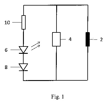
[0019] Figure 1 shows a circuit according to the invention.
[0020] Figure 2 shows the circuit according to the invention complemented by a
switch
which is actuated by the integrated circuit.
[0021] Figure 3 shows the circuit according to the invention complemented by a
switch
which switches in time-controlled fashion, independently of the
integrated circuit.
[0022] Figure 4 shows the circuit according to the invention, wherein a switch
is
contained in the integrated circuit.
[0023] Figure 1 shows the circuit according to the invention. The circuit
consists of a
parallel circuit of a coil 2 and an integrated circuit 4, for example an RFID
chip, wherein
the integrated circuit 4 is connected to the coil 2 via its operating voltage
connectors. In the
coil 2 a voltage is induced by an external electromagnetic field of a
terminal. The induced
CA 02961103 2017-03-13
voltage in the coil 2 serves for supplying energy to the circuit. Further, the
coil 2 also
serves for contactless data transmission between the integrated circuit 4 and
the terminal
not represented. In principle, also a contact-type interface can be present,
however which is
not represented for reasons of clarity. In parallel to the integrated circuit
4 a series
connection is represented, which consists of a light emitting diode 6, a diode
8 and an
ohmic resistor 10, wherein the diode 8 and the resistor 10 are optional
components. The
coil 2, the integrated circuit 4 and the light emitting diode 6 are
substantial for the
invention.
[0024] To avoid excessively high voltages in the reverse direction at the
light emitting
diode 6 which can lead to the destruction of the light emitting diode 6,
according to the
invention, a shunt regulator, which is not represented, but is usually
contained in the
integrated circuit 4, regulates the operating voltage of the integrated
circuit 4 to a value so
that trouble-free operation is possible and an excessively high voltage in the
reverse
direction of the light emitting diode 6 is prevented.
[0025] In a preferred embodiment, it is important that sufficient energy is
present for the
operation of the integrated circuit 4, and not for the operation of the light
emitting diode 6.
This means that when the circuit according to the invention is approached to a
terminal
with an electromagnetic field, sufficient energy will be made available first
to the
integrated circuit 4 to start its operation. Upon approaching the circuit
according to the
invention further to the terminal, in connection with an increase of the
available energy
and, ultimately, an increase in the voltage made available by the coil 2, in
dependence on
the conducting state voltage of the light emitting diode, sufficient
electrical energy will be
available starting at a certain distance from the terminal so that the light
emitting diode
lights up. The value of the conducting state voltage of the light emitting
diode 6 therein
depends on its emitted wavelength and/or luminous color and the material of
the light
emitting diode 6. It cannot occur therefore that the integrated circuit 4
cannot start its
operation, in particular in a weak electromagnetic field, for example at a
great distance to
the terminal, since the energy is consumed by the light emitting diode 6. This
can be
CA 02961103 2017-03-13
6
achieved by a light emitting diode 6 with a conducting state voltage in the
forward
direction that is as high as possible.
[0026] The diode 8 serves for further increasing the voltage difference
between the light
emitting diode 6 and the integrated circuit 4 and to thus ensure that the
integrated circuit 4
will be supplied with sufficient energy first for starting its operation,
before the light
emitting diode 6 begins to light up. The diode 8 can be a normal diode, a
Zener diode, a
light emitting diode or any other suitable diode, for example. Other
components and
circuits are possible as well which fulfill the same purpose as the diode 8.
To the diode 8,
further diodes can be connected in series as needed, which is not represented.
[0027] The ohmic resistor 10 serves for limiting current and thus to adjust
the brightness of
the light emitting diode 6 by limiting the flowing electrical current. The
resistor 10 can
have valuesof up to 1000 ohm, for example. As construction type, all suitable
construction
types are conceivable, for example as a discrete component of an SMD
construction type
or as a printed conductive path with distributed resistance.
[0028] The coil 2 in an advantageous embodiment consists of at least two
individual coils,
wherein a ferrite is arranged in at least one of the two coils. The two coils
are laid out for
the same resonance frequency. Therein, one of the coils can be employed to
supply the
integrated circuit 4 and the other coil can be used to supply a load. As a
load, there come
into question for example a heating coil for thermochromic inks for making
information
contained in the card visible, for example for personalization, or at least
one light source,
for example a LED, OLED, or other functional load.
[0029] The ferrite allows for the terminal to make respond or activate a coil
with a lower
response field strength than would be possible without the ferrite. Thus an
optimization of
the response field strength of at least one coil can take place in accordance
with
specifications or standards or a customer's requirements. For example, an RFID
functionality must meet the relevant standards, wherein the LED 6 can be given
lower
priority. Thus the ferrite makes it possible that one single coil can be
supplied with energy
CA 02961103 2017-03-13
-
7
independently of the area of the respective coil enclosed in each case and
independently of
the other coil, wherein at the same time the response field strength of the
respective coil is
reduced and/or the terminal can work with a lower field strength in order to
supply the
respective coil with energy for the operation of the integrated circuit 4 or
of a functional
load.
[0030] The coils can be arranged so that they are arranged on one common or on
different
levels of the card. The coils can be arranged as partially or fully
overlapping coils, coils
arranged side by side or coils arranged within one another.
[0031] The two coils can have the same or a different size. This means that
one coil
encloses the entire surface of the card, for example a so-called full-size
coil, or one coil
encloses only a part of the entire surface of the card, such as a so-called
half-size coil.
[0032] The coils can be formed of one or multiple layers. For example one of
the coils can
have one layer and the other one can have two layers. In a multi-layer coil,
for example an
insulating layer is arranged between the windings of the coil.
[0033] When more than one coil is used, it is not absolutely required for the
coils to be
arranged on the same side of a substrate, for example an inner foil layer of a
card, or on the
same substrate, but they can be arranged on different sides of the substrate
or on different
substrates.
[0034] The two coils have at least one winding each, wherein the two coils can
have an
equal or a different number of windings.
[0035] The ferrite can be arranged within a coil as a foil or by means of a
printing process
or in a different suitable manner. Through the arrangement of a ferrite in at
least one of the
two coils, the coil within which the ferrite is arranged is supplied with
energy
preferentially, since the ferrite quasi collects the field lines.
CA 02961103 2017-03-13
8
[0036] By varying the geometry and the electromagnetic properties, for example
the
choice of material or the processing parameters of the ferrite, such as when
printing, it is
also possible to adjust the resonance frequency and other electrical
properties of the
respective coil. Therein, the ferrite can be smaller than the respective coil
within which the
ferrite is arranged, of similar size or also larger than the associated coil.
[0037] The arrangement of the ferrite in the card is independent of the
position of the coils
in principle. The ferrite can be arranged on the same substrate surface as one
of the coils or
can be arranged on a back side of the substrate or also on a different foil
layer within the
card. Further, the ferrite can also be applied to the outside of the card. The
advantageous
effect of the ferrite is that the ferrite influences the ratio of the
inductances of the two coils,
so that a response field strength of a coil within which the ferrite is
arranged is reduced and
thus improved.
[0038] As a further advantageous embodiment example, it is expedient to
combine the
LED 6 with optical glitter bodies. When employed in chip cards, introduced
optical glitters
bodies, such as reflective metal or glimmer particles, for example pigments
preferably in
the form of small flakes, can result in an optically visible image by the
flakes having the
effect of a bright lighting up with a so-called glitter effect, i.e. a
punctual optical reflection
instead of an areal, optical scattering.
[0039] By employing the LED 6 as a point light source inside the card in
connection with
the glitter bodies there will result brightly lighting up points. Daylight or
artificial light
each represent a diffuse optical light source which produces only diffuse
optical reflections
with a very low optical intensity. This results in a significantly different
picture through
active illumination of the card by means of the LED 6 in comparison to a
diffuse optical
light source, such as represented by the daylight, for example. Thus, the
combination
consisting of the LED 6 in the card and glitter bodies is suitable as a
security feature.
[0040] As a further embodiment of the invention, to a transparent card
material can with
reflective metal or glitter particles also a fluorescent dye can be added for
converting light
CA 02961103 2017-03-13
9
of the built-in LED 6 to a light with a longer wavelength, which can be
recognized by a
viewer from the outside.
[0041] In a further embodiment, the optical glitter bodies or scattering
bodies have a
different refractive index than the surrounding card material in order to
obtain optical
effects, such as reflection, refraction or scattering. The optical glitter
bodies or scattering
bodies can be employed as a security feature, for example as a security strip,
or as an
optically noticeable effect.
[0042] The optical glitter bodies can be applied to at least one foil before a
final step for
manufacturing the card, for example by means of lamination, wherein said foil
is arranged
for example on the inside of the card after the manufacture of the card. The
optical glitter
bodies can be applied on the foil over the full surface by means of a coating
or only over
part of the surface, for example by means of a printing process.
[0043] As another embodiment example, the optical glitter bodies can be
integrated for
example in a material of a foil, for example by addition of the optical
glitter bodies into an
extruder for manufacturing the foil. The foil with the integrated optical
glitter bodies can
later be arranged in the card over the full surface or in the form of strips
of foil with the
integrated optical glitter bodies in any desired orientation, wherein the
preferred orientation
is in the longitudinal or transverse direction.
[0044] As optical glitter bodies further the following materials can be used,
such as
chopped glass fibers, so-called microfiber, spheres of glass or plastic which
are solid or
hollow. In particular hollow spheres have a strong optical effect through the
trapped air.
The smaller the sphere diameter is, the higher is the stability, wherein the
optical effect is
improved with a larger diameter. For example, the diameter of the spheres is
in the range
of! to 200 gm.
[0045] Generally, the material introduced in the form of optical glitter
bodies can also be
colored, i.e. either it is colored only on the surface or the material as a
whole is colored.
CA 02961103 2017-03-13
Possible further exemplary variants are that the material has one or multiple
colors and/or
is transparent and at the same time UV-fluorescent.
[0046] For the case that hollow spheres are employed, said hollow spheres can
also be
filled with a magnetic ink, such as e-ink. The filling of the sphere can
consist of a colored
liquid and contain electrically charged or magnetic nanoparticles of a
different color. Thus,
a security feature is obtained that can be switched externally or internally.
[0047] In the finished card the introduced materials in the form of optical
glitters bodies
can be recognizable to a viewer. The optical glitter bodies can be
recognizable from one or
both sides of the card when the glitters bodies are arranged in unprinted
regions of the card
and light shines through the card from a back side of the card. Further, the
materials
introduced in the form of glitter bodies can be recognizable in the finished
card in a printed
area when light from a light source shines through under the printed surface.
[0048] This is for example the case when the LED 6 is arranged below a printed
card
surface. Alternatively, the introduced glitter bodies are recognizable on the
front side or
back side of the card. As a further alternative, the optical glitter bodies
are recognizable on
an edge of the card, when for example light is coupled from the outside into a
light guide
of the card and the light is transmitted via the light guide to a different
side and coupled out
again there.
[0049] In a finished card the introduced materials in the form of optical
glitters bodies can
thus be visible upon viewing in transmitted light, upon viewing in incident
light, by
activation of a light source present in the card body, for example the LED 6,
or by light
present in the card body which is coupled into or passed on to transparent
layers or regions
for example, wherein the light is passed on by means of areal or strip-shaped
light guides
for example.
[0050] As light guide strip foils can be used. The strip foils here can have
one or multiple
layers. Further, identical strip foils can be laid in the card in parallel or
at an angle, for
CA 02961103 2017-03-13
11
example in crossed fashion. Furthermore, strip foils can be laid which both
contain optical
glitter bodies and do not contain optical glitter bodies. Here, the strip
foils which contain
optical glitter bodies are at least partially transparent, wherein the strip
foils without optical
glitter bodies are opaque or transparent. Further, there is the possibility
that a viewing
window is formed on the card surface in the region where the strip foils
intersect.
Alternatively, a viewing window can also be formed in the edge region.
[0051] Figure 2 shows the circuit according to the invention complemented by a
switch 12
which is actuated by the integrated circuit 4. The switch 12 is shown here as
a separate
component that is actuated or activated by a signal of the integrated circuit
4. The switch
12 is for example actuated by the integrated circuit 4, as soon as the
integrated circuit 4 has
started its operation and sufficient energy is available to operate also the
light emitting
diode or to have the light diode 6 indicate a result of a processing, for
example.
[0052] Figure 3 shows the circuit according to the invention complemented by a
switch 12
which switches independently of the integrated circuit 4, for example in time-
controlled
fashion.
[0053] Figure 4 shows the circuit according to the invention, wherein a switch
12 is
contained in the integrated circuit 4.
[0054] There are now different application cases for the circuit according to
the invention
with a switch 12.
[0055] In the case of an automatic transaction confirmation the entire energy
received in
contactless fashion is first employed for the integrated circuit 4, e.g. an
RFID chip, to carry
out a transaction. Since the total energy received in contactless fashion is
supplied to the
integrated circuit 4, the distance between the circuit according to the
invention and a
terminal can be maximized.
CA 02961103 2017-03-13
12
[0056] After completion of the transaction, the light emitting diode 6 is
activated via the
switch 12 and the completed transaction is thus indicated. Therein the switch
12 can either
be actuated directly by the integrated circuit 4 or independently of the
integrated circuit 4,
after the expiration of a certain time that is permitted as the maximal
transaction time by
relevant standards, for example.
[0057] In a different application case, a lighting up of the light emitting
diode 6 signals
that the circuit according to the invention, which is arranged on a secure
element, e.g. a
credit card, is disposed in an electromagnetic field of a terminal. Upon
actuation of a
switch 12 disposed in the secure element and actuated by a user, the
integrated circuit 4
receives the energy required to execute a transaction. During the execution of
the
transaction, the light emitting diode 6 is turned off by the integrated
circuit 4, so that it is
ensured that the integrated circuit 4 and the light emitting diode 6 do not
have to share the
available energy.
[0058] Here, the light emitting diode 6 is an example for all other possible
types of a load,
such as an electroluminescent display or a heating resistor.
[0059] In a particular application, the switch 12 can be used to operate the
light emitting
diode 6 in pulsed fashion. This is possible when the current-limiting resistor
10 is chosen
correspondingly low and the light emitting diode 6 is operated in pulsed
fashion by
opening and closing the switch 12 at a high frequency. The human eye then
perceives the
light from the light emitting diode 6 to be brighter than perceived in non-
pulsed operation
at the same energy consumption. By the pulsed operation of the light emitting
diode 6 it is
thus possible either to save energy at the same brightness of the light
emitting diode 6
perceived by the human eye, in which case more energy is available to the
integrated
circuit, or the brightness of the light emitting diode 6 perceived by the
human eye can be
increased at the same energy consumption.
[0060] Further, by suitably adapting the time length of pulse duration and
pulse pause
despite different distance from the terminal and related different
electromagnetic field
CA 02961103 2017-03-13
13
strength, the brightness of the light emitting diode 6 can be regulated so
that the brightness
will always be perceived as equally bright by the human eye in a certain
distance range of
the card from the terminal.
CA 02961103 2017-03-13
14
List of reference numbers
2 coil
4 integrated circuit, e.g. an RFID chip
6 light emitting diode
8 diode
ohmic resistor
12 switching element