Note : Les descriptions sont présentées dans la langue officielle dans laquelle elles ont été soumises.
I
NONDESTRUCTIVE, ABSOLUTE DETERMINATION OF
THICKNESS OF OR DEPTH IN DIELECTRIC MATERIALS
[0001] This invention was made with government support under contract
numbers FA865008C5306 and FA865012C5109 awarded by the United States
Department of Defense (United States Air Force). The United States Government
has certain rights in this invention.
TECHNICAL FIELD
[0002] This invention pertains to an apparatus and method for the non-
destructive determination of the depth of features in a dielectric material,
the
thickness of a dielectric material, and the use of thickness information so
determined in nondestructive evaluation (NDE) of bulk dielectric materials.
BACKGROUND ART
[0003] There is an unfilled need for improved, nondestructive means to test
bulk
dielectric materials for flaws, defects, irregularities, and other features;
and
particularly to determine the absolute thickness of bulk dielectric materials
when
given access to only one side of a part under inspection. Additionally, there
is an
unfilled need for improved, nondestructive means to determine variations in
the
density (or porosity) when the thickness of a bulk dielectric material is
known. For
example, there is an unfilled need for improved, nondestructive means for
examining dielectric materials in three dimensions, volumetrically, and
measuring
both thickness and changes in thickness. For a manufactured dielectric
component
that has been in service for some time, the remaining thickness is often
important
as an indicator of the component's remaining life; but it can be difficult to
measure
thickness when only one surface of the component is accessible. Density can
also
be a major indicator of the serviceability of manufactured dielectric
components,
because the density often relates directly to the strength of the component.
The
dimensions of a manufactured part are often known or are easily measured, but
it is
more difficult to determine density and variations in density. There is an
unfilled
Date Recue/Date Received 2021-08-11
2
need for improved means for the nondestructive determination of density and
changes in density of a bulk dielectric material when its thickness is known.
[0004] For example, there is an unfilled need for enhanced, nondestructive
means for measuring the remaining wall thickness in dielectric tanks and
pipes.
(This invention has numerous applications, and is not limited to the
inspection of
tanks and pipes.)
[0005] Modern chemical processing often involves the use of components made
of dielectric materials. Common dielectric material product forms include
fiber
reinforced plastic (often called "fiberglass" or "FRP") pipes and vessels.
These
materials are also commonly used in modern infrastructure, such as drinking
water
and waste water processing. There exists an unfilled need for improved means
to
measure the thickness of such materials nondestructively, especially for means
that
may be employed while the produce remains in-service, and where there is
access
to only one side of the dielectric component. (This invention has numerous
applications, and is not limited to the inspection of FRP.)
[0006] Due to the corrosive or abrasive nature of the fluids that are often
used in
various processes, the wall thickness often diminishes over time as a direct
result of
service-induced degradation. These service-induced thickness changes are
difficult
to detect nondestructively through conventional means.
[0007] It is highly desirable that a testing method should be
nondestructive, and
that it should be usable whether a facility is running or idle. Furthermore,
because
the access space outside the component can be limited, and the geometry of a
component can be complex, any portion of the detection machinery that must be
in
contact with the component (or in the vicinity of the component) should be
small
enough to accommodate the available space and geometry.
[0008] When the component to be tested is made of metal, then well-
established
ultrasonic inspection techniques can be used. However, ultrasonic inspection
cannot be used effectively for reinforced dielectric materials, because the
structural
fibers scatter nearly all sound energy, and return little usable signal. The
mesh or
Date Recue/Date Received 2021-08-11
3
fabric of a composite material so strongly scatters and disperses ultrasonic
waves
that the resulting reflection is extremely noisy. Eddy current measurements or
magnetic measurements do not work well in these materials either, because they
do
not conduct electricity.
[0009] Neither
is radiography particularly helpful. X-ray radiography can be used
to detect changes in bulk density or to detect changes in thickness, but it
requires
access to both sides of the component under inspection. This renders X-ray
radiography ineffective for in-service inspection of many components.
[0010] Another example of an unfilled need for improved methods to measure
density lies in the field of engineered ceramic composites. In such composites
both
the reinforcing fibers and the matrix are made of a ceramic material.
Typically, the
fibers are woven or otherwise arranged into a support structure into which the
matrix is deposited by chemical methods. The matrix is typically deposited
iteratively. The chemical reaction that results in the deposition occurs in
sequential
steps, with each step depositing additional ceramic material into the
interstices
between reinforcing fibers. Since the location of the fibers and the outer
boundary
of the part do not change, the porosity of the part decreases (and its density
correspondingly increases) with each iteration. When the
parts are highly
engineered and their physical dimensions are closely controlled, the physical
thickness, measured in inches or mm, is generally known within close
tolerances.
Because the strength of a part is typically a function of its density, it
would be highly
desirable to have improved nondestructive means to measure density. Ultrasonic
methods are not effective for determining density in such materials, due to
the
scattering of sound waves by the reinforcing fibers. Neither can eddy current
or
magnetic methods be used, as the ceramic composites are bulk non-conductors.
Although changes in density can be detected by radiography, the changes of
interest in ceramic composite applications are typically too small to be
resolved by
conventional radiography. Additionally, radiography requires access to both
sides of
the part, for that reason is not an acceptable method in many circumstances.
Date Recue/Date Received 2021-08-11
4
[0011] An overview of microwave testing techniques is given in A. Bahr,
Microwave Nondestructive Testing Methods (1982).
[0012] Several microwave nondestructive testing techniques are disclosed in
A.
Lucian et al., "The Development of Microwave NDT Technology for the Inspection
of
Nonmetallic Materials and Composites," pp. 199-232 in Proceedings of the Sixth
Symposium on Nondestructive Evaluation of Aerospace and Weapons Systems
Components and Materials (San Antonio, TX 1967).
[0013] J. Kurian et al., "Microwave Non-Destructive Flaw/Defect Detection
System for Non-Metallic Media Supported by Microprocessor-Based
Instrumentation," J. Microwave Power and Electromagnetic Energy, vol. 24, pp.
74-
78 (1989) discloses a method for detecting defects in a tire by measuring
transmission of microwaves from a dipole transmitting antenna inside the tire,
through the treads of the tire, with transmission detected by a linear array
of
detectors. Differential rates of transmission were correlated with changes in
thickness or with defects.
[0014] C. Howell et al., The Use of Low Cost Industrial AM-CW 'Microwave
Distance Sensors' for Industrial Control Applications (no date) discloses a
microwave distance sensor to measure distances to an object from about 15
centimeters to about 6 meters away, by measuring the phase angle of a returned
amplitude-modulated microwave signal reflected from the object.
[0015] United States patent no. 3,278,841 discloses a microwave flaw
detection
system, particularly for use with large, solid-propellant rocket motors.
Microwaves
were transmitted from inside the propellant, reflected off a metal casing, and
detected by a receiver displaced from the microwave transmitter.
Irregularities in
the strength of the received signal were correlated with cracks or other flaws
in the
propellant.
[0016] United States patent no. 4,520,308 discloses a system for measuring
the
thickness of a dielectric material by measuring the phase shift of microwaves
Date Recue/Date Received 2021-08-11
5
transmitted along a microwave strip line conductor adjacent to the material
whose
thickness is being measured. See also United States patent no. 4,123,703.
[0017] United States patent no. 2,999,982 discloses a Doppler-effect-based
method for microwave detection of inhomogeneities in compact materials such as
polished glass. Relatively high scanning speeds were used to produce a Doppler
effect. In the one example given, the relative speed of the glass versus the
detector
was 650 centimeters per second.
[0018] United States patent no. 3,144,601 discloses a method for microwave
detection of inhomogeneities in non-conducting materials such as glass sheets
and
plates. Detection was performed by simple measurement of the echoes of the
reflected microwaves; by measuring losses in intensity following transmission
through the object; or by mixing incident and reflected waves to create beats,
particularly when the material being examined was traveling (i.e., detecting
Doppler
shifts in the frequency of the reflected microwaves).
[0019] United States patent no. 3,271,668 discloses the use of microwaves
to
measure the rate of progressive attrition from a surface of a body of a solid
dielectric material; for example, measuring the burning profile in a solid
rocket
motor. Microwaves were transmitted through the fuel (or other material), the
surface of which reflected some of the microwaves back to a detector. The
relative
phase of incident and reflected microwaves varied as the distance from the
microwave transmitter to the surface of the burning fuel changed, allowing the
distance to the surface of the fuel to be determined as a function of time.
[0020] United States patent no. 4,707,652 discloses a technique for
detecting
impurities in a bulk material by measuring changes in the scattering of
microwave
radiation incident on the bulk material.
[0021] United States patent no. 4,514,680 discloses a method for detecting
knots in lumber, by transmitting microwaves through the lumber from two
sources of
the same intensity, but with a 180-degree phase shift. Transmitted microwaves
are
detected on the opposite side of the lumber. If the lumber is knot-free, there
is a
Date Recue/Date Received 2021-08-11
6
null in the microwave field at the detectors, but if a knot is present the
phase and
amplitude of microwave radiation at the detectors are altered.
[0022] United States patent no. 4,581,574 discloses a method for
determining
the average dielectric constant of a dielectric material having a conductive
surface,
by transmitting microwaves from two transducers into a sheet of the material,
and
making measurements of the energies of reflected microwaves. By measuring
average dielectric constants along a plurality of paths in the plane of the
sheet,
locations of variations within the sheet may be identified.
[0023] United States patent no. 4,274,288 discloses an acoustic,
interferometric
method for measuring the depth of a surface flaw such as a crack.
[0024] United States patent no. 4,087,746 discloses a method for
determining
optical anisotropy in a dielectric material by measuring changes in the
polarization
of microwaves transmitted through the material.
[0025] United States patent no. 6,172,510 discloses the probing of targeted
portions of a layered material by microwave radiation focused onto the
targeted
portion by adjustment of antenna position and orientation establishing a
single
oblique incidence path for reflection of antenna emitted probing radiation.
Signal
measurements of the radiation along the oblique incidence path are obtained to
provide for evaluation and detection of defects in the targeted portion of the
structure being probed.
[0026] A. Khanfar et a/., "Microwave near-field nondestructive detection
and
characterization and disbands in concrete structures using fuzzy logic
techniques,"
Composite Structures Elsevier UK, vol. 62, pp. 335-339 (2003) discloses a near-
field microwave nondestructive testing technique for disbond/crack detection
and
evaluation in a concrete structure. The frequency of operation and standoff
distance
could be optimized to achieve maximum sensitivity to the presence of a
disband,
which is viewed as an additional layer and which changes the properties of the
effective reflection coefficient (phase and magnitude). The change depends on
the
thickness and location of the disbond. Multiple frequency measurements could
be
Date Recue/Date Received 2021-08-11
7
used to obtain disbond location and thickness information. A fuzzy logic model
was
described relating the phase of reflection coefficient, frequency of
operation, and
standoff distance to the disbond thickness and depth.
[0027] S.
Ganchev et al., "Microwave detection of defects in glass reinforced
polymer composites," Proc. SPIE ¨ International Society for Optical
Engineering
USA, vol. 2275, pp. 11-20 (1994) discloses the use of microwaves for defect
and
flaw detection in glass reinforced polymer composites. The standoff distance
and
the frequency were studied as means of increasing detection sensitivity.
[0028] A prior
microwave method for the nondestructive testing of dielectric
components employs virtual standing waves. See U.S.
Patents 6,359,446,
7,777,499, 6,653,847, and 8,035,400 These methods, while effective for
detecting
and characterizing thickness or density changes over a small range (plus or
minus
1/4 of the wavelength "A" in the material being inspected), can give ambiguous
results in some circumstances. Several different values for the thickness or
density
can correspond to a single value of the measured output. Despite
the
improvements represented by these earlier methods, the 8,035,400 patent
frankly
acknowledged: "There can be ambiguity in interpreting an interferometric
signal, as
points within the specimen that are spaced an integral number of half-
wavelengths
apart may not initially be distinguished from one another, due to the
identical phase
of the waves reflected from such points (where the wavelength in question is
that
within the material, which generally differ from the wavelength in air or
vacuum,
depending on the index of refraction)." One solution proposed was that "if a
frequency is chosen to reduce the number of wavelengths needed to traverse the
thickness of the specimen, one may enhance the sensitivity at a selected depth
range with minimal ambiguity. In the special case where the specimen thickness
is
less than (preferably substantially less than) half the wavelength, then the
imaging
may be optimized for a single, very narrow band of the thickness within the
specimen." However, no solution was proposed for the more general problem of
resolving these ambiguities when the thickness of the specimen can be several
multiples of a wavelength. There is an unfilled need for improved testing
methods
Date Recue/Date Received 2021-08-11
8
that can resolve such ambiguities in measurements of bulk dielectric
thickness,
density, or features.
[0029] See also
U.S. Patents 5,539,322, 5,574,379, 5,216,372, 6,005,397,
3,025,463, 4,344,030, 4,754,214, 5,384,543, 7,190,177; Japanese patent
abstract
61274209; and published international application W09710514.
DISCLOSURE OF INVENTION
[0030] I have
discovered an improved high resolution method and apparatus to
determine depth and thickness in bulk dielectric materials. I have discovered
a
novel way to resolve the ambiguity in depth or thickness that was left
unresolved in
earlier interferometry-based nondestructive measurement techniques. The novel
method can unambiguously resolve depth and thickness with high precision.
Monochromatic radiation, preferably microwave radiation, more preferably
microwaves in the 5-50 gigahertz frequency range, is used to interrogate a
sample.
The microwaves are partly reflected at each feature where the dielectric
constant
changes (e.g., to measure thickness changes as the microwave beam encounters
the back wall of the specimen under inspection, with varying distance between
the
back wall of the specimen and the microwave source and detectors). In a
preferred
embodiment, the apparatus comprises a single microwave source, and two or more
detectors. The distance(s) between the detectors (and therefore their phase
relationship) is known (or can be measured). A portion of the transmitted beam
is
combined with the signal reflected by the specimen under inspection. These two
signals have the same frequency, but may differ in amplitude and phase. The
signals combine at the location of each detector to produce an interference
pattern,
a pattern that changes as the thickness of the specimen changes, or as the
position
of the specimen changes relative to the detector. For each
detector, the
interrogating radiation may be thought of as a sinusoidal (or quasi-
sinusoidal)
standing wave. If one used only a single detector, then the relationship
between the
detector output and the sample thickness would produce ambiguous thickness
measurements, with identical output values occurring every 1/4 wavelength in
thickness (or A/4) as the thickness changes (assuming that all other
parameters
remained unchanged). Simply repeating the measurements with multiple detectors
Date Recue/Date Received 2021-08-11
9
does not resolve the ambiguity, regardless of the spacing of the detectors
(whether
spacing is measured in distance or in phase).
[0031] As used in the specification and claims, unless context clearly
indicates
otherwise, terms such as "thickness," "depth," and the like should be
understood as
referring in the first instance to distance as measured in units of the
wavelength (A)
of the microwave energy that is used to perform the inspection, where the
wavelength is the effective wavelength in the material under inspection, which
in
general will differ from the wavelength in air (or vacuum). Conversion to
other
convenient units (e.g., mm, cm, in) may easily be performed where desired.
Fundamentally, an initial determination in accordance with the present
invention
determines the number of unit wavelengths in the material being inspected,
with
conversion into measurements in other units being secondary or derived from
the
number of wavelengths thus determined.
[0032] I have discovered a method of "combining" the output of multiple
detectors into a novel phase plot, a phase plot that can resolve the ambiguity
that is
otherwise inherent in measurements of thickness, depth, etc. A simple example
will
illustrate: Consider an embodiment with two detectors spaced A/4 apart (based
on A
in air). (The technique can be generalized to detector numbers greater than
two,
and to detector spacings other than A/4. In general, increasing the number of
detectors will improve resolution.) For the purposes of this illustration, the
distance
between the microwave source (and detectors) to the front surface of the
specimen
will be held constant. Thus the phase relationship between the front surface
and
the detectors is constant. Additionally, the contribution of the front surface
reflection
to the signal at each detector remains constant in both phase and amplitude,
even
as the thickness varies. The output signals from the two detectors vary
periodically
in the thickness domain, either sinusoidally or quasi-sinusoidally. For an
individual
detector, this periodic behavior produces an ambiguity in the inferred
thickness.
The present invention allows this ambiguity to be resolved. It is preferred
that the
spacing between the two detectors be chosen so that the absolute value of one
detector's output is a maximum when the output of the other detector is
halfway
between its own maximum and minimum. (This point may or may not be equal to
Date Recue/Date Received 2021-08-11
10
zero, depending on where the null is set in a particular case.) Alternatively,
it is
preferred that the spacing between two detectors be chosen so that the
absolute
value of the slope of a line tangent to the standing wave is a maximum on one
detector when the slope of a line tangent to the standing wave for the other
detector
is zero. To illustrate, in a hypothetical ideal case where the output signal
is precisely
sinusoidal, the preferred spacing between the detectors would be such that the
phase difference between the two detectors is 900 + (n x 180 ), where n is an
integer (which may be positive, negative, or zero).
[0033] Apparent changes in thickness, measured in units of the microwave
wavelength in the material, can result either from actual changes in dimension
(e.g.,
measured in inches or centimeters), or from density changes (which cause
changes
in refractive index and therefore wavelength). Unless context clearly
indicates
otherwise, as used in this disclosure and in the Claims, the term "thickness"
should
be understood to refer to the apparent thickness of a material, as measured in
units
of wavelength of the interrogating radiation. In other words, the "thickness"
is the
apparent thickness, which can be a function both of the actual dimensions of
an
object, and its density and refractive index, which may vary as a function of
position.
The invention provides an apparatus and method for the non-destructive
determination of specimen thickness (or feature depth), measured in units of
wavelength within the inspected material, and the use of thickness information
so
determined in nondestructive evaluation (NDE) of bulk dielectric materials.
The
refractive index of a material depends on its chemical composition. The
refractive
index also varies as a function of the density, even with a constant chemical
composition. The dependence of refractive index upon density results in a
change
in the wavelength of the electromagnetic energy as it propagates through
regions of
varying density. Thus the ability to determine changes in the position of a
standing
electromagnetic wave in a specimen, the dimensions of which are known, permits
determination of the refractive index, and hence the density (or porosity,
which is
inversely related to the density).
[0034] The detector may be scanned relative to the specimen at any desired
speed, and the scanning speed need not even be uniform. The novel detection
Date Recue/Date Received 2021-08-11
11
technique is not based on Doppler-shifts in frequency, which result from
motion, but
rather is based on interference between reflected and reference microwaves
that
have substantially the same frequency, where the interference is caused by
changes in location (independent of motion per se).
[0035] The novel technique can detect thickness changes and changes in
dielectric constant (which in dielectrics may, for example, result from
changes in
density or porosity), in essentially any dielectric materials. The technique
can also
be successfully used on composite materials containing conductive components,
but whose construction makes them overall nonconductors -- for example, carbon
fiber composites.
[0036] The novel method and apparatus have been successfully tested in a
prototype embodiment. The microwave transmitter/detector was small, and
readily
suited for use in environments in which access space may be limited.
[0037] The computed thickness value from the processed signal (from the
detectors) may be plotted as "Z" in a 3-dimensional plot, where "X" and "Y"
are
Cartesian coordinates on the surface of a specimen, to produce a map of
thickness.
(Other coordinate systems may also be used in lieu of an orthogonal Cartesian
system, as convenient for the shape of the particular specimen being
inspected, for
example cylindrical coordinates, toroidal coordinates, spherical polar
coordinates,
etc.) In an alternative embodiment, a fourth dimension may be added to a plot,
using color palette variations to indicate the presence of defects in the
specimen.
[0038] If
desired, one may determine whether a through-thickness inspection is
feasible for a particular specimen with a particular transducer by placing the
transducer against one surface of the specimen and moving an object on the far
side of the specimen. If the microwave energy fully penetrates the specimen, a
change in the position of the object on the far side of the specimen should
produce
changes in the observed transducer signal. In such a case, a thickness
measurement should be possible.
Date Recue/Date Received 2021-08-11
12
[0039] In accordance with an embodiment of the present invention there is
provided a method for non-destructively and unambiguously measuring the
thickness of a bulk dielectric material, or measuring the depth of a feature
in a bulk
dielectric material, or both. The method comprises the steps of: (a)
generating
microwaves from a microwave source, wherein the microwaves have substantially
constant frequency; (b) directing a first portion of the generated microwaves
to the
material to produce a standing wave of reflected microwaves; wherein the
standing
wave is a function of the wavelength of the microwaves, of the distance from
the
source to the nearest surface of the material, and of the distance from the
source to
farthest surface of the material or the distance from the source to a feature
within
the material; (c) mixing the reflected microwaves, in each of at least two
different
detectors, with a second portion of the generated microwaves to produce an
interference signal for each of the detectors; wherein the detectors are
spatially
displaced from one another; wherein the interference signal is a function of
the
thickness of the material, or a function of the depth of a feature within the
material,
or both; and wherein there is a phase difference between the different
detectors at
the frequency of the microwaves as a consequence of the spatial displacement
between the detectors; (d) determining, for each of one or more locations on
or in
the material, a point in a phase plane space whose coordinates correspond to
the
magnitude and sign of the interference signals that are produced at each of
the
detectors for each of the one or more locations; and (e) correlating, for each
of the
one or more locations on or in the material, the point that is determined in
the phase
plane space with a unique thickness for the material at each location, or with
a
unique depth for a feature within the material, or both.
[0040] In accordance with a further embodiment of the present invention
there is
provided an apparatus for non-destructively and unambiguously measuring the
thickness of a bulk dielectric material, or measuring the depth of a feature
in a bulk
dielectric material, or both. The apparatus comprises (a) a generator of
microwaves
of substantially constant frequency; wherein the generator is adapted to
direct a first
portion of the generated microwaves to the material to create a standing wave
of
reflected microwaves; wherein the standing wave is a function of the
wavelength of
Date Recue/Date Received 2021-08-11
13
the microwaves, of the distance from the source to the nearest surface of the
material, and of the distance from the source to farthest surface of the
material or
the distance from the source to a feature within the material; (b) at least
two
different detectors displaced spatially from one another, wherein each of the
detectors is adapted to add the reflected microwaves with a second portion of
the
generated microwaves to produce an interference pattern for each of the
detectors;
wherein the interference pattern is a function of the thickness of the
material, or a
function of the depth of a feature within the material, or both; wherein there
is a
phase difference between the different detectors at the frequency of the
microwaves
as a consequence of the displacement between the detectors; and (c) a computer
programmed to determine, for one or more locations on or in the material, a
point in
a phase plane space whose coordinates correspond to the magnitude and sign of
the interference signals that are produced at each of the detectors for the
one or
more locations; and to correlate, for each of the one or more locations, the
point that
is determined in the phase plane space with a unique thickness for the
material at
each location, or with a unique depth for the feature within the material, or
both.
BRIEF DESCRIPTION OF THE DRAWINGS
[0041] Figure 1 depicts a phase plane plot showing detector A and B output
voltages as (X,Y) data pairs in two dimensions, for a case with two detectors
and a
detector spacing of A/4. This plot is for a hypothetical, idealized case in
which no
attenuation in the material occurs.
[0042] Figure 2 depicts a phase plane plot showing detector A and B output
voltages as (X,Y) data pairs in two dimensions, for a case with two detectors
and a
detector spacing of A/4. This plot is also for a hypothetical, idealized case,
but it
represents a more realistic system in which microwave energy is lost in the
inspected material by attenuation (as a function of what is often termed the
"loss
tangent" of the material).
[0043] Figure 3 depicts schematically the distance from the Phase Plane
spiral
to its center as a function of sample thickness.
Date Recue/Date Received 2021-08-11
14
[0044] Figure 4 depicts an experimentally measured thickness domain plot
using two detectors.
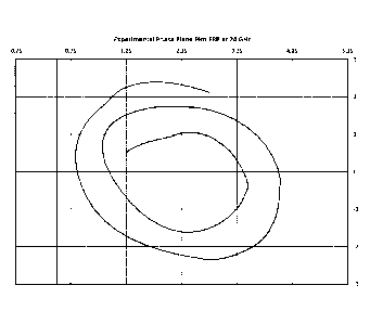
[0045] Figure 5 depicts an experimentally measured phase plane plot.
[0046] Figure 6 depicts schematically, in cross section, a fiberglass wedge
that
was used for testing the prototype embodiment over a range of depths.
[0047] Figure 7 depicts schematically a prototype embodiment of an
apparatus
in accordance with the present invention.
MODES FOR CARRYING OUT THE INVENTION
[0048] Substances such as fiberglass that produce noisy reflection patterns
in
ultrasonic techniques may be inspected at low noise levels with the novel
microwave technique. For example, the novel technique readily detects
thickness
changes in fiberglass, or in ceramic composites.
[0049] There are many potential fields of use for the invention. As one
illustration, the invention may be used to inspect fiber-reinforced plastic
(FRP) pipe.
Commercially available FRP pipe is a complex composite structure, typically
containing many layers of varying composition, density, and dielectric
constant.
When microwaves are directed towards an FRP pipe, reflections return from all
interfaces between materials of different dielectric constant. The returning
signal is
a superposition of many different waveforms, essentially identical in
frequency, but
generally differing in phase and amplitude. In general, the full thickness of
the
material is inspected, and all interfaces upon which the microwaves impinge
contribute to the returning waveform. The present invention is capable of
measuring the remaining thickness in such materials with a high degree of
precision, accuracy, and repeatability.
[0050] Mixing a portion of the outgoing radiation with the reflected
waveform
results in a complex standing waveform. (The
waveform is "standing," i.e.,
unvarying, similar to a vibrating string, so long as the relative positions of
the
transducer and the specimen remain unchanged, but in general it will vary as
those
Date Recue/Date Received 2021-08-11
15
positions vary.) The standing waveform that corresponds to a single detector
passes from the inspection device (transducer), then usually through an
intervening
medium such as air, and then into the specimen. As the waveform passes through
components of the specimen having differing indices of refraction, the
wavelength
changes, while the frequency remains constant. The higher the index of
refraction,
the slower the propagation of electromagnetic energy, and the shorter the
wavelength becomes.
[0051] When the
output signals of the two detectors are plotted against one
another (not necessarily as a direct function of time, nor necessarily as a
direct
function of distance, but against one another) ¨ for example with the voltage
at the
"A" detector as the "X" value and the voltage at the "B" detector as the
corresponding "Y" value in an (X,Y) data pair ¨ then the resulting plot will
generally
be an ellipse (or quasi-ellipse), as depicted schematically in Figure 1. (The
ellipse
could even be a circle if the relative sensitivities of the two detector
outputs were
identical.) Each time the thickness of the material changes by 1/2 A, the
(X,Y) data
point repeats and passes around the ellipse. This combination of the output
from
two detectors extends the unambiguous range for measuring thickness by a
factor
of 2, from 1/4 A to 1/2 A. If a straight line is drawn from any point on the
ellipse to the
center, the angle from that line to the x-axis (or any other fixed line
passing through
the origin) corresponds to the thickness within a range of 1/2 A.
[0052] Actually, the idealized elliptical phase plot shown in Figure 1 is
oversimplified since it disregards the loss of microwave energy that also
occurs with
changes in thickness. For a particular type of dielectric material, the
attenuation
increases as a function of sample thickness. As depicted in Figure 2, the
attenuation losses convert the theoretically lossless phase plane ellipse of
Figure 1
into something more similar to an elliptical spiral. These losses actually are
beneficial for the measurement process, because they provide additional
information that can be extracted. In the phase plane spiral of Figure 2, note
that
the values of (X,Y) do not repeat. The phase plane spiral curve does not cross
itself, meaning that the periodic ambiguity in thickness depicted in Figure 1,
which
exists when only the relative phase of multiple detectors is considered, is
eliminated
Date Recue/Date Received 2021-08-11
16
by plotting the (X,Y) coordinates represented by the signal from the multiple
detectors in phase plane space, with the amplitude of the signal decreasing
with
increasing sample thickness. (Actually, as shown in Figure 5 of Appendix A of
priority application 61/882,288, even with the novel phase plane analysis
there can
still sometimes be regions of ambiguity arising from internal reflections of
microwaves from boundaries. Even
when such complications exist, most
measurements in the phase plane analysis still produce unambiguous
determinations of thickness / depth.)
[0053] The
present invention is capable of determining thickness unambiguously,
using a combination of phase and amplitude measured by multiple detectors when
the specimen is irradiated from a common microwave source.
[0054] Figure 7
depicts schematically a prototype embodiment of an apparatus
in accordance with the present invention. The prototype apparatus comprised a
transducer with a single microwave source (transmitter) and two detectors. The
detectors output two channels of SIGNAL information (not shown). The detectors
were separated by approximately 0.12 inch (0.30 cm) in the direction of
propagation, corresponding to approximately 1/4 wavelength. The SIGNALs from
the two detectors were transferred to signal conditioning electronics, where
they
were amplified, filtered, and conditioned prior to being sent to an analog-to-
digital
converter (ADC). There were two position encoders, "X-Pos" and "Y-Pos" (not
shown), the outputs of which were also sent to the ADC. The ADC transmitted
digital data, containing SIGNAL information for both channels, and X and Y
location
data, to a processing computer, which then created images for chosen regions
of
interest.
[0055] In the
prototype apparatus, the output voltage from the 2 separate
detectors was combined in a display and analysis computer. In
future
embodiments, this data processing will be performed in a dedicated processor
located on the transducer itself.
Date Recue/Date Received 2021-08-11
17
[0056] A fiberglass wedge was constructed for prototype testing; a cross
section
is illustrated schematically in Figure 6. The wedge was scanned to confirm
that
acceptable data could be collected, and that the prototype embodiment worked
as
expected.
[0057] The Transducer
[0058] A preferred transducer was a microwave transceiver based on a Gunn
diode. See, e.g., B. Hale (ed.), The 1989 ARRL Handbook for the Radio Amateur,
pp. 32-57 & 32-58 (66th ed., 1988); The Microwave Gunnplexer: An Introduction
(various authors, no date); M/A-COM Semiconductor Products, Varactor Tuned
Gunnplexer Transceiver "Front End" (1985); Microwave Associates, Varactor
Tuned
Gunn Oscillator Transceivers for Commercial Applications (1977). The
transducers
that were used in prototype embodiments of the invention were tunable 10, 25,
or
35 gigahertz transceivers (frequencies could be higher or lower if desired,
e.g., 5 -
50 GHz). The transceiver could be used with or without a waveguide section.
The
detector had two microwave frequency diodes incorporated as part of the
assembly.
The detector diodes were located inside the outgoing radiation beam, between
the
aperture and the front surface of the transducer housing. The transducer was
frequency-stable, and required only a 5-10 Volt DC power supply to produce the
desired microwave output energies. It was mounted in a housing, which could
either be moved by hand, or in future embodiments will preferably be moved by
an
automated inspection device (a robot).
[0059] The transducer included mechanical means to control the stand-off
distance; the stand-off distance is preferably held constant. The transducer
was
connected to signal processing electronics, data acquisition hardware, and an
imaging and analysis computer via a multiple-conductor cable.
[0060] The transducer was also connected to a position-encoder system for
determining the X and Y position of the transducer. The position encoder
outputs
were fed to the computer for use in imaging and analysis of the specimen.
[0061] Signal Processing and Power Supply
Date Recue/Date Received 2021-08-11
18
[0062] In the
prototype embodiment, the detection diodes were located at fixed
positions within the path of the outgoing microwave beam, so that the output
signal
maintained a constant amplitude and frequency as seen by each detection diode.
Alternatively, the positions of the detection diodes could be made variable,
independent of varying the stand-off distance. Microwaves radiated from the
transducer to the specimen being tested. Each time the microwave beam came to
an interface between materials of different dielectric constants (e.g., the
interface
between air and the specimen, or the interface between the bulk specimen and a
flaw or feature within it), a portion of the microwave energy was transmitted,
and a
portion was reflected. The portion that was reflected depended on the angle of
incidence, the difference in the dielectric constants between the materials
(which is
related to the index of refraction), the surface texture, and other factors.
Some of
the reflected portion of the interrogating beam returned to the transducer,
where it
was detected by the detector diode(s). The reflected signal and the
transmitted
signal were of identical frequency, but (in general) differed in both
amplitude and
phase. These simple sinusoids or quasi-sinusoids added together (were mixed)
at
the detecting diode(s), to produce a DC voltage that changed as the sample (or
portion of sample) under inspection changed. In most specimens there are many
interfaces, producing many reflected signals. However,
regardless of the
complexity of the reflected signal, the detector diode(s) output produced a
constant
DC voltage when the position of the transducer relative to the specimen and
the
interrogating frequency were both held constant. This constant DC voltage is
sometimes referred to as the "SIGNAL." The "SIGNAL" may comprise multiple
components, from multiple detectors.
[0063] The
SIGNAL was transferred to signal processing electronics via a wired
connection. The observed SIGNAL was typically on the order of 1-100 millivolts
at
the input of the signal processing electronics. The SIGNAL was converted from
analog to digital form by the data acquisition system described earlier. The
analog
SIGNAL was digitized for maximum resolution of the SIGNAL voltage.
[0064] Routing
the SIGNAL directly to the data acquisition system would have
diminished the resolution for extremely small defects that the intrinsic
frequency
Date Recue/Date Received 2021-08-11
19
stability and low noise of the transducer would otherwise permit. An amplifier
was
therefore included in the signal processing components, prior to the ADC. The
amplifier improved SIGNAL resolution by a factor greater than 100, while
maintaining an acceptable signal-to-noise ratio.
[0065] The data acquisition system supported eight differentially-connected
analog input channels, each with its own negative signal connection. At least
two
analog channels were used to input amplified SIGNAL. Additional digital
channels
were used for input from the X and Y position encoders. In general, it is
preferred to
collect position information for both the X and Y positions of the transducer.
However, it sometimes suffices to collect position information from a single
position
encoder. For example, when collecting data for a specimen having the shape of
a
right circular cylinder, the transducer may revolve radially around the
cylinder while
progressing axially down the cylinder at a known rate. Then the Y position is
a
direct function of the X position, and a single position encoder may suffice.
[0066] When the data from a scan over multiple locations is displayed
graphically at an appropriate scale, the resulting image shows thickness
changes in
the specimen. Typically, the collected dataset contains far more detail than
is
conveniently represented in a single image. The regions of interest are
therefore
selected, and an image is created by changing the scale and color (or gray
scale)
gradient for the SIGNAL for a clear visual display of the features of
interest. The
stand-off spacing is selected to obtain the depth resolution desired, which is
a
function of the frequency of the microwaves, and the index of refraction of
the
specimen. When a transducer with multiple detectors is used (rather than a
single
detector), then the number of scans may be reduced, as multiple images
optimized
at different depths may be created with data from a single scan.
[0067] The power supply for the microwave generator comprised a regulated,
low-voltage power supply between 5 and 12 VDC, capable of supplying current
sufficient to drive the Gunn diode. The 5-12 volts were delivered to the
transducer
housing, where power was delivered to the transducer. The same power supply
was configured to provide the required voltages for the amplifiers, position
Date Recue/Date Received 2021-08-11
20
encoders, and data acquisition system. Power for the data acquisition system
could
also be provided by the notebook computer via the USB interface.
[0068] Signal Analysis and Determination of Thickness
[0069] The novel technique is based, in part, on the principle that
interfaces
between materials with different dielectric constants (including, for example,
overall
thickness changes) act as microwave reflectors. When a scan is made by
measuring the SIGNAL at different X and Y positions, and the data are used to
create an image, these thickness changes can be displayed directly (as in a
thickness map of the specimen).
[0070] During scanning with the prototype device, information was
simultaneously gathered for values of the two SIGNAL channels, the X location,
and
the Y location. These data were processed by computer to produce a two-
dimensional image of the SIGNAL.
[0071] Obstacles overcome by the present invention.
[0072] The distance from a point on the Phase Plane spiral to its center,
termed
the "vector magnitude," changes more-or-less exponentially with thickness
(becoming longer at lower thicknesses, and shorter at higher thicknesses ¨ see
Fig.
3). This ideal exponential behavior occurs when the effective channel gains
are
identical and the effective phase difference between the two detectors is
precisely
A/4 (A in air). Since a combination of vector magnitude and phase angle is
used to
determine thickness unambiguously, ideally the transducer is positioned so
that the
effective phase angle between detectors is A/4.
[0073] If the microwave propagation could indeed be described accurately as
a
simple plane wave propagation, then the optimum distance between the two
detectors (in the direction of propagation) would simply be A/4. However, when
an
actual transducer was built with a simple A/4 displacement between the
detectors
and tested, the observed results were not as expected. The propagation of
microwaves inside a finite transducer is in fact neither an idealized
spherical wave
Date Recue/Date Received 2021-08-11
21
front, nor an idealized planar wave front, but instead is a complex hybrid
between
these two idealized cases. As a result, the optimum distance between the
detectors
is not simply A/4, as one might initially expect. Instead, the optimum
distance may
be empirically determined for a particular wavelength and a particular
waveguide.
When the detectors are optimally positioned, the vector magnitude varies
approximately exponentially with the thickness, and does not oscillate
substantially
as the thickness changes.
[0074] An additional complication is that the Phase Plane plot is truly
symmetric
only when the effective gains used to amplify the signals from all detectors
are
equal. However, unlike for the case for incorrect physical placement of the
detectors, when different gains are used the unequal gain ratios can be
corrected in
post-processing.
[0075] With previous microwave inspection techniques, it has sometimes been
necessary to adjust the "null" or offset voltage of a detector signal to
prevent signal
saturation and clipping. When the null voltage is changed for either or both
detectors, the center of the phase plane plot will move as well. This
complication
has made it difficult or impossible to determine thickness unambiguously using
prior
microwave inspection techniques, because for any real sample only a very small
portion of the phase plane spiral is available. (Indeed, if the thickness does
not
change, only a single point is known.) If the location of the center is not
known,
then the vector magnitude cannot be calculated and the thickness cannot be
determined. By contrast, in the current invention the null or offset voltages
are
preferably maintained constant, so that the center of the phase plane spiral
is
known, and the vector magnitude and thickness can be determined unambiguously.
[0076] A preferred method for practicing the invention is to plot points in
phase
plane space as described above, and to correlate those points with unique
distances empirically. However, those of skill in the art will recognize that
other
methods of achieving the same result are mathematically equivalent to the
preferred
method. For purposes of the present specification and claims, any
mathematically
Date Recue/Date Received 2021-08-11
22
equivalent method is considered to be identical to the preferred method, and
to be
within the scope of the invention as defined.
Date Recue/Date Received 2021-08-11