Note : Les descriptions sont présentées dans la langue officielle dans laquelle elles ont été soumises.
CA 2963665 2017-04-10
TWO-PHASE THREE-LEVEL CONVERTER AND CONTROLLER THEREFOR
Related Applications
This application claims the benefit of the filing date of U.S. Application No.
62/321,027, filed on
April 11, 2016, and of U.S. Application No. 62/473,464, filed on March 19,
2017, the contents of which
are incorporated herein by reference in their entirety.
Field
The invention relates to DC-DC converters. More particularly, the invention
relates to multilevel
buck converters, and to controllers and methods for operating such converters.
Background
Non-isolated DC-DC converters are widely used in modern electronic equipment.
These
converters are directly built right next to the load, and are also referred to
as point-of-load (POL) power
supplies. With increasing demand to miniaturize voltage regulators for
computers and
telecommunication products, high power density POL converter topologies are
highly desirable. The
inductor in a conventional buck converter occupies a large portion of the buck
converter's space. It is
difficult to reduce the size and weight of the inductor. For example, in
current POL power modules,
inductors occupy most of the substrate space such that they are the most
significant barrier to
increasing power density.
Increasing the switching frequency is a common and simple way to reduce the
inductance
required for a POL buck converter. A drawback of this approach is that the
power loss will be increased
and the switches will overheat. Also, increasing the switching frequency
beyond tens of MHz in a non-
integrated POL buck converter is impractical since a very small duty cycle is
needed to provide very low
output voltage (usually 0.5-1.6v) for modern microprocessors. A very small
duty cycle limits the
maximum switching frequency. The single phase three-level buck converter shown
in Fig.1A is a
potential candidate for replacing the conventional buck converter in high
power density POL converters
1
CA 2963665 2017-04-10
because the operating frequency can be doubled. More capacitors need to be
added to such a single
phase three-level buck converter to further increase the operating frequency
(e.g., a four-level buck
converter), but the extra capacitors complicate the operation of the
converter.
When high output current is needed, multi-phase converters may be used to
improve the
efficiency of the entire system. For a conventional multi-phase buck converter
such as two-phase buck
converter shown in Fig.1B, the output current is not evenly shared by each
phase because of component
tolerance and various parasitic components on the printed circuit board (PCB)
tracks. Uneven output
current sharing will cause uneven thermal dissipation and will decrease
efficiency of the converter.
Thus, auxiliary circuits and components are needed to share the output current
evenly, which increases
the cost of the converters and also complicates their control.
In a POL application, most loads require very low output voltage ranging from
0.5V to 3.3V. At
the same time, higher output voltages are also required, such as by USB ports
(5V), and for dynamic
voltage scaling. However, the voltage gain of the converters is small because
of the duty cycle
limitation. Accordingly, the maximum output voltage of the converters is
limited. This problem exists in
most three-level DC-DC converters.
Summary
According to one aspect of the invention there is provided a two-phase
asymmetrical three-level
buck converter, comprising: a first input terminal connected to a first common
terminal of a first switch
connected in parallel with a third switch; a first node connected to a second
common terminal of the
first and third switches, and to a first common terminal of a second switch
connected in parallel with a
fourth switch; a second common terminal of the second and fourth switches
connected to a second
node and a first terminal of a fifth switch; a first capacitor having a first
terminal connected to the first
node and a second terminal connected to a third node and a first terminal of a
sixth switch; a first
inductor having a first terminal connected to the second node and a second
terminal connected to a
main output terminal; a second inductor having a first terminal connected to
the third node and a
second terminal connected to the main output terminal; a common node connected
to a second input
terminal, a second terminal of the sixth switch, a second terminal of the
fifth switch, and a second
output terminal; and a second capacitor connected between the main output
terminal and the second
output terminal.
In one embodiment, the two-phase asymmetrical three-level buck converter may
comprise a DC
2
CA 2963665 2017-04-10
power supply connected across the first input terminal and the second input
terminal.
In one embodiment, the two-phase asymmetrical three-level buck converter may
comprise a
controller that provides a driving signal for each of the first to sixth
switches.
In one embodiment, the controller drives the first to sixth switches so that:
the first, second,
third, and fourth switches are driven with 90 phase difference from each
other; the fifth switch is
driven complementarily to the second and fourth switches; and the sixth switch
is driven
complementarily to the first and third switches.
In one embodiment, the controller drives the first to sixth switches so that:
the first, second,
third, and fourth switches are turned on and off once, sequentially, during
one switching cycle, wherein
a duty cycle of each of the first to fourth switches is prolonged such that
successive on times of the first,
second, third, and fourth switches overlap by a selected interval; and the
fifth switch and the sixth
switch are each turned on and off twice during a switching cycle; wherein the
fifth and sixth switches are
off during the overlaps of the on times of the first to fourth switches.
According to another aspect of the invention there is provided a controller
for a two-phase
asymmetrical three-level buck converter, comprising: an input that receives a
signal corresponding to
the converter output voltage or current; a circuit that generates a duty cycle
signal based on the sensed
output voltage or current; a driving circuit that generates gate drive signals
for switches of the
converter; wherein the converter is a two-phase asymmetrical three-level buck
converter; wherein the
controller drives the first to sixth switches so that: the first, second,
third, and fourth switches are
turned on and off once, sequentially, during one switching cycle, wherein a
duty cycle of each of the first
to fourth switches is prolonged such that successive on times of the first,
second, third, and fourth
switches overlap by a selected interval; and the fifth switch and the sixth
switch are each turned on and
off twice during a switching cycle; wherein the fifth and sixth switches are
off during the overlaps of the
on times of the first to fourth switches.
In one embodiment, increasing the selected interval of the overlap of the
successive on times of
the first to fourth switches increases the output voltage of the two-phase
asymmetrical three-level buck
converter.
According to another aspect of the invention there is provided a controller
for a series capacitor
buck converter comprising first and second control switches and first and
second synchronous rectifier
(SR) switches, the controller comprising: an input that receives a signal
corresponding to the converter
output voltage or current; a circuit that generates a duty cycle signal based
on the sensed output
voltage or current; a driving circuit that generates gate drive signals for
switches of the converter;
3
CA 2963665 2017-04-10
wherein the controller drives the switches so that: the first and second
control switches are turned on
and off once, sequentially, during one switching cycle, wherein a duty cycle
of each of the first and
second control switches is greater than 50% such that the on times of the
first and second control
switches overlap by a selected interval; and the first and second SR switches
are each turned on and off
once, sequentially, during a switching cycle, wherein each of the on times of
the first and second SR
switches coincides with an off time of one of the first and second control
switches; wherein the first and
second SR switches are off during the overlaps of the on times of the first
and second control switches.
In one embodiment, increasing the duty cycle above 50% increases the output
voltage of the
series capacitor buck converter.
According to another aspect of the invention there is provided a method for
controlling a two-
phase asymmetrical three-level buck converter, comprising controlling the
first to sixth switches so that:
the first, second, third, and fourth switches are turned on and off once,
sequentially, during one
switching cycle, wherein a duty cycle of each of the first to fourth switches
is prolonged such that
successive on times of the first, second, third, and fourth switches overlap
by a selected interval; and the
fifth switch and the sixth switch are each turned on and off twice during a
switching cycle; wherein the
fifth and sixth switches are off during the overlaps of the on times of the
first to fourth switches.
In one embodiment, increasing the selected interval of the overlap of the
successive on times of
the first to fourth switches increases an output voltage of the two-phase
asymmetrical three-level buck
converter.
According to another aspect of the invention there is provided a method for
controlling a series
capacitor buck converter comprising first and second control switches and
first and second synchronous
rectifier (SR) switches, comprising controlling the switches so that: the
first and second control switches
are turned on and off once, sequentially, during one switching cycle, wherein
a duty cycle of each of the
first and second control switches is greater than 50% such that the on times
of the first and second
control switches overlap by a selected interval; and the first and second SR
switches are each turned on
and off once, sequentially, during a switching cycle, wherein each of the on
times of the first and second
SR switches coincides with an off time of one of the first and second control
switches; wherein the first
and second SR switches are off during the overlaps of the on times of the
first and second control
switches.
In one embodiment, increasing the duty cycle above 50% increases an output
voltage of the
series capacitor buck converter.
According to another aspect of the invention there is provided a series
capacitor buck converter
4
CA 2963665 2017-04-10
comprising a controller as described herein.
Brief Description of the Drawings
For a better understanding of the invention, and to show more clearly how it
may be carried
into effect, embodiments will be described, by way of example, with reference
to the accompanying
drawings, wherein:
Fig. 1A is a circuit diagram of a single phase three-level buck converter
according to the prior art.
Fig. 18 is a circuit diagram of a two-phase buck converter according to the
prior art.
Fig. 2 is a circuit diagram of a two-phase asymmetrical three-level buck
converter according to
an embodiment of the invention.
Figs. 3-7 are circuit diagrams showing the first to fifth operating modes,
respectively, of the two-
phase asymmetrical three-level buck converter of Fig. 2, according to an
embodiment of the invention.
Fig. 8 is a timing diagram for the operating modes shown in Figs. 3-7, for the
two-phase
asymmetrical three-level buck converter of Fig. 2, according to an embodiment
of the invention.
Fig. 9 is a plot showing normalized output current ripple coefficient against
duty cycle for a
conventional two-phase buck converter and the buck converter of Fig. 2 when
the duty cycle is below
0.25, according to an embodiment of the invention.
Fig. 10 is a timing diagram for the two-phase asymmetrical three-level buck
converter of Fig. 2
operating under an input voltage boost control method, according to an
embodiment of the invention.
Figs. 11-18 are circuit diagrams showing working modes 1-8, respectively, of a
two-phase
asymmetrical three-level buck converter operating under the input voltage
boost control method,
according to an embodiment of the invention.
Fig. 19 is a circuit diagram of a series capacitor buck converter according to
the prior art.
Fig. 20 is a timing diagram for the series capacitor buck converter of Fig. 19
operating under an
input voltage boost control method, according to an embodiment of the
invention.
Fig. 21 is a circuit diagram showing working modes 1 and 3 for the series
capacitor buck
converter of Fig. 19 operating under an input voltage boost control method,
according to an
embodiment of the invention.
Figs. 22 and 23 are circuit diagrams showing working modes 2 and 4,
respectively, for the series
capacitor buck converter of Fig. 19 operating under an input voltage boost
control method, according to
an embodiment of the invention.
5
CA 2963665 2017-04-10
Figs. 24A and 24B are plots showing results of a simulation of a series
capacitor buck converter
operating according to the timing diagram of Fig. 20.
Figs. 25A and 258 are plots showing results of a further simulation of a
series capacitor buck
converter operating according to the timing diagram of Fig. 20.
Fig. 26 is a plot showing a relationship between duty cycle and output voltage
for a series
capacitor buck converter operating according to the timing diagram of Fig. 20.
Fig. 27 is a circuit diagram showing an implementation of a controller for a
series capacitor buck
converter, according to one embodiment.
Fig. 28 is a diagram showing gate logic elements for the controller of Fig.
27, according to one
embodiment.
Detailed Description of Embodiments
Throughout the drawings and the description, identical components have been
given the same
reference numerals.
Throughout the description and claims, the terms "first", "second", etc. are
used to differentiate
features or elements and not to indicate any particular relationship or
sequence among them.
For the purpose of this description, the term "RMS current" as used herein is
intended to refer
to root mean square current, \/,, refers to DC power supply voltage, Vci
refers to the first capacitor
voltage, VIA refers to the voltage across the first inductor, VL2 refers to
the voltage across the second
inductor, Vo refers to the output voltage, and R refers to load.
For the purpose of this description, the term "switch" is intended to refer to
a semiconductor
switch characterized by controllable conduction. The term "MOSFET" is used as
a non-limiting example
of all such semiconductor switches. An N-channel MOSFET is an example of such
a switch, wherein the
first terminal is the drain, the second terminal is the source, ard the
control terminal is the gate. The
control terminal of each semiconductor switch may be provided with its own
control signal. It will be
understood that other suitable devices, such as, for example, IGBT may be used
for the semiconductor
switches in the embodiments of the invention. In accordance with embodiments
described herein,
current in each switch may flow in both directions. This may be ensured or
enabled by, for example,
each switch being reversely connected in parallel with a diode. In accordance
with embodiments
described herein, such a switch may be, for example, an IGBT with a parallel
diode, or a MOSFET where
the parallel diode is inherent (i.e., the body diode).
6
CA 2963665 2017-04-10
One aspect of the invention relates to a two-phase asymmetrical three-level
buck converter and
control methods therefor. Fig. 2 shows a circuit diagram of a two-phase
asymmetrical three-level buck
converter according to one embodiment. Referring to Fig. 2, the circuit has
two input terminals, two
output terminals, six switches (T1, T2, T3, T4, T5 and T6), a first capacitor
C1, a first inductor L1, a second
inductor L2 and a second capacitor C2, and four nodes CN, N1, N2, N3, wherein
CN is the common node
(which may also be referred to as ground). One input terminal and one output
terminal are connected
together at the common node. The other output terminal is also referred to as
the main output
terminal MT. The load is shown as a resistor R connected across the main
output terminal and the
common node.
As shown in Fig. 2, the first switch T1 is connected in parallel with the
third switch T3, and the
second switch T2 is connected in parallel with the fourth switch T4. The
common first terminal of the
first and the third switches is connected to the first input terminal, and the
common second terminal of
the first and the third switches is the first node N1, which is connected to
the common first terminal of
the second and the fourth switches. The common second terminal of the second
and the fourth
switches is the second node N2, which is connected to the first terminal of
the fifth switch T5 and the
first terminal of the first inductor L1. The positive terminal of the first
capacitor C1 is connected to the
first node N1, and the negative terminal is connected to the third node N3 and
the first terminal of the
sixth switch T6. The positive side of a DC power supply is connected to the
first input terminal, and the
negative side of the DC power supply is connected to the second input
terminal. The first inductor L1 is
connected between the second node N2 and the main output terminal MT. The
second inductor L2 is
connected between the third node N3 and the main output terminal MT. The
second capacitor C2 is
connected across the main output terminal MT and the common node CN. The
second input terminal,
the second terminals of the sixth switch T6 and the fifth switch T5, and the
second terminal of the
second capacitor C2, are all connected together with the second output
terminal, which all together are
referred to as the common node CN.
Each of inductors L1 and L2, together with the second capacitor C2, forms an
LC filter.
In some embodiments, the two LC filters may be omitted. When the two LC
filters are omitted,
the output will be two pulse voltages.
In some embodiments, the second capacitor C2 may be omitted. When the second
capacitor C2
is omitted, the output will be constant current.
In this description, the term "switch group A" refers to the first switch T1
and the second switch
T2, and the term "switch group B" refers to the third switch T3 and the fourth
switch T4.
7
CA 2963665 2017-04-10
Another aspect of the invention relates to a method or operating the
embodiment of Fig. 2. An
example of a control method is shown in Figs. 3-7, in which the operation of
the circuit is presented as
five working modes. The timing diagram is shown in Fig. 8. This operating
method is referred to herein
as the "normal" operating method, or "normal" operation. Another operating
method of the
embodiment of Fig. 2 is described in Example 1, below.
Normal operation is described below with the following exemplary values: total
voltage of DC
power supply \fin is equal to 12 volts, the voltage Vo is half of Vr, (6
volts), the output voltage equals 2.5
volts and the switching frequency for each of the switches T1, T2, T3, and T4
is 300 KHz. In Figs. 3-7,
portions of the circuit shown with solid lines are working during that mode,
and portions shown with
dotted lines are off during that mode.
The voltage Vo equals half of Võ-, in this embodiment, which is a non-limiting
example. That is,
Vo and Vn are not limited to a particular relationship. Rather, the voltage
Vci may be chosen to be any
value between zero and V.
The potential on the common node CN is defined as ground potential. The
current or voltage
between the second node and the main output terminal forms a first phase
output, and that between
the third node and the main output terminal forms a second phase output. The
term "V1" refers to the
voltage supplied to the first inductor (between the second node N2 and the
common node CN), and
"V52" refers to the voltage supplied to the second inductor (between the third
node N3 and the
common node CN).
For the first working mode shown in Fig. 3, the current in L2 flows as
follows: DC4T14C14
L2-3R4DC. The first capacitor C1 is charged by the DC power supply. The
voltage V5w2 equals the DC
power supply voltage V,n minus the first capacitor voltage Vo. That is, V5w2 =
\tin - VG= 0.5Vn. At the
same time, there is a freewheeling loop for the first inductor L1. It is
T54L14R-4T5. The voltage V5wi
equals zero. That is, V5w1= 0.
For the second working mode shown in Fig. 4, the inductor L1 works in
freewheeling mode
through the following loop: T5->L1->RT5. The voltage \isi equals zero. That
is, V51 =0. The inductor
L2 also works in freewheeling mode through the following loop: T6->L24R4T6.
The voltage V5w2
equals zero. That is, V5w2 =0.
For the third working mode shown in Fig. 5, the current in L1 flows as
follows: C1-T231_14R4
T64C1. The first capacitor C1 is discharged. The voltage Vswi equals the first
capacitor voltage Vo.
That is, \ism. = VD.= 0.5V1n. The inductor L2 works in freewheeling mode
through the following loop:
T6--)L24R4T6. The voltage V5w2 equals zero. That is, V52 =0.
8
CA 2963665 2017-04-10
For the fourth working mode shown in Fig. 6, the inductor L1 works in
freewheeling mode
through the loop as follows: T54L1-->R4T5. The voltage Vi equals zero. That
is, Vswi =O. The current
in L2 flows as follows: DC4T3- C1L24R--)DC. The first capacitor C1 is charged
by the DC power
supply. The voltage Vsw2equals the DC power supply voltage V,n minus the first
capacitor voltage Vci.
That is, Vsw2= V - Vci =0.5Vin.
For the fifth working mode shown in Fig. 7, the current in L1 flows as
follows:
C14T44L14RT64C1. The first capacitor C1 is discharged. The voltage V51
equalsthe first
capacitor voltage Vci. That is, Vswi = Vci =0.5V,n. The inductor L2 works in
freewheeling mode through
the following loop: T6-)L24R4T6. The voltage Vsw2equals zero. That is, Vsw2
=O.
According to this embodiment, the two-phase asymmetrical three-level buck
converter works
alternately among the five above-mentioned working modes by controlling the on
and off states of each
switch to output the selected voltage.
Fig.8 shows the timing diagram for the switches in this embodiment during one
switching
period Ts. The four switches T1, T2, T3, and T4 are driven with 90 phase
difference from each other.
The switch T5 is driven complementarily to the switches T2 and T4, and the
switch T6 is driven
complementarily to the switches T1 and T3.
As shown in Fig. 8, switches in switch group A and switch group B are
interleaved. During the
first half period (from 0 to 0.5Ts), the switches T1 and T2 in switch group A
are on in turn and the
switches T3 and T4 in switch group B are off. During the second half period
(from 0.5Ts to Ts), the
switches T3 and T4 in switch group B are on in turn and the switches T1 and T2
in switch group A are off.
It is noted that in one period Ts, the switches in either switch group A or
switch group B turn on
only once but the operating frequency of the voltage \Ism. and V2 istwice.
This means that each
inductorL1, L2 operates at, e.g., 2 MHz when the four switches T1, T2, T3, and
T4 operate at 1 MHz. To
achieve the same operating frequency, the conventional single phase three-
level buck converter in Fig.
1A and the conventional two-phase buck converter in Fig. 1B must have double
the switching frequency
and each switch must turn on twice. Thus, the root mean square current in each
of the four switches is
reduced by half compared to the conventional three-level buck and two-phase
buck converters.
Accordingly, the conduction power loss in each switch is reduced.
Since the input voltage to the inductor of each phase is reduced and the
operating frequency is
twice the switching frequency, the inductance of a two-phase asymmetrical
three-level buck converter
as described herein is much smaller than that of the conventional two-phase
buck converter.
In this description, the term DATL is intended to refer to the duty cycle. It
is defined as the
9
CA 2963665 2017-04-10
percentage of on time of a switch in one switching period Ts. That is, LIT,
where T., refers to the
conduction time. The voltage conversion ratio is defined as V0/V. Using of the
principle of inductor
volt-second balance in Equation (1), the output voltage V. may be derived.
1r Ts
(v1,)= ¨ .1 v ,(t)dt = 0 (1)
T 0
s
Apply Equation (1) to the inductors L1 and L2 to get Equation (2).
(v11) = ¨1 .17 s v11 (t)dt = 0
T 0
,
i (2)
T
, 1 s
[(vL2 i = ¨j. vi , (t)dt = 0 o "-
,
Applying small-ripple approximation to Equation (2), Equation (3) is derived.
J(v11) = 2 . D A 1 [ (V, ¨ V,)+ (1 ¨ 2 . D477 )(¨V0)= 0
(v,,)= 2. D477 (V,õ ¨ V ¨ Võ) + (1-2. D47,,)(¨VQ)= 0 (3)
Simplify Equation (3) and solve the equation, leads to Equation (4), where the
ratio of V. to V,,, is
the voltage conversion ratio.
Vo = Vin = DA TL (4)
As shown in Fig. 8, the switches T1 and T2 or T3 and T4 do not overlap during
normal operation.
So the maximum duty cycle is 0.25. For 12V input, the maximum output voltage
is 3V.
As the output current of the two-phase asymmetrical three-level buck converter
is derived by
summing two phases of inductor current, the output current ripple in each
phase is at least partially
cancelled out, such that the inductor current ripple is reduced. Accordingly,
the LC filter requirement is
reduced.
The normalized output current ripple of the conventional two-phase buck
converter in Fig. 1B
may be expressed as Equation (5), where K is the ripple cancellation
coefficient, D is duty cycle and it is
defined as the magnitude ratio of the output current ripple Aio to inductor
current ripple AiL;
m=floor(2=D).
m m +1
2 . (D2 ) . ( D)
K = Ai', =
2 (5)
Ail D = (1¨ D)
CA 2963665 2017-04-10
For the two-phase asymmetrical three-level buck converter, the operating
frequency of each
inductor is twice the switching frequency. Thus, the duty cycle of the
inductor current is twice that of
the switches. Equation (6) gives the normalized output current ripple, where
m=floor(4-DATL).
m m+1
All
2 )=( 2D41/)
K = Ai" __ = 2 -(2D
(6)
AIL(1¨ )
D4I1 =
It can be seen from Equation (5) and Equation (6) that the amount of current
ripple cancellation
only depends on the duty cycle. Fig. 9 shows the normalized output current
ripple coefficient against
duty cycle for the conventional two-phase buck converter and a converter as
described herein when the
duty cycle is below 0.25 (i.e., output voltage is below 3V). It is noted that
POL converters usually have
very low duty cycle due to the low output voltage requirement.
Fig. 9 shows that a converter as described herein has lower output current
ripple coefficient
than the conventional two-phase buck converter. Therefore, the second
capacitor C2 may be
implemented with smaller capacitance.
It can be seen from the above five working modes that there are three
operating states of the
first capacitor C1 in one switching period. They are discharging, charging,
and floating. During the
steady-state, the first capacitor voltage Vci is fixed. Thus, the first
capacitor charge balance equation
and small-ripple approximation may be derived by Equation (7), where ILL and
In are DC values of in and
iL2; Dcharge and Ddischarge represent respectively the duty cycles of the
first capacitor charging and
discharging.
(ic) = Dcharg e = I Ll Ddischarge- = TS IL2 (7)
Equation (7) is simplified to (8) according to the first capacitor charge
balance, Dcharge=Dthscharge.
= /
Dcharge = I Ll = Dch,scharge L2 8)
It can be seen that In is always equal to In. Thus, a two-phase asymmetrical
three-level buck
converter as described herein has an inherent automatic inductor current
sharing mechanism. No extra
current sensing circuits and controllers are needed.
When the output current is reduced below the critical current level (e.g.,
lo=2A), the two-phase
asymmetrical three-level buck converter is operating in discontinuous
conduction mode. It is observed
that in only flows in one direction, but iL2 is able to flow in both
directions. The reason is that after in
falls to zero, it can continue to flow in the reverse direction and flow to
the negative terminal of the first
capacitor. But in is not able to continue to flow in the reversed direction.
Therefore, the DC current and
11
CA 2963665 2017-04-10
current ripple of each inductor are not equal.
The automatic current sharing mechanism weakens in discontinuous conduction
mode and may
become worse when taking into consideration component parameter variance. In
order to improve the
performance of the automatic inductor current sharing mechanism in
discontinuous conduction mode, a
control method according to another embodiment, referred to as the negative
circulating control
method is described.
According to the negative circulating control method, the two switches T5 and
T6 are kept on
when the currents in both inductors are going through zero, to keep them
decreasing to negative during
the rest of the freewheeling time. The switch T5 is driven complementarily to
the switches T2 and T4,
and the switch T6 is driven complementarily to the switches T1 and T3, as
shown in Fig. 8. The inductor
currents of the two phases are of the same DC value, so even inductor-current
sharing is achieved. In
this way, not only the performance of automatic inductor-current sharing
function remains as it does in
continuous conduction mode, but also no additional modification of the circuit
or controller is needed.
Another aspect of the invention relates to a controller that operates a two-
phase asymmetrical
three-level buck converter according to the methods described herein. The
controller may be
implemented in any combination of discrete and integrated components,
digitally or analogue, or in a
platform such as a field programmable gate array (FPGA), as known in the art.
Input Voltage Boost Control
The voltage gain (Vo/Vin) of three-level DC-DC converters, such as the example
described above,
is small because of the duty cycle limitation. Accordingly, the maximum output
voltage of such a
converter is limited. To address this issue, a control method referred to
herein as "input voltage boost
control" (IVBC) will now be described. As shown below, IVBC may be applied to
three-level DC-DC
converters to increase the output voltage level. Two embodiments of the IVBC
operating method are
described. In the first embodiment, described in Example 1, the IVBC method is
implemented in a two-
phase asymmetrical three-level buck converter as shown in Fig. 2. In the
second embodiment,
described in Example 2, the IVBC method is implemented in a two-phase three-
level buck converter
(also referred to as a series capacitor buck converter) as shown in Fig. 19.
Example 1
Fig. 10 shows the timing operation waveforms for each switch of a two-phase
asymmetrical
three-level buck converter, shown in Fig. 2, under the IVBC method. The
driving signal for each of the
12
CA 2963665 2017-04-10
four switches T1, T2, T3, and T4 has 90 phase difference from each other in
the normal operation mode
described above. However, under the IVBC method, each driving signal of the
four switches T1, T2, T3,
and T4 is prolonged to generate overlaps of the edges of the timing signals,
for example, T1 overlaps
with T2 and T4, T2 overlaps with T1 and T3, T3 overlaps with T2 and T4, and T4
overlaps with T3 and T1,
as shown in Fig. 10. The overlap regions are marked as s1, 53, 55, and S7 in
Fig. 10. The working states
in these regions are referred to as boost states since the current of inductor
L1 is boosted during that
time. In boost states, two series-connected switches are on at the same time.
The input voltage \isvs,1 to
the inductor L1 is V,õ instead of Vci for a short time. That is, the input
voltage Vswi to the inductor L1 is
increased so that the output voltage level is increased.
Under the IVBC method, there are eight working states in one switching period.
Each working
state is explained as follows with reference to Figs. 11-18:
State 1 (to-t1) in Fig. 11: The switches T1 and T4 are on. The current in L1
flows as follows:
DC4T1¨>T4-->L14134DC. The voltage V1 equalsthe DC power supply voltage Võ-,.
That is, Vsw1= V.
At the same time, the current in L2 flows as follows: DC4T1--)C14L24R--)DC.
The first capacitor C1 is
charged by the DC power supply. The voltage V5w2equals the DC power supply
voltage V,, minus the
first capacitor voltage Vci. That is, Vsw2= Vin - Vci=0.5V,n. Both L1 and L2
are charged.
State 2 (ti-t2) in Fig. 12: The switches T1 and T5 are on. The inductor L1
works in freewheeling
mode through the loop as follows: T54L14R--)T5. The positive terminal of
inductor L1 is grounded
through T5. The voltage V51 equalszero. That is, Vswi =O. At the same time,
the current in L2 flows as
follows: DC4T14C1¨>L24R4DC. The first capacitor C1 is charged by the DC power
supply. The
voltage V5w2equals the DC power supply voltage V,n minus the first capacitor
voltage Vci. That is, V5w2 =
VC1 0.5V,n. L2 is charged.
State 3 (t243) in Fig. 13: The switches T1 and T2 are on. The current in L1
flows as follows:
DC--)T14T2-4L1- R-)DC. The voltage V51 equalsthe DC power supply voltage Võ,.
That is, Vswi = Vin.
At the same time, the current in L2 flows as follows: DC-->T1--)C14L2R4DC. The
first capacitor C1 is
charged by the DC power supply. The voltage V52 equalsthe DC power supply
voltage Vin minus the
first capacitor voltage Vci. That is, V5w2= Vin - Vc1 = 0.5V,. Both L1 and L2
are charged.
State 4 (t344) in Fig. 14: The switches T2 and T6 are on. The current in L1
flows as follows:
C1-T2-L1-3R-T6-C1. The first capacitor C1 is discharged. The voltage Vswi
equals the first
capacitor voltage Va. That is, Vswi = Va. At the same time, the inductor L2
works in freewheeling mode
through the loop as follows: T64L24R4T6. The positive terminal of inductor L2
is grounded through
T6. The voltage V52 equalszero. That is, Vsw2=0. L1 is charged and L2
freewheels.
13
CA 2963665 2017-04-10
State 5 (t445) in Fig. 15: The switches T2 and T3 are on. The current in L1
flows as follows:
DC-T3-T2-L1-)R-DC. The voltage VL equals the DC power supply voltage \in,.
That is, \ism. = vin.
At the same time, the current in L2 flows as follows: DCT3-)C141_2--)R--->DC.
The first capacitor C1 is
charged by the DC power supply. The voltage Vsw2equals the DC power supply
voltage V., minus the
first capacitor voltage Vci. That is, V5w2= Vin - Vc1=0.5V, Both L1 and L2 are
charged.
State 6 (t5-t6) in Fig. 16: The switches T3 and T5 are on. The inductor L1
works in freewheeling
mode through the loop as follows: T54L14R4T5. The positive terminal of
inductor L1 is grounded
through T5. The voltage V51 equalszero. That is, \ism. =O. At the same time,
the current in L2 flows as
follows: DC-41-3->C14L24R4DC. The first capacitor C1 is charged by the DC
power supply. The
voltage Vsw2equals the DC power supply voltage Vin minus the first capacitor
voltage Va.. That is, Vsw2 =
Vin - VD. = 0.5Vn. L2 is charged.
State 7 (t647) in Fig. 17: The switches T3 and T4 are on. The current in L1
flows as follows:
DC4T34T44L14R--)DC. The voltage V51 equals the DC power supply voltage Võ-,.
That is to say, \ism.
= V,n. At the same time, the current in L2 flows as follows: DC4T34C1412-
>R4DC. The first capacitor
C1 is charged by the DC power supply. The voltage V5w2 equals the DC power
supply voltage Võ-, minus
the first capacitor voltage VG. That is, Vsw2= \fib - Vci=0.5Vn. Both L1 and
L2 are charged.
State 8 (t7-Ts) in Fig. 18: The switches T4 and T6 are on. The current in L1
flows as follows:
C14T44L14R->T64C1. The first capacitor C1 is discharged. The voltage V51
equals the first
capacitor voltage \in. That is, V5w1= WT. At the same time, the inductor L2
works in freewheeling mode
through the loop as follows: T64L24R4T6. The positive terminal of inductor L2
is grounded through
T6. The voltage Vsw2equals zero. That is, V5,2 =O. L1 is charged and L2
freewheels.
The duty cycle is expressed as in the above Equation (4) during normal
operation and DAL is not
greater than 0.25. Under the IVBC method, the duty cycle will be different
from the normal operating
method described above.
During State 4 and State 8, the inductor voltage VLL is Vc-Vo. It can be seen
from Fig. 10 that the
total duty cycle of State 4 and State 8 is0.5-2Dk during operation under IVBC.
Dbt is the duty cycle of
one boost state.
During boost states 1,3,5, and 7, VIA. is (Vin-V0). The total duty cycle of
these boost states is 4Dbt.
During freewheeling states 2 and 6, VIA is (¨V0). The total duty cycle of
these states is 0.5-2Dbt.
Next, using of the principle of inductor volt-second balance on inductor L1
derives Equation (9).
14
CA 2963665 2017-04-10
( VL -= (0.5 ¨ 2 = Di,,) = (V, ¨ V 0) + 4 = Dbt = (V,õ
(1¨ 0.5 + 2. Dbt ¨ 4 = D,õ ) = (¨Vo) = 0 (9)
By simplifying the Equation (9), Dbt is obtained in Equation (10).
2 V o , ¨ V
Dbt = ______________________ (1o)
8V, ¨ 417,
Referring to Fig. 10, the new duty cycle in extended output voltage mode is
0.25+Dbt.
Therefore, the duty cycle can be expressed in Equation (11).
V 1
when 0 < ,<
VV117 4
DAIL = (11)
2 V ¨ Võ V 1
o
_________________________ +0.25 when o
8V, ¨ 4 V, V 4
When Vo/Vir, is less than or equal to 0.25, the two-phase asymmetrical three-
level buck
converter works according to the normal operation described above. When Vo/V,,
is greater than 0.25,
the IVBC method provides output higher voltage.
As the output current splits, each phase carries half of the output current.
The two-phase
asymmetrical three-level buck converter according to the embodiments described
herein is particularly
useful for high output current applications.
Controller Implementation
An IVBC controller may be implemented using voltage-mode control, current-mode
control,
hysteresis control, etc. Controller components may include an error amplifier
that receives an input
based on sensed converter output voltage or current, an error amplifier that
produces an output error
signal, a PWM circuit that receives the error signal and generates a duty
cycle signal, and a gate drive
logic circuit that produces gate drive signals based on the duty cycle signal.
Of course, other
configurations may also be used. The controller may be implemented in any
combination of discrete
and integrated components, digitally or analogue, or in a platform such as a
field programmable gate
array (FPGA), as known in the art.
Example 2
In this example another embodiment of the IVBC operating method is described,
wherein the
method is implemented in a two-phase three-level buck converter (also referred
to as a series capacitor
CA 2963665 2017-04-10
buck converter) as shown in Fig. 19.
As shown in Fig. 19, the series capacitor buck converter consists of four
switches M1, M2, SR1,
and SR2. M1 and M2 are control switches and SR1 and 5R2 are synchronous
rectifier switches (or SR
switches). The drain of the first switch M1 is connected to the positive
terminal of the input voltage, Ni,r,
The source of the first switch is connected to both the positive terminal of
the flying capacitor Cf and the
drain of the second switch M2. The source of M2 is connected to the drain of
the third switch SR2 and a
first terminal of the first inductor L1. The source of the third switch 5R2 is
connected to a circuit
common, or ground. The drain of the fourth switch SR1 is connected to a first
terminal of the second
inductor L2 and the negative terminal of the flying capacitor Cf. The source
of SR1 is connected to
ground. Both of the second terminals of L1 and L2 are connected to the
positive terminal of an output
capacitor Co. The negative terminal of the output capacitor is connected to
ground. The load (RL) is
connected between the positive terminal of the output capacitor Co and ground.
Under the conventional control strategy, the maximum duty cycle of a series
capacitor buck
converter is limited below 0.50 and the maximum output voltage is 25% of the
input voltage. For
example, the maximum output is 3V for a 12V input. In practice, when
considering the power losses and
the dead time, the maximum output voltage will be below 3V for a 12V input.
However, as described herein, the IVBC method may be used to achieve higher
voltage gain for
a series capacitor buck converter. For example, with the IVBC method, a series
capacitor buck converter
can produce commonly used voltage levels, such as 3.3V and 5V, using a 12V
input voltage. A key
feature of the IVBC method is to introduce another voltage level at the input
of the inductor L1 (i.e.,
node B1 as shown in Fig. 19, Vsw1). The new voltage level is equal to Vin. In
other words, three voltage
levels are present at Vsw1: 0, 0.5Vin, and Vin.
Operation
The operating sequence of switches and typical waveforms under the IVBC method
are shown in
Fig. 20. It is assumed that the dead time is zero. Four operating states are
identified during each
switching period: State 1 (from to to t1), State 2 (from t1 to t2), State 3
(from t2 to t3), and State 4 (from
t3 to Ts). The circuit operation is described below with reference to Figs. 21-
23, wherein dashed lines
represent portions of the circuit that are not operating (i.e., the devices
are off) during each state.
State 1 (from tO to t1): The equivalent circuit is shown in Fig. 21. M1 is
turned on at to and M2 is
on. Therefore, M1 and M2 are on for this state. The first current path is Vint
M1-M2-L1-Co and
RL. The DC value of the inductor L1 current (in) is more than half of the load
current, which is different
16
CA 2963665 2017-04-10
from the conventional control strategy for the series capacitor buck converter
when only M1 or M2 is
turned on. The second current path is V,r,4M1-3Cf-->L24C0 and RL. The DC value
of the inductor L2
current (i1_2) is less than half of the load current, which is also different
from the conventional control
strategy. The steady state currents for inductors L1 and L2 are given in
Equations (17) and (18), below.
The flying capacitor Cf is charged by ii_2. During this period, the voltage at
B1 is Vs,,i=Vin. The voltage at
B2 is Vs,,2=Vin - Vcf. The value of Vcf may be calculated by Equation (12).
The inductor L1 voltage is Vin-Vo
and the inductor L2 voltage is Vin-Vcf ¨V.. Equation (13) gives the output
voltage value.
when 0 5_ D < 0.5
7
= ¨ (12)
V
V.
V ¨ -- when 0.5<D Ic_l
in D
when 0 D 0.5
V, =1 2 (13)
D(V,, ¨1/(7) when 0.5<D 1
State 2 (from t1 to t2): The equivalent circuit is shown in Fig. 22. M2 is
turned off at t = t1. SR2
is turned on immediately after M2 is turned off. M1 remains on. In this
operation state, one control
switch (M1) and one SR (5R2) are on. The first current path is: Vin->M1-
>Cf4L24Co and RL. The
amplitude of the current is the current of inductor L2 (4,2), which is less
than half of the load current.
The flying capacitor Cf is charged by i L2. The second current path is: SR2-L1-
Co and RL. The amplitude
of the current is the current of inductor L1 (in), which is more than half of
the load current. During this
period, the voltage at B1 is Vsw1=0. The voltage at B2 is Vsw2=Võ-,¨ Vcf The
inductor L1 voltage is -Vo and
the inductor L2 voltage is Vin-Vcf-Vo.
State 3 (from t2 to t3): The equivalent circuit is shown in Fig. 21. In this
state, t2 is half the
switching period Ts, t2 = 0.5Ts. At t=t2, SR2 is turned off and M2 is turned
on immediately after SR2 is
turned off. M1 is still on. In this operation state, both control switches (M1
and M2) are on. The first
current path is Vin4M1->M24L14Co and RL. The amplitude of the current is the
current of inductor
L1 (in), which is more than half of the load current and this is different
from the conventional control.
The second current path is Vin-M1-Cf-L2-*Co and RL. The amplitude of the
current is the current
of inductor L2 (1_2), which is less than half of the load current. The flying
capacitor Cf is charged by iL2.
The DC value of the inductor currents may be determined using Equations (17)
and (18). During this
17
CA 2963665 2017-04-10
period, the voltage at B1 is Vswi=Võ-,. The voltage at B2 is V2=V,õ - Vcf. The
inductor L1 voltage is Vin-Vo
and the inductor L2 voltage is Vin-Vcf ¨Vo.
State 4 (from t3 to Ts): The equivalent circuit is shown in Fig. 23. M1 is
turned off at t = t3. SRI
is turned on immediately after M1 is turned off. M2 remains on. In this
operation state, one control
switch (M2) and one SR (SR1) are on. The first current path is:
SR14Cf4M241..14Co and RL. The
amplitude of the current is the current of inductor L1 (in), which is more
than half of the load current.
The flying capacitor Cf is discharged by in. The second current path is: SR1-
L2-Co and RL. The
amplitude of the current is the current of inductor L2 (iL2), which is less
than half of the load current.
During this period, the voltage at B1 is Vi= Va. The voltage at B2 is Vs,,2=0.
The inductor L1 voltage is -
Vcf and the inductor L2 voltage is -Vo.
State 4 finishes at t = Ts when SR1 is turned off and M1 is turned on
immediately after SR1 is
turned off. The cycle repeats the operation in the next switching period.
Simulation results
Two simulations were conducted using PSIM (Powersinn Inc., Rockville, USA).
The following
circuit parameters were used: switching frequency 2MHz, L1 and L2 220nH, Co
600 F, and Cf 10p.F.
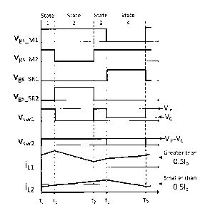
Fig. 24A shows the gate drive signals for four switches (M1, M2, SRI., and
SR2), and Fig. 24B
shows the simulation results for 12V input voltage and 3.3V output voltage.
The duty cycle is about
52.6% (i.e., larger than 50%). The output voltage is about 3.3V, as shown in
the last plot of Fig. 24B.
Fig. 24B shows the waveforms at key points. It is clearly shown that Vsw1 has
three voltage
levels, OV, about 6V (i.e., about half of the input voltage) and about 12V
(i.e., the input voltage). The
voltage Vsw2 has only two voltage levels, about OV and about 6V. Thus, under
the IVBC strategy, Vsw1
and Vsw2 have different waveforms, which is different from the conventional
control strategy where
the voltage waveforms for Vsw1 and Vsw2 are the same, and are merely 180
degrees out of phase.
Figs. 25A and 25B show simulation results for 12V input voltage and 5V output
voltage. Fig. 25A
shows the gate drive signals for four switches (M1, M2, SR1, and SR2). The
duty cycle is about 64.5%
(i.e., larger than 50%). Fig. 25B shows the waveforms at key points. It is
clearly shown that Vsw1 has
three voltage levels, OV, about 6V (half of the input voltage) and about 12V
(the input voltage). The
output voltage is about 5V, as shown in the last plot of Fig. 25B.
Summary of the IVBC Strategy
In the conventional PWM control method of the series capacitor buck converter,
the input
18
CA 2963665 2017-04-10
voltages to L1 are 0 and Vc (which is equal to half of Vin). In contrast, as
shown in the operating
principle above, the control scheme of IVBC changes the input voltage of one
of the inductors (L1) to 0,
Vc, and Vin. The new input voltage level of Vin enables the converter to
increase the output voltage
level. Within one switching period, during two states (State 1 and State 3),
the input voltage to L1
(Vsw1) is Vin. State 1 and State 3 may therefore be referred to as boost
states in the IVBC strategy. The
duration of a boost state is D ¨ 0.5. It is noted that a boost state occurs
when the duty cycle is higher
than 50%, or equivalently, the output voltage is higher than about Vin/4.
The control strategy with IVBC may be summarized as follows:
When the duty cycle is less than 50%, the operation of the IVBC strategy is
same as the
conventional control strategy.
When the duty cycle is larger than 50%, the IVBC strategy may be used to
achieve higher output
voltage.
Fig. 26 is a plot showing the duty cycle for commonly used output voltages
when the input
voltage is 12V. For example, a duty cycle of 0.416 is needed if the output
voltage is 2.5V. In this case,
the series capacitor buck converter (Fig. 19) operates according to the
conventional control mode. In
other words, Vsw1 will have only two voltage levels, OV and 0.5Vin. When the
required output voltage
is 3.3V, the duty cycle should be about 52.4%, and the circuit operates
according to the IVBC operating
mode. Vsw1 will have three voltage levels, OV, 0.5Vin, and Vin. It is noted
that the relationship given in
Fig. 26 is under ideal conditions. In practice, the required duty cycle will
be a little larger to compensate
for losses in the circuit and the dead times.
Inductor Current DC Value and Ripple
When the duty cycle is larger than 50%, IVBC operation is used and the
inductor ripple current
and DC current may be calculated using the following equations. Under IVBC
operation, the current of
L1 will rise faster during boost states since the input voltage to L1 is Vin
instead of V. The inductor
current ripple of L1,116 may be calculated using Equation (14), where tLi is
the charging time of inductor
current (i.e., tO to t1, or t2 to t3). In the equation Db = D - 0.5.
V V ¨V
Ai/1 =t/ I = _______________ (1 D)T, + 1"
" = 2D1, = T, (14)
L, L,
Equation (14) may be simplified and Aill calculated as follows:
170 = (1¨ D)T,
Ai I = (15)
L,
19
CA 2963665 2017-04-10
Similarly, the current ripple of Lz AO may be derived using Equation (16),
where tu is the
charging time of inductor current IL2 (i.e., t1 to t2). The current of L2
rises in a constant slope during
charging since the input voltage to L2 does not change during the boost state.
Ai
v 17, ¨ v, ¨17
1- , i ,õ , ¨ t1"- , , , , = D= T,
(16)
L, L,
The DC value of the inductor current L1 and L2 are given in the following two
equations:
Inductor L1 DC current value:
IL
when 0 ._ D 0.5
/ = 2 (17)
DI(( when 0.5<D ._-_ 1
Inductor L2 DC current value:
1/0 when 0 5_ D .. 0.5
L2 = 2
(18)
(1-D)Iõ when 0.5<D 1
For example, a duty cycle of 0.416 is needed if the output voltage is 2.5V and
the output current
is 10A. In this case In and 10 are approximately equal: In is 5A and lu is 5A.
When the output voltage is
3.3V, a duty cycle of 0.524 is needed. For this case, In is about 5.24A and
luis about 4.76A. Similarly, D
= 0.645 is needed for an output voltage of 5V, where In is about 6.45A and Lis
about 3.55A.
Implementation of a IVBC Controller
An IVBC controller may be implemented by modifying a conventional controller
for a series
capacitor buck converter. For example, controller components such as the error
amplifier and most of
the gate drive logic circuit may be employed in IVBC embodiments, such as
voltage-mode control,
current-mode control, hysteresis control, constant on time control, etc. Fig.
27 shows an embodiment
of a voltage-mode controller 210. In this embodiment, Vout (i.e., Vo) of a
series capacitor buck
converter 200 is sensed and fed into an error amplifier 212 and over-voltage
protection (OVP) circuit
214 of the voltage-mode controller 210. A PWM 216 receives an error signal Veõ
from the error
amplifier 212 and an output from the OVP circuit 214, as well as clock 217 and
soft-start 218 signals, and
generates a duty cycle D. A gate logic circuit 222 generates the required gate
drive signals for the gate
drivers 225 based on the duty cycle D and dead time 220.
In one embodiment the gate logic circuit operates as follows:
(1) The duty cycle D signal is used to control M1.
CA 2963665 2017-04-10
(2) A signal complementary to D (D_com) is generated and used to control SR1.
(3) A dead time is added between the M1 gate signal and the SR1 gate signal
when both M1 and
SR1 are off.
(4) The duty cycle D signal is delayed by half a switching period Ts (i.e.,
delayed by 1800 in phase).
The signal is referred to as D180 and is used to control M2.
(5) A signal complementary to D180 (D180_conn) is generated and used to
control 5R2.
(6) A dead time is added between the M2 gate signal and the SR2 gate signal.
(7) No 50% duty cycle limitation is added, so that the duty cycle can be
higher than 50%.
Fig. 28 is a diagram showing details of the gate logic circuit 222 according
to this embodiment.
It is noted that the conventional control strategy would include a 50% limit
circuit in the gate logic circuit
to limit the maximum duty cycle to 50%.
The duty cycle D for M1 and M2 are substantially the same. The duty cycle for
SR1 and 5R2 are
substantially same, and are 1 ¨ D. Also, there is no limitation on the maximum
value of the duty cycle of
the PWM signals. One group of PWM signals is used to drive M1 and its
complementary pair SR1, and
the delayed group of PWM signals is used to drive M2 and its complementary
pair SR2. Since the duty
cycle for switch M1 can be higher than 50%, the switch M2 can be turned on
even if the switch M1 is not
turned off. In this way, the PWM signals for M1 and M2 overlap as shown in
Fig. 20. The input voltage
to L1 will be VII-, during the boost state of operation. It will be
appreciated that this control strategy may
be implemented in any multi-phase multi-level converter topology, such as, but
not limited to, single-
phase three level converter (e.g., Fig. 1A), and three-phase four level
converter, to extend the
conversion ratio.
As described herein, the IVBC strategy increases the output voltage by
introducing different
input voltages (V5w1 and V5w2) to two inductors (L1 and L2). The input voltage
for L2 (V5w2) is same as in
the conventional control strategy when the maximum duty cycle is limited to
50%, and still has two
voltage levels, OV and 0.5Vin. The IVBC strategy introduces three voltage
levels for the input voltage of
L1 (Vsw1), OV, 0.5Vin, and vin. Therefore, the input voltages to the two
inductors, \ism. and Vs,õ,2, are
different. This feature of the IVBC strategy results in the higher output
voltage for the series capacitor
buck converter.
As compared with the conventional control strategy for the series capacitor
buck converter, the
proposed IVBC strategy extends the duty cycle to be higher than 50%, to
introduce a third voltage level
(V,n) at the input of the inductor L1 (V5w1) so that the output voltage can be
increased. In order to
achieve this, the duty cycles of M1 and M2 (two control MOSFETs) are extended
to above 50% so that
21
CA 2963665 2017-04-10
both M1 and M2 are conducting at same time, as shown in Fig. 20. The gate
drive for SR1 is
complementary to the gate drive of M1 so that when M1 is on, SR1 is off, and
when and M1 is off, SR1 is
on. Similarly, when M2 is on, SR2 is off and M2 is off, SR2 is on. In a
practical implementation, there is a
small dead time between M1 and SR1 when both M1 and SR1 are off. There is also
a small dead time
between M2 and SR2 when both are off.
In another embodiment, operation mode of the gate logic circuit is described
as follows:
(1) At the start of the switching cycle Ts, M1 is turned on. Immediately
before M1 is turned on, SR1
is turned off.
(2) M1 is on for a period Ton (Ton = D * Ts) and is then turned off.
Immediately after M1 is turned
off, SR1 is turned on.
(3) At the middle of the switching cycle (0.5Ts), M2 is turned on. Immediately
before M2 is turned
on, SR2 is turned off.
(4) M2 is on for a period Ton (Ton = D * Ts) and then is turned off.
Immediately after M2 is turned
off, SR2 is turned on.
(5) If Ton is smaller than 0.5Ts (i.e., half of the switching period) or D is
less than 50%, M1 will be
turned off before M2 will be turned on, therefore, the operation of the
converter will be same as
the conventional operation. When Ton is larger than 0.5Ts (half of the
switching period), or D is
larger than 50%, M1 will still be on when M2 is turned on. During this time
interval, both M1 and
M2 are on and voltage Vsw1 will be Vin. Therefore, a higher voltage is applied
to the input of
inductor L1 and an increased output voltage is achieved.
A circuit diagram of a controller to implement the above embodiment is shown
in Fig. 27.
Referring to Fig. 27, Ton may be determined using the output feedback error
amplifier 212 of the
controller 210.
Of course, other controller configurations may also be used. The controller
may be
implemented in any combination of discrete and integrated components,
digitally or analogue, or in a
platform'such as a field programmable gate array (FPGA), as known in the art.
22
CA 2963665 2017-04-10
Equivalents
While the invention has been described with respect to illustrative
embodiments thereof, it will
be understood that various changes may be made to the embodiments without
departing from the
scope of the invention. Accordingly, the described embodiments are to be
considered merely
exemplary and the invention is not to be limited thereby.
23