Note : Les descriptions sont présentées dans la langue officielle dans laquelle elles ont été soumises.
MICROORGANISM-RESISTANT MATERIALS AND ASSOCIATED DEVICES,
SYSTEMS, AND METHODS
PRIORITY INFORMATION
This application claims the benefit of U.S. Provisional Patent Application
Serial No.
62/122,723, filed October 28, 2014.
BACKGROUND
Microorganisms, including various types of bacteria, can pose a variety of
health risks
to both humans and animals. For example, in excess of 2 million people per
year in the United
States become infected with bacteria that are resistant to antibiotics. Such
antibiotic resistance
can lead to an increase in healthcare costs, increased mortality in adults,
children, and infants,
and is an ever increasing problem. One line of defense against bacterial
infections in general
includes careful hand washing, cleaning surfaces where bacterial can reside,
and the like.
Such measures can be difficult to implement due to inconsistency in cleaning,
as well as
individual choice regarding had washing.
Further, surfaces of implantable and other medical devices have a high
likelihood of
becoming contaminated with biofilms prior to use, despite careful handling.
This can
diminish the value of these medical devices by introducing short-term or
persistent infection
into the patient. In some cases, this can require additional surgeries, or
even prevent the use of
these potentially valuable medical devices due to the offsetting complications
associated with
bacterial infection.
1
Date recue/ date received 2022-02-18
SUMMARY
hi some embodiments, a microbially-resistant layer may comprise: a carbon
nanotube
layer coupled to a support substrate and having a topological pattern of
surface features that is
microbially-resistant, independent of chemical composition; and an infiltrant
material
infiltrated into the carbon nanotube layer to form the microbially-resistant
topological pattern
of surface features, where the topological pattern of surface features is
sufficient to limit
microbial contact with the support substrate and the topological pattern of
surface features is
insufficient to act as a microbial growth substrate, wherein the topological
pattern of surface
features has a density of from 1 surface feature per pm2 to 10,000 surface
features per gm2,
individual surface features have a diameter of from 10 nm to 1000 nm,
individual surface
features have a height of from 0.2 gm to 1000 pm, and surface features are
spaced at a center-
to-center distance of from 200 nm to 800 nm.
In some embodiments, a method of reducing microbial growth on a surface may
comprise: depositing a carbon nanotube layer on a support substrate; and
infiltrating the
carbon nanotube layer with an infiltrant material to form a topological
pattern of surface
features that is microbially-resistant, independent of chemical composition,
where the
topological pattern of surface features is sufficient to limit microbial
contact with the support
substrate and the topological pattern of surface features is insufficient to
act as a microbial
growth substrate, wherein the topological pattern of surface features has a
density of from 1
surface feature per pm2 to 10,000 surface features per ttm2, individual
surface features have a
diameter of from 10 nm to 1000 nm, individual surface features have a height
of from 0.2 gm
to 1000 gm, and surface features are spaced at a center-to-center distance of
from 200 nm to
800 nm.
la
Date Recue/Date Received 2022-08-15
CA 02965679 2017-04-24
WO 2016/069811 PCT/US2015/057908
BRIEF DESCRIPTION OF THE DRAWINGS
Additional features and advantages of the invention will be apparent from the
detailed description which follows, taken in conjunction with the accompanying
drawings, which together illustrate, by way of example, features of the
invention; and,
wherein:
FIG. 1 illustrates a cross-sectional view of a simplified embodiment of a
bacterially-resistant surface according to the current technology.
FIG. 2 illustrates a top view of one embodiment of a surface according to the
current technology having a medium infiltration level;
FIG. 3 illustrates a top view of one embodiment of a surface according to the
current technology having a low infiltration level;
FIG. 4 illustrates a top view of one embodiment of a surface according to the
current technology having a high infiltration level;
FIG. 5 illustrates a side view of one embodiment of a surface according to the
current technology;
FIG. 6 illustrates a MRSA biofilm on a titanium substrate;
FIG. 7 illustrates comparative test and control samples for MRSA biofilm
growth
at various levels of infiltration;
FIG. 8 illustrates comparative test samples for MRSA biofilm growth at various
levels of infiltration;
FIG. 9 illustrates a top surface of CI-CNTs grown directly onto stainless
steel
(SS);
FIG. 10 illustrates CI-CNTs on SS post-scratch test;
FIG. 11 illustrates a15 second growth with a FIB (focused ion beam) cut
depicting CI-CNTs having about a 4 gm height;
2
FIG. 12 illustrates a CI-CNT patterned coating on a 3 mm diameter rod;
FIG. 13 is a graphical representation of the area of cracks vs. CI-CNT height;
FIG. 14A-B illustrate a couple of concave quartz tube substrates used in this
study that
were cut in half lengthwise;
FIG. 15 illustrates a cross-sectional view of a 1 mm ID with long CI-CNT
growth. Red
mark shows which CI-CNTs we analyzed; and
FIGs. 16A-D illustrates a variety of combination between inner diameters (IDs)
and
CI-CNT growth heights. A: small ID, long growth. B: large ID, long growth. C:
small ID,
short growth. D: large ID, short growth.
DESCRIPTION OF EXAMPLE EMBODIMENTS
Although the following detailed description contains many specifics for the
purpose of
illustration, a person of ordinary skill in the art will appreciate that many
variations and
alterations to the following details can be made and are considered to be
included herein.
In describing and claiming the present invention, the following terminology
will be
used.
In this disclosure, "comprises," "comprising," "containing" and "having" and
the like
can mean "includes," "including," and the like, and are generally interpreted
to be open ended
terms. The terms "consisting of' or "consists of' are closed terms, and
include only the
components, structures, steps, or the like specifically listed in conjunction
with such terms.
"Consisting essentially of' or "consists essentially of" are generally closed
terms, with the
exception of allowing
3
Date recue/ date received 2022-02-18
CA 02965679 2017-04-24
WO 2016/069811 PCT/US2015/057908
inclusion of additional items, materials, components, steps, or elements, that
do not
materially affect the basic and novel characteristics or function of the
item(s) used in
connection therewith. For example, trace elements present in a composition,
but not
affecting the compositions nature or characteristics would be permissible if
present under
the "consisting essentially of" language, even though not expressly recited in
a list of
items following such terminology. When using an open ended term, like
"comprising"
or "including," in the specification it is understood that direct support
should be afforded
also to "consisting essentially of' language as well as "consisting of'
language as if
stated explicitly and vice versa.
The terms "first," "second," "third," "fourth," and the like in the
description and
in the claims, if any, are used for distinguishing between similar elements
and not
necessarily for describing a particular sequential or chronological order. It
is to be
understood that any terms so used are interchangeable under appropriate
circumstances
such that the embodiments described herein are, for example, capable of
operation in
sequences other than those illustrated or otherwise described herein.
Similarly, if a
method is described herein as comprising a series of steps, the order of such
steps as
presented herein is not necessarily the only order in which such steps may be
performed,
and certain of the stated steps may possibly be omitted and/or certain other
steps not
described herein may possibly be added to the method.
The term -coupled," as used herein, is defined as directly or indirectly
connected
in a chemical, mechanical, electrical or nonelectrical manner. Objects
described herein as
being "adjacent to" each other may be in physical contact with each other, in
close
proximity to each other, or in the same general region or area as each other,
as
appropriate for the context in which the phrase is used. Occurrences of the
phrase "in
4
CA 02965679 2017-04-24
WO 2016/069811 PCT/US2015/057908
one embodiment," or "in one aspect," herein do not necessarily all refer to
the same
embodiment or aspect.
As used herein, relative terms, such as "upper," "lower," "upwardly,"
"downwardly," "vertically," etc., are used to refer to various components, and
orientations of components, of the systems discussed herein, and related
structures with
which the present systems can be utilized, as those terms would be readily
understood by
one of ordinary skill in the relevant art. It is to be understood that such
terms are not
intended to limit the present invention but are used to aid in describing the
components
of the present systems, and related structures generally, in the most
straightforward
manner.
As used herein, the term "substantially" refers to the complete or nearly
complete
extent or degree of an action, characteristic, property, state, structure,
item, or result. As
an arbitrary example, when an object or group of objects is/are referred to as
being
"substantially" symmetrical, it is to be understood that the object or objects
are either
completely symmetrical or are nearly completely symmetrical. The exact
allowable
degree of deviation from absolute completeness may in some cases depend on the
specific context. However, generally speaking the nearness of completion will
be so as
to have the same overall result as if absolute and total completion were
obtained.
The use of "substantially" is equally applicable when used in a negative
connotation to refer to the complete or near complete lack of an action,
characteristic,
property, state, structure, item, or result. As an arbitrary example, an
opening that is
"substantially free of' material would either completely lack material, or so
nearly
completely lack material that the effect would be the same as if it completely
lacked
material. In other words, an opening that is "substantially free of' material
may still
5
CA 02965679 2017-04-24
WO 2016/069811 PCT/US2015/057908
actually contain some such material as long as there is no measurable effect
as a result
thereof.
As used herein, the term "about" is used to provide flexibility to a numerical
range endpoint by providing that a given value may be "a little above" or "a
little below"
the endpoint.
Directional terms, such as "upper," "lower," "inward," "distal," "proximal,"
etc.,
are used herein to more accurately describe the various features of the
invention. Unless
otherwise indicated, such terms are not used to in any way limit the
invention, but to
provide a disclosure that one of ordinary skill in the art would readily
understand. Thus,
while a component may be referenced as a "lower" component, that component may
actually be above other components when the device or system is installed
within a
patient. The "lower" terminology may be used to simplify the discussion of
various
figures.
Distances, forces, weights, amounts, and other numerical data may be expressed
or presented herein in a range format. It is to be understood that such a
range format is
used merely for convenience and brevity and thus should be interpreted
flexibly to
include not only the numerical values explicitly recited as the limits of the
range, but also
to include all the individual numerical values or sub-ranges encompassed
within that
range as if each numerical value and sub-range is explicitly recited.
As used herein, a plurality of items, structural elements, compositional
elements,
and/or materials may be presented in a common list for convenience. However,
these
lists should be construed as though each member of the list is individually
identified as a
separate and unique member. Thus, no individual member of such list should be
construed as a de facto equivalent of any other member of the same list solely
based on
their presentation in a common group without indications to the contrary.
6
CA 02965679 2017-04-24
WO 2016/069811 PCT/US2015/057908
Concentrations, amounts, and other numerical data may be expressed or
presented herein in a range format. It is to be understood that such a range
format is used
merely for convenience and brevity and thus should be interpreted flexibly to
include not
only the numerical values explicitly recited as the limits of the range, but
also to include
-- all the individual numerical values or sub-ranges encompassed within that
range as if
each numerical value and sub-range is explicitly recited. As an illustration,
a numerical
range of "about 1 to about 5" should be interpreted to include not only the
explicitly
recited values of about 1 to about 5, but also include individual values and
sub-ranges
within the indicated range. Thus, included in this numerical range are
individual values
-- such as 2, 3, and 4 and sub-ranges such as from 1-3, from 2-4, and from 3-
5, etc., as well
as 1, 2, 3, 4, and 5, individually.
This same principle applies to ranges reciting only one numerical value as a
minimum or a maximum. Furthermore, such an interpretation should apply
regardless of
the breadth of the range or the characteristics being described.
Example Embodiments
An initial overview of example embodiments is provided below, and specific
embodiments are then described in further detail. This initial summary is
intended to aid
readers in understanding the technological concepts more quickly, but is not
intended to
-- identify key or essential features thereof, nor is it intended to limit the
scope of the
claimed subject matter.
Microbial or bacterial infections can pose many problems in healthcare,
sanitation, personal well-being, and the like. One hurdle to reducing the
incidence of
many problematic bacterial infections across a population relates to that fact
that many
-- harmful bacteria can grow on a diverse array of surfaces. Further, the
ability to multiply
7
CA 02965679 2017-04-24
WO 2016/069811
PCT/US2015/057908
quickly also allows more resilient bacterial strains to proliferate despite
the widespread
use of antibiotics, and as a result, antibiotic resistance is increasing. Many
surfaces are
frequently touched by many individuals, thus potentially spreading harmful
microbes
such as bacteria further throughout a population. Such surfaces can include,
without
limitation, doorknobs, soap dispensers, crosswalk buttons, handrails, support
rails,
phones, keyboards, mice, touchscreens, mobile phones, and the like, including
many
other commonly shared devices.
The present technology addresses these concerns via a novel approach for
reducing microbes on a surface, material, device, or the like. Specifically,
the current
.. technology provides materials that have microbial resistance. It is noted
that the term
"microbe" can include any microscopic organism, whether single or
multicellular, that
can experience a reduced growth on the materials as presented herein. One
common
microbe includes any number of bacterial species. As such, the term "bacteria"
and
"microbe" can be used interchangeably for convenience, with the understanding
that in
some cases the term "microbe" includes a broader list of possible species.
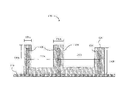
In one embodiment, as illustrated in FIG. 1, such a layer 100 having a
microbially-resistant surface can include a support substrate 110, a carbon
nanotube
layer 120 coupled to the support substrate 110, and an infiltrant material 125
infiltrated
into the carbon nanotube layer 120. Application of the infiltrant material 125
to the
carbon nanotube layer 120 can form a microbially-resistant topological
pattern. As
shown in FIG. 1, the carbon nanotube layer 120 is infiltrated with the
infiltrant material
125 to form a plurality of surface features 128, that collectively form the
topological
pattern that is microbially-resistant. It is noted that the individual
features described as
the carbon nanotube layer 120 can include a single carbon nanotube, or
multiple carbon
8
CA 02965679 2017-04-24
WO 2016/069811 PCT/US2015/057908
nanotubes that are represented by a single carbon nanotube pillar (i.e., the
carbon
nanotube layer 120) in FIG. 1.
Each surface feature 128 has a diameter, such as 130a or 130b, and a height,
such
as 140a or 140b. Additionally, a center-to-center distance, such as 150a or
150b, can be
maintained between individual surface features. Although only two variations
in
diameter, height, and distance between surface features are illustrated, a
large number of
variations in diameters, heights, and distances between surface features are
possible,
provided the resulting topological pattern is microbially-resistant as
described.
Accordingly, while there may be a high level of uniformity between diameters,
heights,
and/or center-to-center distances in some embodiments, other embodiments may
be more
non-uniform. Example ranges for surface feature diameters, heights, and center-
to-
center distances are provided as a generalized description to demonstrate
potential
topological pattern parameters, however it is to be understood that those
skilled in the art
are capable of varying pattern parameters and testing for microbial growth,
once in
possession of the present disclosure. It should be emphasized that FIG. 1 is a
simplified
drawing for purposes of illustration only and should not be interpreted to
literally define
an embodiment of the current technology.
The presently disclosed technology can be used on a variety of structures,
devices, and the like. Non-limiting examples can include various medical
devices,
electronic devices, any commonly touched surface, and the like. For example,
in one
aspect the microbially-resistant layer can be applied to a medical device,
structure,
system, etc. Such can include any surface where reduced microbial growth is
desired,
whether inserted into a biological environment, part of a device or system in
a medical
environment, a diagnostic tool, a reusable item, a surface in a medical
environment, or
the like. Non-limiting examples can include surgical implements or
instruments,
9
CA 02965679 2017-04-24
WO 2016/069811 PCT/US2015/057908
implantable devices, insertable devices, diagnostic devices, prosthetic
devices, medical
instruments, surgical or emergency room surfaces, and the like, as well as any
other
surface where microbes can grow and be spread from. Other specific non-
limiting
examples can include scalpels, scissors, drill bits, rasps, trocars, rongeurs,
graspers,
clamps, retractors, distractors, dilators, suction tips, tubes, staples and
staplers, staple
removers, needles, scopes, measurement devices, carriers and applicators,
stents, pins,
screws, plates, rods, valves, orthopedic implants, cochlear implants,
pacemakers,
catheters, sensors and monitors, bite blocks, and the like.
In another aspect, the microbially-resistant layer can be applied to an
electronic
device, systeni, or other electronically-related surface. Non-limiting
examples can
include mobile phones, laptops, keyboards, mice, computer terminals, tablets,
watches,
touch screens, game controllers, and the like.
Non-limiting examples of other devices and surfaces that may be of concern can
include doorknobs, soap dispensers, crosswalk buttons, handrails, support
rails,
countertops, food preparation and serving items, and the like.
In one embodiment the current technology can employ a carbon nanotube layer
coupled to the support substrate. As will be recognized in the art, there are
a variety of
methods to manufacture carbon nanotubes, such as arc discharge, laser
ablation, plasma
torch, chemical vapor deposition (CVD), and others. The present scope is not
limited by
the technique of preparing the carbon nanotubcs, or by the particular
technique of
infiltration. In one non-limiting example using MEMS manufacturing processes,
a mask
can be made with a detailed 2-dimensional geometry. The carbon nanotubes can
be
grown vertically extruding the 2-dimensional geometry into a 3-dimensional
carbon
nanotube forest. Thus, in one aspect, the carbon nanotube layer of the current
technology can be grown from the support substrate, either by this or another
technology,
CA 02965679 2017-04-24
WO 2016/069811 PCT/US2015/057908
with or without using a mask. In another aspect, the carbon nanotubes can be
grown or
otherwise produced on a separate substrate, removed, and subsequently
deposited on the
support substrate in a molded fashion to form the carbon nanotube layer.
The carbon nanotube layer can be formed or otherwise deposited onto the
support
substrate, and the infiltrant material can be infiltrated into the carbon
nanotube layer to
folin a topological pattern of surface features that is microbially-resistant.
The carbon
nanotube layer can be applied to the support substrate in a pattern that
assists in the
formation of the topological pattern as described, or the carbon nanotubes can
be applied
irrespective of the final topological pattern. Various infiltrant materials
can be utilized,
including, without limitation, carbon, pyrolitie carbon, carbon graphite,
silver,
aluminum, molybdenum, titanium, nickel, silicon, silicon carbide, polymers,
and
combinations thereof.
After infiltrating with the infiltrant material, the resulting layer can be
microbially-resistant, independent of chemical composition. For example, the
microbially -resistant topological pattern of surface features can be
configured to oppose
microbial or bacterial contact with the support substrate. Thus, the bacteria
can be
restricted at the termini of a group of surface features and prevented from
accessing and
adhering to the support surface to replicate and grow. Furthermore, the
surface features
themselves, or combinations thereof, can be configured or spaced so as not to
provide an
adequate growth surface for the bacterial cell. In other words, the
topological pattern of
surface features has a surface feature density that is sufficient to limit
microbial contact
with the support substrate and insufficient for the surface features
themselves to act as a
microbial growth substrate. As such, infiltrated carbon nanotube layer does
not include
an adequate surface that promotes microbial or bacterial growth.
11
CA 02965679 2017-04-24
WO 2016/069811 PCT/US2015/057908
Accordingly, the microbially-resistant topological pattern of surface features
can
be configured to reduce bacterial growth on the support substrate. In one
embodiment,
the microbially-resistant topological pattern of surface features can provide
a
bacteriostatic surface by preventing the bacteria from adhering to the surface
and
replicating. In another embodiment, the microbially-resistant topological
pattern of
surface features can provide a bactericidal surface. In one aspect, the
surface can be
bactericidal where the surface features are configured to puncture or pierce
the cell
wall/membrane of the bacterial cell. In another aspect, the surface can be
bactericidal
where the surface features are configured to tear or rupture the cell
wall/membrane of the
bacterial cell as its own mass bears down on the individual surface features.
In order to form the microbially-resistant topological pattern of surface
features,
the pattern and surface features are combined in a bacterially-resistant
manner. For
example, the pattern can provide a spacing between surface features that
prevents or
reduces access of bacterial cells to the support substrate. However, the
spacing may also
be sufficiently large so that the surface features themselves do not provide a
growth
substrate for the bacterial cell. Similarly, the surface features can have
appropriate
diameters and heights to accommodate the spacing between the surface features
in order
to restrict the bacterial cell from the support substrate and without
providing a growth
surface for the bacterial cell, as has been described. Thus, different
combinations of
densities, diameters, heights, and the like can achieve a suitable microbially-
resistant
topological pattern of surface features, which can be optimized for specific
applications
and bacterial cells.
Accordingly, the microbially-resistant topological pattern of surface features
can
have a variety of densities. In one aspect, the mierobially-resistant
topological pattern of
surface features can have a density of from 1 surface feature per iiim2 to
10,000 surface
12
CA 02965679 2017-04-24
WO 2016/069811 PCT/US2015/057908
features per 1.1m2. In another aspect, the bacterially-resistant topological
pattern of
surface features can have a density of from 25 surface features per [tm2 to
7300 surface
features per im2. In another aspect, the bacterially-resistant topological
pattern of
surface features can have a density of from 750 surface features per p.m2 to
5000 surface
features per [1111.2.
The surface features can have a variety of diameters. The diameter of the
surface
feature can be relevant for a variety of reasons. For example, if the diameter
is too small,
the surface feature can lack sufficient stiffness to support a bacterial cell.
Thus, the
surface feature can be displaced or bent in such a way as to allow the
bacterial cell access
to the support substrate for adhesion, growth, and replication. However, if
the diameter
is too large, the surface features can begin to abut one another, or they can
be sufficiently
large themselves, to provide a growth surface for the bacteria. Further,
different
infiltrant materials can impart different structural characteristics, and as
such, infiltration
to different diameters may be useful for different materials. In one general
aspect, the
surface features can have a diameter of from 10 nm to 1000 nm. In another
general
aspect, the surface features can have a diameter of from 50 nm to 500 nm. In
another
general aspect, the surface features can have a diameter of from 100 nm to 200
nm.
The surface features can also have a variety of heights. The relevance of a
specified height parallels that of the description of diameter to some extent.
The taller a
surface feature, the more it will bend, thus allowing access to the support
substrate by the
microorganism. Thus, in one aspect, the surface features can have a height of
about 1
diameter of a bacterial cell. While bacteria can have a variety of diameters,
surface
features can be specifically designed for specific sized or specific ranges of
bacteria.
Additionally, many bacteria have a diameter ranging from 0.21,tm to 2 pm, and
as such,
13
CA 02965679 2017-04-24
WO 2016/069811 PCT/US2015/057908
in some aspects the heights of surface features can range from 0.2, 0.5, 1 or
2 um to 10,
100, or 1000 um.
However, as previously described, at any given diameter or height, the spacing
of
the surface features can be still be taken into account. In one aspect, a
center-to-center
distance can be maintained between individual surface features of from 200 nm
to 800
nm. In another aspect, a center-to-center distance can be maintained between
individual
surface features of from 200 nm to 600 nm. In another aspect, a center-to-
center distance
can be maintained between individual surface features of from 300 nm to 500
nm.
Because the configuration of the surface topography can become microbially-
resistant at various patterns, spacings, and diameters/heights of surface
features, it will be
recognized in the art, once in possession of the present disclosure, that the
carbon
nanotube layer can be replaced by a variety of other surfaces. For example, a
surface can
be molded to have the above-specified configuration, thus rendering the
surface
microbially-resistant. Further, such a surface can be etched to achieve an
equivalent
configuration. Further still, such a surface can be deposited via CVD or
physical vapor
deposition (PVD) methods. Some of these surfaces can also be infiltrated to
achieve the
desired configuration while others can be configured without infiltration.
Thus, any
surface having the specified configuration for the microbially-resistant
topological
pattern of surface features is considered to be within the scope of the
current technology,
whether it has a carbon nanotube layer or not.
In another embodiment, a method is described for reducing microbial growth on
a
surface. The method can include depositing a carbon nanotube layer on a
support
substrate and infiltrating the carbon nanotube layer with an infiltrant
material. This can
form a microbially-resistant topological pattern of surface features.
14
CA 02965679 2017-04-24
WO 2016/069811 PCT/US2015/057908
As previously described, depositing a carbon nanotube layer can be performed
using a variety of methods known in the art. In one aspect, the carbon
nanotube layer
can be grown on the support surface. In another aspect, the carbon nanotube
layer can be
deposited on the surface via at least one of CVD or PVD. In another aspect,
the carbon
-- nanotubes can be grown or deposited on a separate substrate and transferred
or applied to
the support substrate.
Suitable types of support substrates can include any type of useful material
on
which a microbially-resistant layer can be formed. In one aspect, for example,
the
support substrate can include various metals, metal alloys, polymers,
ceramics,
semiconductors, and the like, including combinations thereof. Non-limiting
examples
can include iron, steel, stainless steel, nickel, aluminum, titanium, brass,
bronze, zinc,
and the like, including combinations thereof. Other non-limiting examples can
include
polyethylenes, polyvinyl chlorides, polyethylenes, polypropylenes,
polystyrenes,
polyamides, polyimides, acrylonitrile butadiene styrenes, polycarbonates,
polyurethanes,
-- polyetheretherketones, polyetherimides, polymethyl methacrylates,
polytetrafluoroethylenes, urea-formaldehydes, furans, silicones, and the like,
including
combinations thereof. Yet other non-limiting examples can include silicon,
quartz, glass,
and the like, including combinations thereof.
Examples
Example 1 ¨ Infiltrated Carbon Nanotubes
Carbon nanotubes were grown at 750 C using ethylene gas as the carbon source
at a flow rate of about 146 seem. Iron layers 2-10 nm thick were used as a
catalyst for
nanotube growth. The samples tested for biofilm growth were grown using a 7 nm
-- catalyst layer. Nanotube density was controlled by the thickness of the
iron catalyst
CA 02965679 2017-04-24
WO 2016/069811 PCT/US2015/057908
layer deposited before growth. The carbon nanotubes were infiltrated using
ethylene gas
as a carbon source (flow rate of about 214 sccm), at 900 C, for 1-60 minutes
to produce
carbon infiltrated carbon nanotubes (CI-CNTs).
FIG. 2 shows an image of a medium (30-minute) infiltration sample from the
top.
This image illustrates surface features that are about 100-200 nm in diameter,
and are
spaced roughly 300-500 nm apart.
FIG. 3 shows an image of a low (3-minute) infiltration sample from the top. In
this case, the pillars are about 20-50 nm in diameter.
FIG. 4 shows a high (60-minute) infiltration sample from the top. In this
case,
the carbon nanotube layer has completely filled in, leaving abutting spherical
protrusions
from the surface instead of spaced surface features.
FIG. 5 shows a sample carbon nanotube forest from the side, illustrating that
the
infiltration material coats the whole length of the nanotubes, leaving behind
voids (or
pores) in the material.
Example 2 ¨ Microbially Resistance of Surfaces
MRSA biofilm testing was performed on CI-CNT surfaces to determine bacterial
resistance. Three CI-CNT samples and controls were prepared at different
infiltration
levels: low, medium, and high, as described in Example 1 above. Each of the
test
samples was inoculated with MRSA bacteria, whereas the control samples were
not.
Subsequently, each of the samples and controls were put into an environment
that would
allow MRSA bacteria to flourish and create biofilms for 48 hours. Typically,
biofilms are
generated like those illustrated in FIG. 6. However, as can be seen in FIG. 7,
there is
little to no difference between test samples and control samples, despite the
test samples
being inoculated with MRSA bacteria and provided with an optimal growth
environment
16
CA 02965679 2017-04-24
WO 2016/069811 PCT/US2015/057908
for 48 hours. Thus, while there are bacterial cells on the CI-CNT surfaces,
they did not
replicate as anticipated under the growth conditions to produce typical
biofilms, as
illustrated in FIG. 6. This would indicate that the CI-CNT surfaces resist
bacterial
growth and replication.
An additional study was performed similar to the previous test with the
exception
that 24 samples were tested at one time. Each of the samples was placed in the
same
chamber for a 48-hour incubation period. Representative SEM images are
illustrated by
FIG. 8. There are morphological differences between the various images, but
this is not
uncommon for biofilms. The medium infiltration resisted the biofilm better
than both the
low and high infiltration samples. Further, based on the infiltration
parameters described
in Example 1, it was observed that a highly effective surface feature
configuration can be
obtained by infiltrating for about 16 minutes at 950 C.
Example 3 ¨ Growing CI-CNTs on Stainless Steel
Iron is a catalyst for CNT growth. Accordingly, this study explored whether
the
iron present in stainless steel (SS) can be used as a catalyst for CNT growth.
As can be
seen in FIG. 9, CNTs can be grown directly on the SS surface without an
external
catalyst. This can dramatically simplify the manufacturing process. Also,
because the
catalyst is inside the substrate, the adhesion strength can be improved. This
can allow for
coating SS medical implants or tools with CNTs to gain the benefit of their
antibacterial
properties.
Though a variety of methods can be used, the current SS samples were etched in
high concentration HCI for 15 minutes. The samples were then transferred into
a furnace
for growth and infiltration. This etching process can partially remove the
chromium-
oxide layer on the SS and allow for iron to be used as the catalyst during CNT
growth.
17
CA 02965679 2017-04-24
WO 2016/069811 PCT/US2015/057908
The SS samples were analyzed by SEM imaging and scratch tests. The top
surfaces were SEM imaged to see if they matched silicon substrate surfaces
visually. As
shown in FIG. 9, SS samples do match the silicon substrates having medium
infiltration
levels, but the samples did require a longer infiltration time. Scratch
testing was
performed by using sharp tweezers to scratch on the surface (FIG. 10).
Generally, the
adhesion for CI-CNTs on SS is polarized, such that they either adhere very
well or they
flake off with a minimal contact.
As illustrated in FIG. 11, a 15-second growth on SS can result in about a 4 pm
growth height. Growth density and characteristics are generally similar to the
typical
silicon samples.
Example 4 ¨ Growing CI-CNTS on Various Substrate Configurations
One of the unique features of CI-CNTs is that they "grow," which means that
they have the potential to be coated onto a variety of surface geometries.
Accordingly,
this study looked at the characteristics of CI-CNTs grown on various surface
geometries.
First, 3 mm diameter rods were coated with CI-CNTs. It was discovered that
convex
substrates can have problems with cracking (FIG. 12).
In order to evaluate the cause for this cracking phenomenon, iron thickness,
CNT
height, infiltration level, and cooling time after growth were measured. The
results
indicated that iron thickness and CNT height were the primary variables that
affected
cracking. Increasing iron thickness decreased the area of cracks. Increasing
the CI-CNT
height increased the area of cracks (FIG. 13). Thus, optimization of these
variables can
be used to minimize, and eventually eliminate, CI-CNT cracks on concave
surfaces.
Concave substrates were also evaluated. Specifically, two variables were
tested:
radius of curvature and CI-CNT height. Quartz tubes were cut along the axis,
and CI-
18
CA 02965679 2017-04-24
WO 2016/069811
PCT/US2015/057908
CNTs were grown using the same methods as a silicon wafer substrate (FIGs. 14A-
B).
After the growth and infiltration, each tube was broken in half to SEM image
the inside
cross-section. These SEM images exposed defects in the growths such as CNT
curving
and inside crevices (FIG. 15) that confirm the importance of coordinating
inner diameter
(ID) and CI-CNT height. Examples of the SEM results can be seen in F1Gs. 16A-
16D.
Overall, long CI-CNT growths combined better with large IDs (3-4mm) than small
IDs
(1-2 mm). However, short CI-CNT growths combine well with all IDs tested. One
potential drawback to the short CI-CNT growths is that they can be quite
fragile. This
can result partially because the CNTs do not adhere to the quartz tubing.
However, this
will not be an issue when they are adhered to a substrate such as stainless
steel.
While the forgoing examples are illustrative of the principles of the present
invention in one or more particular applications, it will be apparent to those
of ordinary
skill in the art that numerous modifications in form, usage and details of
implementation
can be made without the exercise of inventive faculty, and without departing
from the
principles and concepts of the invention. Accordingly, it is not intended that
the
invention be limited, except as by any claims associated with this or related
applications.
19