Note : Les descriptions sont présentées dans la langue officielle dans laquelle elles ont été soumises.
Docket No. 091443-00066
LOW-COST DRIVER CIRCUIT WITH IMPROVED POWER FACTOR
Technical Field
[0001] The present disclosure relates generally to a driver circuit for
powering a load, and
more particularly to a driver circuit having an improved power factor (PF)
that includes a
feedback circuit for maintaining a charge on a voltage bus filter.
Background
[0002] Light emitting diode (LED) based lighting systems may offer several
energy and
reliability advantages over other types of lighting systems such as, for
example,
incandescent or fluorescent lighting. Thus, LED based lighting systems may be
an
attractive candidate to replace other existing lighting technologies.
[0003] Historically, incandescent light bulbs have had a nearly perfect power
factor (PF).
In other words, incandescent bulbs typically have a PF of about 1. Those
skilled in the art
will readily appreciate that electrical devices having a relatively low PF
require additional
power from the utility, which is also referred to as grid power. Accordingly,
high power
factor solutions are desirable for LED based lighting system. In particular,
it may be
especially desirable for an LED based lighting fixture to have a PF of at
least 0.7 in order
to obtain specific types of energy certifications promulgated by the United
States
government (e.g., the ENERGY STAR certification). This is because some
potential
consumers of lighting products may make purchasing decisions based on whether
or not an
LED lighting fixture has obtained one or more specific types of energy
certifications.
Moreover, those skilled in the art will also appreciate there is also a
continuing need in the
art for a relatively low-cost, reliable driver for an LED lighting fixture as
well.
Summary
[0004] In one embodiment, a driver circuit for powering a load is disclosed.
The driver
circuit includes an input for receiving for connection to a source of AC
power, and a
rectifier for converting the AC power from the input into DC power. The driver
circuit
also include a voltage bus filter, a high-frequency oscillator for generating
a high-
frequency AC signal, a resonant driver, a feedback circuit, and a high-
frequency DC
rectifier. The voltage bus filter smoothens the DC power from the rectifier,
and includes at
1
Date Recue/Date Received 2021-01-21
least one capacitor. The resonant driver is in electrical communication with
the high-
frequency oscillator, and limits a current of the high-frequency AC signal and
produces a
limited output voltage based on the high-frequency AC signal. The feedback
circuit is in
electrical communication with the resonant driver and the voltage bus filter,
and maintains
a charge on the capacitor of the voltage bus filter. The high-frequency DC
rectifier is in
electrical communication with the resonant driver and rectifies the limited
output voltage
into a DC output voltage including a substantially constant current for
powering the load.
A blocking capacitor is provided in electrical communication with the
rectifier, the voltage
bus filter, and the high-frequency DC rectifier, the blocking capacitor
located between the
rectifier and the high-frequency DC rectifier, wherein the blocking capacitor
allows for the
high-frequency AC signal generated by the high-frequency oscillator to flow to
the high-
frequency DC rectifier and blocks the DC output voltage generated by the high-
frequency
DC rectifier from flowing back to the rectifier.
[0005] In another embodiment, a driver circuit for powering at least one light
emitting
diode (LED) in a non-dimming application is disclosed. The driver circuit
includes an
input for receiving for connection to a source of AC power, and a rectifier
for converting
the AC power from the input into DC power. The driver circuit also include a
voltage bus
filter, a high-frequency oscillator for generating a high-frequency AC signal,
a resonant
driver, a feedback circuit, and a high-frequency DC rectifier. The voltage bus
filter
smoothens the DC power from the rectifier, and includes at least one
capacitor. The
resonant driver is in electrical communication with the high-frequency
oscillator, and limits
a current of the high-frequency AC signal and produces a limited output
voltage based on
the high-frequency AC signal. The feedback circuit is in electrical
communication with the
resonant driver and the voltage bus filter. The feedback circuit comprises a
capacitor that
acts as acts as a charge pump that maintains a charge on the at least one
capacitor of the
voltage bus filter. The high-frequency DC rectifier is in electrical
communication with the
resonant driver and rectifies the limited output voltage into a DC output
voltage including a
substantially constant current for powering the LED. A blocking capacitor is
provided in
electrical communication with the rectifier, the voltage bus filter, and the
high-frequency
DC rectifier, the blocking capacitor located between the rectifier and the
high-frequency
DC rectifier, wherein the blocking capacitor allows for the high-frequency AC
signal
generated by the high-frequency oscillator to flow to the high-frequency DC
rectifier and
- 2 -
Date Recue/Date Received 2021-01-21
blocks the DC output voltage generated by the high-frequency DC rectifier from
flowing
back to the rectifier.
Brief Description of the Drawings
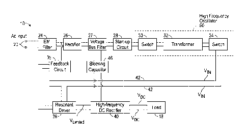
[0006] FIG. 1 is an exemplary block diagram of a circuit with an improved
power factor
(PF) for providing DC current to a load;
[0007] FIG. 2 is an exemplary circuit diagram of the circuit shown in FIG. 1,
where a
rectifier includes fast recovery diodes;
[0008] FIG. 3 is an illustration of an exemplary AC waveform at inputs of the
circuit
shown in FIGS. 1 and 2, as well as a rectified input voltage measured at a
voltage bus filter of
the circuit;
[0009] FIG. 4 is an illustration of a resonant curve and an operating point of
the resonant
driver shown in FIGS. 1 and 2;
[0010] FIG. 5 is an alternative embodiment of the circuit diagram shown in
FIG. 2, where
the rectifier does not include fast recovery diodes; and
[0011] FIG. 6 is another embodiment of the circuit diagram shown in FIG. 5,
where the
location of a blocking capacitor is modified.
Detailed Description
[0012] The following detailed description will illustrate the general
principles of the
invention, examples of which are additionally illustrated in the accompanying
drawings. In
the drawings, like reference numbers indicate identical or functionally
similar elements.
[0013] FIG. 1 is an exemplary block diagram of a circuit 10 for providing DC
current to
a load 18. The driver circuit 10 may include a pair of power input lines 20
for connection
to a source (not shown) of AC power such as, for example, main power lines at
a nominal
120 volts AC. The driver circuit 10 may also include a resistor R1 (shown in
FIG. 2), an
electromagnetic interference (EMI) filter 24, a rectifier 26, a voltage bus
filter 27, a start-up
circuit 28, a switch 30, a transformer 32, a switch 34, a feedback circuit 35,
a resonant
driver circuit 36, a high-frequency DC rectifier 40, and a blocking capacitor
46. As
- 3 -
Date Recue/Date Received 2021-01-21
explained in greater detail below, the circuit 10 provides substantially
constant DC current
to the load 18, while maintaining a relatively high power factor (PF). In one
embodiment,
the circuit 10 may include a PF of at least 0.7.
[0014] Referring to FIGS. 1-2, the input lines 20 of the driver circuit 10 may
be in
electrical communication with the EMI filter 24. In one non-limiting
embodiment the EMI
filter 24 may include an inductor Li and capacitors Cl and C2 (shown in FIG.
2). The
rectifier 26 may be in electrical communication with the EMI filter 24, and is
configured to
convert incoming AC power from the EMI filter 24 to a pulsing DC power. In the
embodiment as shown in FIG. 2, the rectifier 26 is a high-frequency bridge
rectifier
including four fast recovery diodes D1, D2, D3, D4. In one embodiment, the
fast recovery
diodes Dl-D4 may have a response time of less than about 150 ns, however it is
to be
understood that this parameter is merely exemplary in nature, and that other
types of fast
recovery diodes may be used as well.
[0015] The output of the rectifier 26 may be in electrical communication with
the voltage
bus filter 27. In the exemplary embodiment as shown in FIG. 2, the voltage bus
filter 27
may include a capacitor C3. Those of ordinary skill in the art will readily
appreciate that
the capacitor C3 may be an electrolytic capacitor that acts as a smoothing
capacitor.
Specifically, the capacitor C3 may be used to smoothen or reduce the amount of
ripple in
the DC power provided by the rectifier 26 such that relatively steady DC power
may be
provided to the remaining components within the circuit 10 (i.e., the start-up
circuit 28, the
switch 30, the transformer 32, the switch 34, the resonant driver circuit 36,
and the high-
frequency DC rectifier 40). As explained in greater detail below, the feedback
circuit 35
may be used to create a charge on the capacitor C3. Maintaining a charge on
the capacitor
C3 further smoothens the DC power provided by the rectifier 26, which in turns
improves
the PF of the circuit 10.
[0016] Continuing to refer to both FIGS. 1 and 2, the voltage bus filter 27
may be in
electrical communication with the start-up circuit 28. The start-up circuit 28
may include
resistors R2 and R3, diode D6, diac D7, and capacitor C6. The diac D7 is a
diode that
conducts current only after a breakover voltage, VB0, has been reached. During
initial
start-up of the circuit 10, the capacitor C6 may be charged until the diac D7
reaches the
breakover voltage VB0. Once the breakover voltage is reached, the diac D7 may
start to
- 4 -
Date Recue/Date Received 2021-01-21
conduct current. Specifically, the diac D7 may be connected to and sends
current to the
switch 30. Once the diac D7 attains the breakover voltage VB0, the diode D6
may be used
to discharge the capacitor C6 and to prevent the diac D7 from firing again.
[0017] As seen in FIG. 2, the circuit 10 may include a lower switch 30
(labelled Q2) and
an upper switch 34 (labelled Q1) connected in a cascade arrangement. Referring
to both
FIGS. 1 and 2, the resistor R3 may be used to provide bias to the lower
switching element
Q2. In the embodiment as shown in FIG. 2, the switching element Q2 is a
bipolar junction
transistor (BJT). Although a BJT may be a relatively economical and cost-
effective
component used for switching, those skilled in the art will appreciate that
other types of
switching elements may be used as well. A diode D10 may be provided to limit
negative
voltage between a base B and an emitter E of the switching element Q2, which
in turn
increases efficiency.
[0018] The switch 30 may be connected to the transformer 32. As seen in FIG.
2, in an
embodiment the transformer 32 includes three windings, T1A, T1B, and TIC. The
winding TlA may include an opposite polarity when compared to the winding T1B.
This
ensures that if the switching element Q2 is turned on, another switching
element Q1 will
not turn on at the same time.
[0019] Referring to FIGS. 1-2, both the switches 30, 32, diodes D9, D10,
resistors R5 and
R6, and the transformer 32 define a high-frequency oscillator 50. The high-
frequency
oscillator 50 generates a high-frequency AC signal VIN (shown in FIG. 1). In
one
embodiment, the high-frequency AC signal YIN may be an AC signal having a
frequency of
at least about 40 kilohertz (kHz). An output 42 (shown in FIG. 1) of the high-
frequency
oscillator 50 may be in electrical communication with the resonant driver
circuit 36.
[0020] Referring to FIG. 2, the upper switching element Q1 may also be a BJT.
A diode
D9 may be provided to limit negative voltage between a base B and an emitter E
of the
upper switching element Ql, which in turn increases efficiency. The switch 34
may be
used to electrically connect the high-frequency oscillator 50 to the resonant
drive circuit 36.
In the embodiment as shown in FIG. 2, the resonant drive circuit 36 may
include a
capacitor C7 connected in series with the winding T1C of the transformer 32.
The resonant
drive circuit 36 may also include an inductor L2. The resonant drive circuit
36 may be
- 5 -
Date Recue/Date Received 2021-01-21
used to limit the current of the high-frequency AC signal YIN received from
the high-
frequency oscillator 50. The resonant drive circuit 36 also produces a limited
output
voltage VLIMITED (shown in FIG. 1) based on the high-frequency AC signal YIN-
10021] The resonant driver circuit 36 may be in electrical communication with
the high-
frequency DC rectifier 40. The limited output voltage VLIMITED created by the
resonant
driver 36 may be sent to the high-frequency DC rectifier 40, and is rectified
into a DC
output voltage VDc (shown in FIG. 1). The DC output voltage VDc includes a
substantially
constant current that is supplied to the load 18. In the embodiment as shown
in FIG. 2, the
high-frequency DC rectifier 40 is a full wave rectifier including four diodes
D11-D14 and a
filter capacitor C8. The full-wave rectifier may be connected in parallel with
the filter
capacitor C8. In one embodiment, the diodes D11-D14 may be low voltage diodes.
It is to
be understood that the full wave rectifier 40 doubles the frequency of limited
output
voltage VLIMITED from the resonant circuit 36, therefore the filter capacitor
C8 may be
relatively small in size. For example, in one embodiment, the filter capacitor
C8 may be
less than one microfarad.
[0022] Continuing to refer to FIGS. 1-2, the blocking capacitor 46 may include
a
capacitor C4. The capacitor C4 is in electrical communication with the
rectifier 26, the
voltage bus filter 27, and the high-frequency DC rectifier 40. The capacitor
C4 may be
used for impedance matching and for blocking DC current. Specifically, the
capacitor C4
allows for the high-frequency AC signal VIN (shown in FIG. 1) generated by the
high-
frequency oscillator to flow to the high-frequency DC rectifier 40. The
capacitor C4 also
blocks the DC output voltage VDC generated by the high-frequency DC rectifier
40 located
on the right side of the circuit 10 from flowing back to the rectifier 26. In
the embodiment
as shown in FIG. 2, the blocking capacitor C4 is located between the rectifier
26 and the
high-frequency DC rectifier 40. However, in an alternative embodiment, the
blocking
capacitor 46 may be connected to the emitter E of the switch 30.
[0023] The feedback circuit 35 may be connected to the circuit 10 between the
EMI filter
24 and the rectifier 26. The feedback circuit 35 may also be connected to the
high-
frequency DC rectifier 40. The feedback circuit 35 includes a capacitor C5,
which acts as a
charge pump that maintains a charge on the capacitor C3 of the voltage bus
filter 27, which
in turn increases the PF of the circuit 10. Turning now to FIG. 3, an
exemplary illustration
- 6 -
Date Recue/Date Received 2021-01-21
of an AC waveform A received by the inputs 20 of the circuit 10 is shown. FIG.
3 also
illustrates a rectified input voltage VREc of the circuit 10, which is
measured after the
rectifier 24 at the capacitor C3 of the voltage bus filter 27. The rectified
input voltage VREC
is based on the AC waveform received by the inputs 20 of the circuit 10.
[0024] Referring to both FIGS. 2 and 3, the rectified input voltage VREc
includes ripples
R. It is to be understood that the amplitude of the ripples R of the rectified
input voltage
VREC may be reduced due to the feedback circuit 35 maintaining a charge on the
capacitor
C3 of the voltage bus filter 27. In other words, maintaining a charge on the
capacitor C3
will in turn further smoothen or reduce the amount of ripple in the rectified
input voltage
VREc through each half cycle of the AC waveform A at the inputs 20 of the
circuit 10 (the
half cycles of the AC waveform A are labelled in FIG. 3). Moreover,
maintaining a charge
on the capacitor C3 will also result in increased conduction time of the
current at the
inputs 20 of the circuit 10. Accordingly, the feedback circuit 35 may improve
the overall
PF of the circuit 10. For example, in one embodiment, the overall PF of the
circuit 10 may
be at least 0.7.
[0025] Turning back to FIG. 2, in one embodiment, the load 18 may be one or
more light
emitting diodes (LEDs). For example, in embodiments as shown in FIGS. 2-6 the
circuit
may include a pair of output terminals 44 that connect to a LED (not shown).
In the
embodiments as described and illustrated in the figures, the driver circuit 10
is used in a
non-dimmable LED application. Although an LED is described, it is to be
understood that
the load 18 may be any type of device that requires a substantially constant
current during
operation. For example, in an alternative embodiment, the load 18 may be a
heating
element.
[0026] FIG. 4 is an illustration of an exemplary resonance curve of the
resonant drive
circuit 36 shown in FIG. 2. The resonance curve may include an operating point
0 and a
resonant critical frequency fc,. The critical frequency f0 is located at a
peak of the
resonance curve, and the operating point 0 is located to the left of the
critical frequency f..
Referring to both FIGS. 2 and 4, increasing the capacitance of the capacitor
C7 or the
inductance of the inductor L2 of the resonant driver 36 may shift the critical
frequency f, to
the left, and decrease the capacitance of the capacitor C7 or the inductance
of the inductor
L2 may shift the critical frequency f0 to the right. The frequency of
oscillation of the
- 7 -
Date Recue/Date Received 2021-01-21
resonance curve may be determined by winding T1C of the transformer 32,
resistors R5
and R6, the upper switching element Ql, and the lower switching element Q2. In
particular, the frequency of oscillation of the resonance curve may be based
upon a number
of the turns of the winding T1C of the transformer 32, as well as the storage
times of the
upper switching element Q1 and the lower switching element Q2.
[0027] The inductance of the inductor L2 as well as the capacitance of the
capacitors C4
and C7 may be key factors in maintaining acceptable line regulation of the
circuit 10.
Specifically, as line voltage increases a frequency of operation of the
circuit 10 decreases.
Moreover, the impendence of the inductor L2 may decrease as the frequency of
operation
decreases, thereby causing an increase in current that is delivered to the
load 18 (FIG. 1).
Thus, the inductance of the inductor L2 as well as the capacitance of the
capacitors C7 and
the capacitor C4 may be selected such that an overall gain of the circuit 10
decreases as the
frequency of operation decreases. This in turn may substantially decreases or
minimize
any increase in current that is delivered to the load 18 as the line voltage
increases.
[0028] FIG. 5 is an illustration of an alternative circuit 100. The circuit
100 includes
similar components as the circuit 10 shown in FIG. 2. However, the circuit 100
also
includes two additional diodes D15 and D16 that are located after the
rectifier 26. In the
embodiment as shown in FIG. 5, the diodes D15, D16 are fast recovery diodes.
Diode D15
may be located between the rectifier 26 and diode D16. Diode D16 may be
located
between diode D15 and the high-frequency DC rectifier 40. Since the circuit
100 includes
fast recovery diodes D15 and D15, the diodes D1-D4 of the rectifier 26 do not
need to be
fast recovery diodes as well. In other words, the recitifer 26 is a standard
bridge rectifier.
Accordingly, the circuit 100 shown in FIG. 5 may result in a reduced number of
fast
recovery diodes when compared to the circuit 10 shown in FIG. 10.
[0029] FIG. 6 is yet another embodiment of a circuit 200. The circuit 200
includes
similar components as the circuit 100 shown in FIG. 5. However, the location
of the
blocking capacitor C4 has been modified. Specifically, the blocking capacitor
C4 is now
connected between diode D15 and the resonant driver circuit 36. Also, the
location of the
capacitor C5 of the feedback circuit 35 has also been modified. Specifically,
the capacitor
C5 is now located in parallel with the diode D16. However, capacitor C5 still
acts as a
charge pump to maintain the chage on the capacitor C3 of the voltage bus
filter 27. An
- 8 -
Date Recue/Date Received 2021-01-21
additional capacitor C11 has been added to the circuit 200, and is in parallel
with the
capacitor C3 of the voltage bus filter 27. The capacitor C11 acts as a
divider.
[0030] The disclosed circuit as illustrated in FIGS. 1-6 and described above
provides a
relatively low-cost and efficient approach for driving a load, while at the
same time
providing a relatively high PF (i.e., above 0.7). In particular, the disclosed
circuit provides
a relatively high PF without the need for active circuitry, which adds cost
and complexity
to an LED lighting fixture. Furthermore, the disclosed circuit also provides a
relatively
low-cost and efficient approach for delivering substantially constant current
to a load as
well. Those skilled in the art will readily appreciate that the disclosed
circuit results in
fewer components and a simpler design when compared to some types of LED
drivers
currently available on the market today.
[0031] While the forms of apparatus and methods herein described constitute
preferred
embodiments of this invention, it is to be understood that the invention is
not limited to
these precise forms of apparatus and methods, and the changes may be made
therein
without departing from the scope of the invention.
- 9 -
Date Recue/Date Received 2021-01-21