Note : Les descriptions sont présentées dans la langue officielle dans laquelle elles ont été soumises.
CA 06 9647 2017--132
WO 2016/089245 PCT/RU2014/000913
A modified RF power combiner
The present invention relates to RF power combiners or RF
power splitters.
RF power combiners are devices used in radio technology when
there is a requirement of combining RF (radio frequency)
power or RF signals. RF power combiners receive a plurality
of RF inputs and transform the impedance of the received RF
inputs to impedance of a single output. RF power splitters,
also known as RF power dividers, are devices used in radio
technology when there is a requirement of splitting RF power
or RF signals. RF power splitters receive a single RF input
and transform the impedance of the received RF input to
impedance of a plurality of RF outputs. Thus, RF power
combiners and RF splitters are basically the same RF device
and include a matching circuit. The matching circuit can be
used to combine or to split RF power, the only difference
being that RF power is applied to one port and extracted from
other in the case of the RF splitter, and for the RF
combiner, RF power is applied in the opposite direction.
The RF power combiners or the RF power splitters in the
present disclosure mean one and the same thing which has been
hereinafter referred to as the RF power combiner. The RF
power combiner known in the art of radio technology have
linear orientation thereby placing the RF power input and RF
power output in a linear alignment on different sides of the
RF power combiner. When such a conventional RF power combiner
is used in assembly of a RF tract and placed in a
standardized modular system, for example a 19-inch rack, a
requirement to have the RF connectors transmitting the RF
output or the RF input at the same side of such a
standardized module is generated. In order to fulfill this
requirement additional waveguide bends are used, for example
E-bends or H-bends if the RF system is based on a rectangular
waveguide architecture, or coaxial 'elbows' if the RF system
CA 06 9647 2017-06-02
WO 2016/089245 PCT/RU2014/000913
2
operates with coaxial lines. This results in bigger overall
dimensions and higher costs of the RF system as the assembly
of such RF system or RF tract involves multiple components
i.e. at least the power combiner and the additional waveguide
bends.
Moreover in most cases, physical contacts, e.g. waveguide
flanges, are also required to establish and maintain
connection between the additional waveguide bends and the RF
output or the RF input in the RF tract. The physical contacts
need to be protected against disruption or dislocation in
order to ensure proper functioning of the RF power combiner
and thus to ensure that the performance of the entire RF
system is not jeopardized. Moreover, assembling such a RF
tract or RF system with multiple RF devices i.e. the
conventional RF power combiner, additional waveguide bends,
waveguide flanges, etc is complex and cumbersome and thus
requires expertise and experience.
Thus the object of the present technique is to provide a
modified RF combiner which is compact, easy to integrate into
a RF tract, and which at least partially obviates
possibilities of disruption of connection between the
additional waveguide bends and the RF output or the RF input
of the RF power combiner in the RF tract.
The above objects are achieved by a modified RF power
combiner according to claim 1 of the present technique.
Advantageous embodiments of the present technique are
provided in dependent claims. Features of claim 1 may be
combined with features of dependent claims, and features of
dependent claims can be combined together.
According to an aspect of the present technique, a modified
RF power combiner is presented. The modified RF power
combiner includes a matching circuit, a plurality of first RF
ports, exactly one second RF port and a casing. The matching
circuit is arranged inside the casing. The plurality of first
CA 069647 2017--132
WO 2016/089245 PCT/RU2014/000913
3
RF ports and the second RF port are arranged at a first side
of the casing. In the modified RF power combiner, the second
RF port is connected in series with the matching circuit and
each of the plurality of the first RF ports. As a result, the
modified RF power combiner is compact when introduced in a RF
tract or a RF system or any standardized module as
requirement of having additional waveguide bends is at least
partially reduced. Moreover, since the requirements of
additional waveguide bends and physical contacts such as
waveguide flanges is obviated, disruption of connection
between the additional waveguide bends and the RF output or
the RF input of the RF power combiner in the RF tract is
obviated. Furthermore, integration of the modified RF power
combiner into a RF tract or standardized module is easier and
hassle free.
In an embodiment of the modified RF power combiner, each of
the first RF ports is connected via an inner conductor to the
matching circuit. This ensures that RF power can be
conveniently provided to the matching circuit arranged inside
the casing through the first RF ports when the modified RF
power combiner is functioning to combine RF power and without
requiring disassembly of or opening of the casing.
Alternatively, this also ensures that RF power can be
conveniently received from the matching circuit arranged
inside the casing through the first RF ports when the
modified RF power combiner is functioning to split RF power
and without requiring disassembly of or opening of the
casing. The first RF ports are connected to the matching
circuit in parallel.
In another embodiment of the modified RF power combiner, each
of the inner conductors is arranged inside the casing. Thus
the casing protects the inner conductors and further ensures
that any possibility of disruption of connection between the
first RF ports and the matching circuit, when the modified RF
power combiner is being integrated into a RF tract or being
CA 02969647 2017-06-02
WO 2016/089245 PCT/RU2014/000913
4
stored or transported or while in operation as part of a RF
tract, is at least partially obviated.
In another embodiment of the modified RF power combiner, the
second RF port is connected via a single transmission line to
the matching circuit. This ensures that RF power can be
conveniently received from the matching circuit arranged
inside the casing through the second RF port when the
modified RF power combiner is functioning to combine RF power
and without requiring disassembly of or opening of the
casing. Alternatively, this also ensures that RF power can be
conveniently provided to the matching circuit arranged inside
the casing through the second RF port when the modified RF
power combiner is functioning to split RF power and without
requiring disassembly of or opening of the casing.
In another embodiment of the modified RF power combiner, the
single transmission line is arranged inside the casing. Thus
the casing protects the single transmission line and further
ensures that any possibility of disruption of connection
between the second RF port and the matching circuit, when the
modified RF power combiner is being integrated into a RF
tract or being stored or transported or while in operation as
part of a RF tract, is at least partially obviated.
In another embodiment of the modified RF power combiner, the
single transmission line forms a 180 degree turn in between
the matching circuit and the second RF port. This provides a
simple way of arranging the matching circuit and the single
transmission line within the casing and relative to the
second RF port.
In another embodiment of the modified RF power combiner, the
casing is cuboidal in shape. The first side of the casing is
one of the faces of the cuboid. Such a casing is easy to
fabricate and can be fabricated in a size that is compatible
with standardized frames or enclosures for mounting multiple
equipment modules.
CA 069647 2017--132
WO 2016/089245 PCT/RU2014/000913
In another embodiment of the modified RF power combiner, the
casing is adapted to be mountable inside a 19-inch rack. Such
19-inch racks or 19-inch cabinets are used in various RF
5 tracts or systems and thus the modified RF power combiner is
physically compatible to be integrated in such RF tracts or
systems.
In another embodiment of the modified RF power combiner, the
casing includes a mounting means for mounting the modified RF
power combiner inside a 19-inch rack. Thus requirement of
additional means for mounting or complicated contraptions for
mounting the modified RF power combiner inside a 19-inch rack
is at least partially obviated.
In another embodiment of the modified RF power combiner, the
mounting means is a sliding means and wherein the modified RF
power combiner is mountable inside a 19-inch rack by
slidingly engaging the sliding means with rails of the 19-
inch rack. This at least partially obviates requirement of
attaching and/or detaching the modified RF power combiner and
the 19-inch rack. Moreover, the modified RF power combiner
can be easily dismounted from the 19-inch rack which may be
required for inspection or maintenance of the modified RF
power combiner or the 19-inch rack or any other components
mounted on the 19-inch rack.
In another embodiment of the modified RF power combiner, the
mounting means is a fastening means for fixedly mounting the
modified RF power combiner inside a 19-inch rack. Thus, when
mounted inside the 19-inch rack the modified RF power
combiner stays in place and does not dislocate due to
physical disturbances of the 19-inch rack or the
surroundings.
In another embodiment of the modified RF power combiner, the
plurality of the first ports and the second port are embedded
in a wall of the casing on the first side of the casing. Thus
CA 06 9647 2017--132
WO 2016/089245
PCT/RU2014/000913
6
additional requirement of affixing the first ports and the
second port on the first side of the casing are at least
partially obviated.
In another embodiment of the modified RF power combiner, the
wall of the casing, along with the plurality of the first
ports and the second port embedded in the wall, completely
encloses a volume. The matching circuit is positioned in the
volume. Thus the matching circuit and its connections to the
first and the second ports are protected from external
disturbances.
The present technique is further described hereinafter with
reference to illustrated embodiments shown in the
accompanying drawing, in which:
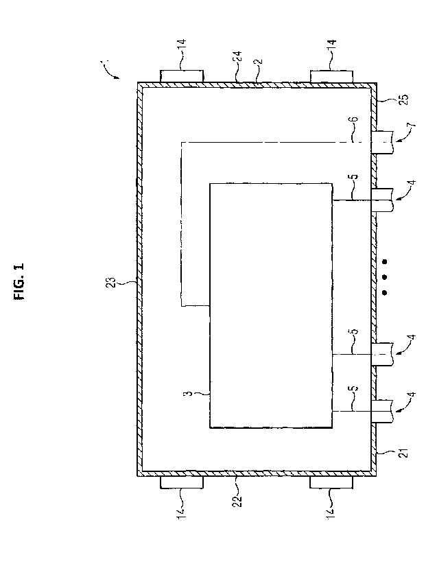
FIG 1
illustrates a modified RF power combiner 1 for RF
power combining or RF power splitting, in
accordance with aspects of the present technique.
Hereinafter, above-mentioned and other features of the
present technique are described in details. Various
embodiments are described with reference to the drawing,
wherein like reference numerals are used to refer to like
elements throughout. In the following description, for
purpose of explanation, numerous specific details are set
forth in order to provide a thorough understanding of one or
more embodiments. It may be noted that the illustrated
embodiments are intended to explain, and not to limit the
invention. It may be evident that such embodiments may be
practiced without these specific details.
In FIG 1 a modified RF power combiner 1 for RF power
combining or RF power splitting according to the present
invention is shown. The modified RF power combiner 1 is also
a modified RF power splitter, however for sake of simplicity
in the present disclosure only the term 'modified RF power
combiner' has been used for both RF power combining or RF
CA 069647 2017--132
WO 2016/089245 PCT/RU2014/000913
7
power splitting functions. The modified RF power combiner 1
includes a matching circuit 3, a plurality of first RF ports
4, exactly one second RF port 7 and a casing 2. The matching
circuit 3 is arranged inside the casing 2. The plurality of
first RF ports 4 and the second RF port 7 are arranged at a
first side 21 of the casing 2.
The first RF ports 4 are functionally distinct from the
second RF port 7 i.e. when the modified RF power combiner 1
is used to combine RF power or RF signal the first RF ports 4
act as input for RF signal into the modified RF power
combiner 1 and the second RF port 7 acts as output for RF
signal emanating from the modified RF power combiner 1.
Similarly, when the modified RF power combiner 1 is used to
split or divide RF power or RF signal the second RF port 7
act as input for RF signal into the modified RF power
combiner 1 and the first RF ports 4 acts as output for RF
signal emanating from the modified RF power combiner 1.
When the modified RF power combiner 1 is used to combine RF
power or RF signal, the matching circuit 3 is a RF power
combining circuit that accepts multiple input RF signals and
delivers a single RF output signal. The matching circuit 3 is
connected to the first RF ports 4. The matching circuit 3
receives RF power from two or more of the plurality of the
first RF ports 4 via inner conductors 5 of the first RF ports
4 and transforms the impedance of the received RF power to
impedance of a resultant single output. The resultant single
output exits the matching circuit 3 via a single transmission
line 6. The matching circuit 3 may be of various types, for
example zero-degree RF power combiners, and may have any
technical specification. Structure and operation of such
matching circuits 3 are well known in art of radio
technology, particularly in RF combiners, and thus has not
been described in details herein for sake of brevity.
Alternatively, when the modified RF power combiner 1 is used
to split RF power or RF signal, the matching circuit 3 is a
CA 069647 2017--132
WO 2016/089245 PCT/RU2014/000913
8
RF power splitting circuit that accepts single input RF
signal and delivers multiple RF output signals. The matching
circuit 3 is connected to the second RF port 7 via the single
transmission line 6. The matching circuit 3 receives RF power
from the second RF port 7 via the single transmission line 6
and transforms the impedance of the received RF power to
impedance of resultant multiple outputs. The resultant
multiple outputs exit the matching circuit 3 via the inner
conductors 5 and finally through the plurality of the first
RF ports 4. The matching circuit 3 may be of various types,
and may have any technical specification. Structure and
operation of such matching circuits 3 are well known in art
of radio technology, particularly in RF splitters, and thus
has not been described in details herein for sake of brevity.
It may be noted that in the present disclosure the term
'connected' or like phrases mean linked by a transmission
means such that RF power can transmit via the transmission
means. Thus when a first entity is said to be connected to a
second entity, then the first entity is linked to the second
entity via a transmission means, e.g. a RF conductor or a
wave guide such that RF power can transmit between the first
and the second entity via the transmission means. To explain
further, the matching circuit 3 is connected to the first RF
ports 4 means the matching circuit 3 is linked to the first
RF ports 4 via a transmission means, in this case the inner
conductors 5, such that RF power or RF signal is capable of
being transmitted between the matching circuit 3 and the
first RF ports 4. Thus, when a RF signal is received or
applied at the first RF ports 4, the received or applied RF
signal from the first RF ports 4 is transmitted to the
matching circuit 3 via the inner conductors 5. Furthermore,
when a RF signal exits or emanates from the matching circuit
3 in a direction towards the inner conductors 5, then the
emanating RF signal from the matching circuit 3 is
transmitted to the first RF ports 4 via the inner conductors
5.
CA 069647 2017--132
WO 2016/089245 PCT/RU2014/000913
9
Similarly, the matching circuit 3 is connected to the second
RF port 7 means the matching circuit 3 is linked to the
second RF port 7 via a transmission means, in this case the
single transmission line 6, such that RF power or RF signal
is capable of being transmitted between the matching circuit
3 and the second RF port 7. Thus, when a RF signal is
received or applied at the second RF port 7, the received or
applied RF signal from the second RF port 7 is transmitted to
the matching circuit 3 via the single transmission line 6.
Furthermore, when a RF signal exits or emanates from the
matching circuit 3 in a direction towards the single
transmission line 6, then the emanating RF signal from the
matching circuit 3 is transmitted to the second RF port 7 via
the single transmission line 6.
In the modified RF power combiner 1, the casing 2 encases or
encloses or houses the matching circuit 3 and the connections
between the matching circuit 3 and the first RF ports 4 and
the second RF port 7. The plurality of the first RF ports 4
and the second RF port 7 are arranged or located at the first
side 21 of the casing 2. In one embodiment of the modified RF
power combiner 1, the single transmission line 6 forms a 180
degree turn in between the matching circuit 3 and the second
RF port 7 thus enabling the positioning of the first RF ports
4 and the second RF port 7 on the same side of the casing 2
i.e. on the first side 21 of the casing 2.
The casing 2 is a covering or an enclosure and may have
varied shapes and sizes, for example the casing 2 may be, but
not limited to, a box, i.e. having a cuboidal shape,
cylindrical, hexagonal prism, and so on and so forth. When
the casing 2 is cuboidal in shape the first side 21 of the
casing 2 is one of the faces of the cuboid. As is depicted in
FIG 1, in a cross-section of the cubiodal casing 2, the first
RF ports 4 and the second RF port 7 are all located on the
first side 21 which forms exactly one face of the cubiodal
casing 2. The other sides 22,23,24 are devoid of the first RF
ports 4 and/or the second RF port 7. The casing 2 may be
CA 069647 2017--132
WO 2016/089245 PCT/RU2014/000913
formed of any suitable material used to house RF signal
processing devices or RF transmission lines, for example, the
casing 2 may be formed of metals, alloys, polymers, plastics,
and so on and so forth.
5
In one embodiment of the modified RF power combiner 1, the
plurality of the first ports 4 and the second port 7 are
embedded in a wall 25 of the casing 2 on the first side 21 of
the casing 2. The term 'embedded' as used herein means formed
10 within or entrenched in or implanted in. In the modified RF
power combiner 1, the wall 25 of the casing 2, along with the
plurality of the first ports 4 and the second port 7 embedded
in the wall 25, completely or fully covers or encloses a
volume (not shown). The matching circuit 3 is positioned in
the volume.
In one embodiment of the modified RF power combiner 1, the
matching circuit 3, the inner conductors 5 and the single
transmission line 6 are arranged within the casing 2 in such
a way that the matching circuit 3, the inner conductors 5 and
the single transmission line 6 are at fixed positions
relative to each other and to the casing 2. This is achieved
by fixing or fastening, for example by using screws, the
matching circuit 3, the inner conductors 5 and the single
transmission line 6 to the casing 2. Alternatively, the
modified RF power combiner 1 may be fabricated in a way that
matching circuit 3, the inner conductors 5 and the single
transmission line 6 are fabricated on a surface (not shown)
of the casing 2. One example of such fabrication is by
printing a circuit of the matching circuit 3, the inner
conductors 5 and the single transmission line 6 on the
surface of the casing 2.
In the embodiment of the modified RF power combiner 1, where
the casing 2 is cuboidal in shape, the cuboidal casing 2 is
adapted to be mountable inside a 19-inch rack. Such 19-inch
racks or 19-inch cabinets are well known and used prevalently
as standardized frame or enclosure for mounting multiple
CA 02969647 2017-06-02
WO 2016/089245 PCT/RU2014/000913
11
equipment modules. The dimensions of the casing 2 are such
that the casing 2, and thus the modified RF power combiner 1,
is compatible with the 19-inch racks i.e. the casing 2 and
thus the modified RF power combiner 1 is mountable in a 19-
inch rack as one of the modules. The casing 2 may
additionally include a mounting means 14 for mounting the
modified RF power combiner 1 inside a standard 19-inch rack.
In one embodiment of the modified RF power combiner 1, the
mounting means 14 is located on one or more of the other
sides 22,23,24 of the casing 2. The other sides 22,23,24 are
distinct from the first side 21 of the casing 2.
In an embodiment of the modified RF power combiner 1, the
mounting means 14 is a sliding means. In this embodiment, the
modified RF power combiner 1 is mountable inside a 19-inch
rack by slidingly engaging the sliding means with rails of
the 19-inch rack. Generally, a pair of rails is mounted or
fixed directly onto the 19-inch rack, and the modified RF
power combiner 1 then slides into the 19-inch rack along the
rails by contacting the rails of the 19-inch rack with the
sliding means of the casing 2. When in a desired position in
the 19-inch rack, the casing 2 may then be locked in the
desired position by an additional locking mechanism (not
shown) to the 19-inch rack. In another embodiment of the
modified RF power combiner 1, the mounting means 14 is a
fastening means for fixedly mounting the casing 2, and thus
the modified RF power combiner 1, inside the 19-inch rack.
The fastening means may be a bolt and screw mechanism or a
clicklock mechanism.
While the present technique has been described in detail with
reference to certain embodiments, it should be appreciated
that the present technique is not limited to those precise
embodiments. Rather, in view of the present disclosure which
describes exemplary modes for practicing the invention, many
modifications and variations would present themselves, to
those skilled in the art without departing from the scope and
spirit of this invention. The scope of the invention is,
CA 02969647 2017-06-02
WO 2016/089245 PCT/RU2014/000913
12
therefore, indicated by the following claims rather than by
the foregoing description. All changes, modifications, and
variations coming within the meaning and range of equivalency
of the claims are to be considered within their scope.