Note : Les descriptions sont présentées dans la langue officielle dans laquelle elles ont été soumises.
CA 02972953 2017-07-04
=
84022988
[DESCRIPTION]
[Invention Title]
BROADCAST SIGNAL TRANSMISSION APPARATUS, BROADCAST SIGNAL
RECEPTION APPARATUS, BROADCAST SIGNAL TRANSMISSION METHOD, AND
BROADCAST SIGNAL RECEPTION METHOD
[Technical Field]
[1] The present invention relates to a broadcast signal
transmitting apparatus, a broadcast signal receiving apparatus,
and broadcast signal transmitting and receiving methods.
[Background Art]
[2] As transmission of an analog broadcast signal ends,
various techniques for transmitting and receiving a digital
broadcast signal have been developed. The digital broadcast
signal can include more video/audio data than the analog
broadcast signal and further include various kinds of additional
data as well as the video/audio data.
[Disclosure]
[3] That is, a digital broadcasting system may provide
High Definition (HD) images, multi-channel audios, and various
additional services.
1
CA 02972953 2017-07-04
84022988
[4] For digital broadcasting, however, data transfer
efficiency for the transmission of a large amount of data, the
robustness of transmission/reception networks, and network
flexibility in which a mobile reception apparatus has been taken
into consideration need to be improved.
[5] Accordingly, an aspect of some embodiments is
directed to the provision of a method for maximizing a frequency
diversity effect using a different interleaving seed for each
OFDM symbol pair in a Frequency Interleaver (FT).
[6] Furthermore, another aspect of some embodiments is
directed to the provision of information indicating whether a
frequency interleaver is used in a broadcasting signal
transmission apparatus including the frequency interleaver.
[7] Technical effects to be achieved in this
specification are not limited to the aforementioned effects, and
those skilled in the art to which the present invention pertains
may evidently understand other technical effects from the
following description.
[7a] According to an aspect of the present invention,
there is provided a method of transmitting a broadcast signal,
the method comprising: formatting input streams into at least
one physical layer pipe (PLP); encoding data of the at least one
2
' 84022988
physical layer pipe (PLP); building a signal frame comprising
the encoded data; selectively performing frequency interleaving
on a data in the signal frame; modulating the signal frame by an
Orthogonal Frequency Division Multiplexing (OFDM) scheme; and
transmitting the broadcast signal comprising the signal frame,
wherein the signal frame comprises a preamble, wherein the
preamble includes control information indicating whether the
frequency interleaving on the data in the signal frame is
performed or not, when the control information is set to a first
value, the first value of the control information indicates that
the frequency interleaving is performed, and when the control
information is set to a second value, the second value of the
control information indicates that the frequency interleaving is
not performed.
(7b] According to another aspect of the present invention,
there is provided a transmission apparatus for transmitting a
broadcasting signal, the transmission apparatus comprising: an
input formatter for formatting input streams into at least one
physical layer pipe (PLP); an encoder for encoding data of the
at least one physical layer pipe (PLP); a framing and
interleaving module for building a signal frame comprising the
encoded data; a frequency interleaver for selectively performing
frequency interleaving on data in the signal frame; a modulator
2a
CA 2972953 2019-03-25
P =
84022988
for modulating the signal frame by an Orthogonal Frequency
Division Multiplexing (OFDM) method; and a transmitter for
transmitting a broadcast signal comprising the signal frame,
wherein the signal frame comprises a preamble, wherein the
preamble includes control information indicating whether the
frequency interleaving on the data in the signal frame is
performed or not, when the control information is set to a first
value, the first value of the control information indicates that
the frequency interleaving is performed, and when the control
information is set to a second value, the second value of the
control information indicates that the frequency interleaving is
not performed.
2b
CA 2972953 2019-05-06
CA 02972953 2017-07-04
7
[Technical Solution]
[8] In this specification, there is provided a method of
transmitting a broadcasting signal. The method includes
formatting input streams into at least one data transmission
charnel; encoding data corresponding to each of data
transmission channel carrying service data or service
component data; building at least one signal frame comprising
the encoded data; modulating the at least one signal frame by
an Orthogonal Frequency Division Multiplexing (OFDM) scheme;
and transmitting the broadcast signal comprising the at least
one modulated signal frame.
[9] Furthermore, in this specification, the signal frame
comprises a control information indicating whether a
frequency interleaver is used or not.
[10] Furthermore, in
this specification, the signal
frame further comprises a preamble carrying a physical layer
signaling data, and wherein the control information is
included in the preamble.
[11] Furthermore, in
this specification, the building
the at least one signal frame comprises frequency
interleaving the data included in the at least one signal
frame, the frequency interleaving is performed using a
3
CA 02972953 2017-07-04
different interleaving seed for each OFDM symbol pair, two
types of memory are used for the frequency interleaving, and
the OFDM symbol pair comprises two sequential OFDM symbols.
[12] Furthermore, in
this specification, the frequency
interleaving comprises frequency interleaving on an even-
numbered OFDM symbol pair and an odd-numbered OFDM symbol
pair through different types of memory, and different
interleaving seeds are used for the even-numbered OFDM symbol
pair and the odd-numbered OFDM symbol pair.
[13] Furthermore, in this specification, the frequency
interleaving is performed through interleaving seeds
respectively generated by a first interleaving sequence
generator and a second interleaving sequence generator.
[14] Furthermore, in this specification, the different
interleaving seed used in each OFDM symbol pair is generated
using a cyclic shift value, and wherein the cyclic shift
value is a symbol offset value generated by the second
interleaving sequence generator.
[15] Furthermore, in this specification, the control
information is frequency interleaver mode (FT MODE)
information.
4
. .
84022988
[16] Furthermore, in this specification, there is
provided a transmission apparatus for transmitting a
broadcasting signal, comprising an input formatter for
formatting input streams into at least one data transmission
channel; an encoder for encoding data corresponding to each of
data transmission channel which carrying service data or service
component data; a framing & interleaving module for building at
least one signal frame comprising the encoded data; a modulator
for modulating the at least one signal frame by an Orthogonal
Frequency Division Multiplexing (OFDM) method; and a transmitter
for transmitting a broadcast signal comprising the at least one
modulated signal frame, wherein the framing & interleaving
module comprises a frequency interleaver for frequency
interleaving the data included in the at least one signal frame,
wherein the signal frame comprises a control information
indicating whether a frequency interleaver is used or not.
[17] An embodiment of the present invention can provide
various broadcasting services by processing data according to
service characteristics and controlling Quality of Service (QoS)
for each service or service component.
5
CA 2972953 2019-05-06
CA 02972953 2017-07-04
4
[18] Furthermore,
an embodiment of the present
invention can achieve transmission flexibility by
transmitting various broadcasting services through the same
Radio Frequency (RF) signal bandwidth.
[19] Furthermore, an
embodiment of the present
invention can improve data transfer efficiency and the
transmission/reception robustness of a broadcasting signal
using a Multiple-Input Multiple-Output (MIMO) system.
[20] Furthermore,
an embodiment of the present
invention can provide the broadcast signal
transmission/reception methods and apparatuses, wherein a
digital broadcast signal can be received without an error
although a mobile reception apparatus is used or an indoor
environment.
[21] Furthermore, this
specification is advantageous in
that a frequency diversity effect can be maximized using a
different interleaving seed for each OFDM symbol pair in the
frecuency interleaver (FI).
[22] Furthermore,
this specification is advantageous in
that it can improve data restoration speed by transmitting
information indicating whether a frequency interleaver has
been used through a preamble in advance so that the broadcast
signal reception apparatus is previously aware of whether
6
CA 02972953 2017-07-04
0
frequency interleaving has been performed on a received
signal prior to data decoding.
[23] Furthermore, this specification is advantageous in
that it can support FDM by turning off an Fl operation
through the operation of Fl mode information for turning on
or off the Fl operation.
[24] Advantages to be obtained in this specification
are not limited to the aforementioned advantages and may
include various other advantages that are evident to those
skilled in the art to which the present invention pertains
from the following description.
[Description of Drawings]
[25] The accompanying drawings included to more
IF) appreciate the present invention and included in the present
application, and constituting a part thereof illustrate
embodiments of the present invention together with a detailed
description for describing a principle the present invention.
FIG. 1 illustrates a structure of a broadcast signal
transmitting apparatus for a next-generation broadcasting
service according to an exemplary embodiment of the present
invention.
7
GA 02972953 2017-07-04
FIG. 2 illustrates an input formatting block according
to an exemplary embodiment of the present invention.
FIG. 3 illustrates an input formatting block according
to another exemplary embodiment of the present invention.
FIG. 4 illustrates an input formatting block according
to yet another exemplary embodiment of the present invention.
FIG. 5 illustrates a bit interleaved coding &
modulation (BICM) block according to an exemplary embodiment
of the present invention.
FIG. 6 illustrates a BICM block according to another
exemplary embodiment of the present invention.
FIG. 7 illustrates a frame building block according to
an exemplary embodiment of the present invention.
FIG. 8 illustrates an orthogonal frequency division
multiplexing (OFDM) generation block according to an
exemplary embodiment of the present invention.
FIG. 9 illustrates a structure of a broadcast signal
receiving apparatus for a next-generation broadcasting
service according to an exemplary embodiment of the present
invention.
8
CA 02972953 2017-07-04
FIG. 10 illustrates a frame structure according to an
exemplary embodiment of the present invention.
FIG. 11 illustrates a signaling layer structure of a
frame structure according to an exemplary embodiment of the
present invention.
FIG. 12 illustrates preamble signaling data according
to an exemplary embodiment of the present invention.
FIG. 13 illustrates PLS1 data according to an exemplary
embodiment of the present invention.
FIG. 14 illustrates PLS2 data according to an exemplary
embodiment of the present invention.
FIG. 15 illustrates PLS2 data according to another
exemplary embodiment of the present invention.
FIG. 16 illustrates a logical structure of a frame
according to an exemplary embodiment of the present invention.
FIG. 17 illustrates physical layer signaling (FLS)
mapping according to an exemplary embodiment of the present
invention.
FIG. 18 illustrates emergency alert channel (EAC)
mapping according to an exemplary embodiment of the present
9
CA 02972953 2017-07-04
invention.
FIG. 19 illustrates fast information channel (FTC)
mapping according to an exemplary embodiment of the present
invention.
FIG. 20 illustrates a type of data pipe (DP) according
to an exemplary embodiment of the present invention.
FIG. 21 illustrates a type of data pipe (DP) mapping
according to an exemplary embodiment of the present invention.
FIG. 22 illustrates forward error correction (FEC)
structure according to an exemplary embodiment of the present
invention.
FIG. 23 illustrates bit interleaving according to an
exemplary embodiment of the present invention.
FIG. 24 illustrates cell-word demultiplexing according
an exemplary embodiment of the present invention.
FIG. 25 illustrates time interleaving according to an
exemplary embodiment of the present invention.
FTC. 26 illustrates a basic operation of a twisted row-
column block interleaver according to an exemplary embodiment
of the present Invention.
CA 02972953 2017-07-04
=
FIG. 27 illustrates an operation of a twisted row-
column block interleaver according to another exemplary
embodiment of the present invention.
FIG. 28 illustrates a diagonal reading pattern of the
twisted row-column block interleaver according to the
exemplary embodiment of the present Invention.
FIG. 29 illustrates XFECBLOCK interleaved from each
interleaving array according to an exemplary embodiment of
the present invention.
FIG. 30 is a diagram illustrating one example of a
synchronization and demodulation module of FIG. 9.
FIG. 31 is a diagram illustrating one example of a
frame parsing module of FIG. 9.
FIG. 32 is a diagram illustrating one example of a
demapping and decoding module of FIG. 9.
FIG. 33 is a diagram illustrating one example of one
example of an output processor of FIG. 9.
FIG. 34 is a diagram illustrating another example of
the output processor of FIG. 9.
FIG. 35 illustrates a coding and modulation module
11
CA 02972953 2017-07-04
=
according to another exemplary embodiment of the present
invention.
FiG. 36 is a diagram illustrating a demapping and
decoding module according to another exemplary embodiment of
the present invention.
FIG. 37 is a diagram illustrating another structure of
the broadcasting signal transmission apparatus for a next-
generation broadcasting service in accordance with an
embodiment of the present invention.
FIG. 38 is a diagram illustrating a simplified TDM
broadcasting transmission system and LDM broadcasting
transmission system in accordance with an embodiment of the
present invention.
FIG. 39 Illustrates a framing & interleaving block in
accordance with an embodiment of the present invention.
FIG_ 40 is a diagram illustrating an example of an ATSC
3.0 frame structure to which an embodiment of the present
invention may be applied.
FIG. 41 is a diagram illustrating another example of
the frame building block of FIG. 7.
12
CA 02972953 2017-07-04
FIG. 42 is a diagram illustrating an example of a
preamble format to which an embodiment of the present
invention may be applied.
FIG. 43 is a diagram illustrating another internal
block diagram of the frame parsing block of FIG. 31.
FIG. 44 is a diagram illustrating the operation of a
frequency interleaver in accordance with an embodiment of the
present invention.
FIG. 45 illustrates the basic switch model of MUX and
DEMUX methods in accordance with an embodiment of the present
inwmtion_
FIG. 46 illustrates the operation of a memory bank in
accordance with an embodiment of the present invention.
FIG. 47 is a diagram illustrating a frequency
interleaving process in accordance with an embodiment of the
present invention.
FIG. 48 Illustrates a conceptual diagram of frequency
interleaving abplied to a single super frame in accordance
with an embodiment of the present invention.
FIG. 49 is a diagram illustrating the logical operation
13
CA 02972953 2017-07-04
1
mechanism of frequency Interleaving applied to a single super
frame proposed in this specification.
FIG. SO illustrates the equation of the logical
operation mechanism of frequency interleaving applied to a
single super frame in accordance with an embodiment of the
present Invention.
FIG. 51 is a diagram illustrating the logical operation
mechanism of frequency interleaving applied to a single
signal frame in accordance with an embodiment of the present
invention.
FIG. 52 illustrates the equation of the logical
operation mechanism of frequency interleaving applied to a
single super frame in accordance with an embodiment of the
present invention.
FIG. 53 is a diagram illustrating the single memory
deinterleaving of input-sequential OFDM symbols which is
proposed in this specification.
FIG. 54 is a flowchart illustrating an example of a
method of transmitting a broadcasting signal which is
proposed in this specification.
FIG. 55 is a flowchart illustrating an example of a
14
CA 02972953 2017-07-04
method of receiving a broadcasting signal which is proposed
in this specification.
[Best Mode]
[26] Reference will now be made in detail to the
preferred embodiments of the present invention, examples of
which are illustrated in the accompanying drawings. The
detailed description, which will be given below with
reference to the accompanying drawings, is intended to
explain exemplary embodiments of the present invention,
rather than to show the only embodiments that can be
implemented according to the present invention. The
following detailed description includes specific details in
order to provide a thorough understanding of the present
invention. However, it will be apparent to those skilled in
the art that the present invention may be practiced without
such specific details.
[27] Although most terms used in the present invention
have been selected from general ones widely used in the art,
some terms have been arbitrarily selected by the applicant
and their meanings are explained in detail in the following
description as needed. Thus, the present invention should be
understood based upon the intended meanings of the terms
CA 02972953 2017-07-04
rather than their simple names or meanings.
[28] The present Invention provides apparatuses and
methods for transmitting and receiving broadcast signals for
future broadcast services. Future broadcast services
according to an embodiment of the present invention include a
terrestrial broadcast service, a mobile broadcast service, a
UHDTV service, etc. The present
invention may process
broadcast signals for the future broadcast services through
non-MIMO (Multiple Input Multiple Output) or MIMO according
to one embodiment. A non-MIMO scheme
according to an
embodiment of the present invention may include a MISO
(Multiple Input Single Output) scheme, a SISO (Single Input
Single Output) scheme, etc.
[29] While MISO or MIMO uses two antennas in the
following for convenience of description, the present
invention is applicable to systems using two or more antennas.
The present invention may defines three physical layer (PL)
profiles - base, handheld and advanced profiles-each
optimized to minimize receiver complexity while attaining the
performance required for a particular use case. The physical
layer (PHY) profiles are subsets of all configurations that a
corresponding receiver should implement.
[30] The three PHY profiles share most of the
16
CA 02972953 2017-07-04
functional blocks but differ slightly in specific blocks
and/or parameters. Additional PHI profiles can be defined in
the future. For the system evolution, future profiles can
also be multiplexed with the existing profiles in a single RF
channel through a future extension frame (FEF). The details
of each PHI profile are described below.
[31] 1. Base profile
[32] The base profile represents a main use case for
fixed receiving devices that are usually connected to a roof-
top antenna. The base profile also includes portable devices
that could be transported to a place but belong to a
relatively stationary reception category. Use of the base
profile could be extended to handheld devices or even
vehicular by some improved implementations, but those use
cases are nor expected for the base profile receiver
operation.
[33] Target SNR range of reception is from
approximately 10 to 20dB, which includes the 15dB SNR
reception capability of the existing broadcast system (e.g.
ATSC A/53). The receiver complexity and power consumption is
not as critical as in the battery-operated handheld devices,
which will use the handheld profile. Key system parameters
for the base profile are listed in below table 1.
17
CA 02972953 2017-07-04
[34] [Table A
LDPC codeword length 16K, 64K bits
Constellation size 4-10 bpcu (bits per channel use)
Time de-interleaving memory size 2'9 data cells
Pilot patterns Pilot pattern for fixed
reception
FFT size 16K, 32K points
[35] 2. Handheld profile
[36] The handheld profile is designed for use in
handheld and vehicular devices that operate with battery
power. The devices can be moving with pedestrian or vehicle
speed. The power consumption as well as the receiver
complexity is very important for the implementation of the
devices of the handheld profile. The target SNR range of the
handheld profile is approximately 0 to 10dB, but can be
configured to reach below OdB when intended for deeper indoor
reception.
[37] In addition to low SNR capability, resilience to
the Doppler Effect caused by receiver mobility is the most
important performance attribute of the handheld profile. Key
system parameters for the handheld profile are listed in the
below table 2.
[38] [Table 2]
18
CA 02972953 2017-07-04
LDPC codeword length 16 Kbits
Constellation size 2-8 bpcu
Time de-interleaving memory size 21E' data cells
Pilot patterns Pilot patterns for mobile and
indoor reception
FFT size 8K, 16K points
[39] 3. Advanced profile
[40] The advanced profile provides highest channel
capacity at the cost of more implementation complexity. This
profile requires using AIM transmission and reception, and
UHDTV service is a target use case for which this profile is
specifically designed. The increased capacity can also be
used to allow an increased number of services in a given
bandwidth, e.g., multiple SDTV or HDTV services.
[41] The target SNR range of the advanced profile is
approximately 20 to 30dB. HIMO transmission may initially use
existing elliptically-polarized transmission equipment, with
extension to full-power cross-polarized transmission in the
future. Key system parameters for the advanced profile are
listed in below table 3.
[42] [Table 3]
LDPC codeword length 16K, 64Kbits
Constellation size 8-12 bpcu
Time de-interleaving memory size 219 data cells
19
CA 02972953 2017-07-04
Pilot patterns Pilot pattern for fixed
reception
FFT size 16K, 32K points
[43] In this case,
the base profile can be used as a
profile for both the terrestrial broadcast service and the
mobile broadcast service. That is, the base profile can be
used to define a concept of a profile which includes the
mobile profile. Also, the advanced profile can be divided
advanced profile for a base profile with MIMO and advanced
profile for a handheld profile with MIMO. Moreover, the three
profiles can be changed according to intention of the
designer.
[44] The following terms and definitions may apply to
the present invention. The following terms and definitions
can be changed according to design.
[45] auxiliary stream: sequence of cells carrying data
of as yet undefined modulation and coding, which may be used
for future extensions or as required by broadcasters or
network operators
[46] base data pipe: data pipe that carries service
signaling data
[47] baseband frame (or BBFRAME): set of Kbch bits
which form the input to one FEC encoding process (BCH and
CA 02972953 2017-07-04
LDPC encoding)
[48] cell: modulation value that is carried by one
carrier of the OFDM transmission
[49] coded block: LDPC-encoded block of PLS1 data or
one of the LDPC-encoded blocks of PLS2 data
[50] data pipe: logical channel in the physical layer
that carries service data or related metadata, which may
carry one or multiple service(s) or service component(s).
[51] The data pipe can be represented to a data
.. transmission channel.
[52] data pipe unit: a basic unit for allocating data
cells to a DP in a frame.
[53] data symbol: OFDM symbol in a frame which is not a
preamble symbol (the frame signaling symbol and frame edge
symbol is included in the data symbol)
[54] DP_ID: this 8-bit field identifies uniquely a DP
within the system identified by the SYSTEM ID
[55] dummy cell: cell carrying a pseudo-random value
used to fill the remaining capacity not used for PLS
.. signaling, DPs or auxiliary streams
[56] emergency alert channel: pail_ of a frame that
carries ES information data
[57] frame: physical layer time slot that starts with a
21
GA 02972953 2017-07-04
preamble and ends with a frame edge symbol
[58] frame repetition unit: a set of frames belonging
to same or different physical layer profile including a FEF,
which is repeated eight times in a super-frame
[59] fast information channel: a logical channel in a
frame that carries the mapping information between a service
and the corresponding base DP
[60] FECBLOCK: set of LDPC-encoded bits of a DP data
[61] FFT size: nominal FFT size used for a particular
mode, equal to the active symbol period Ts expressed in
cycles of the elementary period T
[62] frame signaling symbol: OFDM symbol with higher
pilot density used at the start of a frame in certain
combinations of FFT size, guard interval and scattered pilot
pattern, which carries a part of the PLS data
[63] frame edge symbol: OFDM symbol with higher pilot
density used at the end of a frame in certain combinations of
FFT size, guard interval and scattered pilot pattern
[64] frame-group: the set of all the frames having the
same PHY profile type in a super-frame.
[65] future extension frame: physical layer time slot
within the super-frame that could be used for future
extension, which starts with a preamble
22
CA 02972953 2017-07-04
[66] Futurecast UTE system: proposed physical layer
broadcasting system, of which the input is one or more MPEG2-
TS or IF or general stream(s) and of which the output is an
RF signal
[67] input stream: A stream of data for an ensemble of
services delivered to the end users by the system.
[68] normal data symbol: data symbol excluding the
frame signaling symbol and the frame edge symbol
[69] PHY profile: subset of all configurations that a
corresponding receiver should implement
[70] PLS: physical layer signaling data consisting of
PLS1 and PLS2
[71] PLSI: a first set of PLS data carried in the FSS
symbols having a fixed size, coding and modulation, which
carries basic information about the system as well as the
parameters needed to decode the PLS2
[72] NOTE: PLS1 data remains constant for the duration
of a frame-group.
[73] PLS2: a second set of PLS data transmitted in the
FSS symbol, which carries more detailed PLS data about the
system and the DPs
[74] PLS2 dynamic data: PLS2 data that may dynamically
change frame-by--frame
23
CA 02972953 2017-07-04
[75] PLS2 static data: PLS2 data that remains static
for the duration of a frame-group
[76] preamble signaling data: signaling data carried by
the preamble symbol and used to identify the basic mode of
the system
[77] preamble symbol: fixed-length pilot symbol that
carries basic ?LS data and is located in the beginning of a
frame
[78] NOTE: The preamble symbol is mainly used for fast
initial band scan to detect the system signal, its timing,
frequency offset, and FFT-size.
[79] reserved for future use: not defined by the
present document but may be defined in future
[80] super-frame: set of eight frame repetition units
[81] time intcrlcaving block (TI block): set of cells
within which time interleaving is carried out, corresponding
to one use of the time interleaver memory
[82] TI group: unit over which dynamic capacity
allocation for a particular DP is carried out, made up of an
integer, dynamically varying number of XFECBLOCKs
[83] NOTE: The TI group may be mapped directly to one
frame or may be mapped to multiple frames. It may contain one
or more TI blocks.
24
CA 02972953 2017-07-04
[84] Type 1 DP: DP of a frame where all DPs are mapped
into the frame in TDM fashion
[85] Type 2 DP: DP of a frame where all DPs are mapped
intc the frame in FDM fashion
[86] XFECBLOCK: set of Ncells cells carrying all the
bits of one LDPC FECBLOCK
[87] Block interleaver: An interleaver where the input
data is written along the rows of a memory configured as a
matrix, and read out along the columns.
[88] Cell interleaver: An interleaver operating at the
cell level.
[89] Interleaver: A device used in conjunction with
error correcting codes to counteract the effect of burst
errors.
[90] Physical Layer Pipe(PLP): A structure specified to
an allocated capacity and robustness that can be adjusted to
broadcaster needs.
[91] The PLP is represented to a data pipe or data
transmission channel.
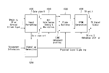
[92] FIG. 1 illustrates a structure of an apparatus for
transmitting broadcast signals for future broadcast services
according to an embodiment of the present invention.
[93] The apparatus for transmitting broadcast signals
84022988
for future broadcast services according to an embodiment of
the present invention can include an input formatting block
1000, a BICM (Bit interleaved coding & modulation) block 1010,
a frame building block 1020, an OFDM (Orthogonal Frequency
Division Multiplexing) generation block 1030 and a signaling
generation block 1040.
[94] A
description will be given of the operation of
each module of the apparatus for transmitting broadcast
signals.
[95] The input
formatting block 1000 can be represented
to an input formatter.
[96] The BICH (Bit interleaved coding & modulation)
block 1010 can be represented to an encoder.
[97] The frame building block 1020 can be represented
to a frame builder or a frame building block or a framing &
interleaving block.
[98] The OFDM
(Orthogonal Frequency Division
Multiplexing) generation block 1030 can be represented to a
modulator.
70 [99] IP
stream/packets and MPEG2-TS are the main input
formats, other stream types are handled as General Streams.
In addition to these data inputs, Management Information is
input to control the scheduling and allocation of the
26
CA 2972953 2018-10-03
CA 02972953 2017-07-04
corresponding bandwidth for each input stream. One or
multiple TS stream(s), IF stream(s) and/or General Stream(s)
inputs are simultaneously allowed.
[100] The input formatting block 1000 can demultiplex
each input stream into one or multiple data pipe(s), to each
of which an independent coding and modulation is applied. The
data pipe (DO) is the basic unit for robustness control,
thereby affecting quality-of-service (QoS). One or multiple
service(s) or service component(s) can be carried by a single
DP. Details of operations of the input formatting block 1000
will be described later.
[101] The data pipe is represented to the data
transmission(or transport) channel or the PLP.
[102] The data pipe is a logical channel in the physical
.. laycr that carrier ocrvicc data or rclatcd mctadata, which
may carry one or multiple service(s) or service component(s).
[103] The data pipe can be represented to a data
transmission channel.
[104] Also, the data pipe unit: a basic unit for
allocating data cells to a DP in a frame.
[105] In the BICM block 1010, parity data is added for
error correction and the encoded bit streams are mapped to
complex-value constellation symbols. The symbols are
27
CA 02972953 2017-07-04
interleaved across a specific interleaving depth that is used
for the corresponding DP. For the advanced profile, MIMO
encoding is performed in the BICM block 1010 and the
additional data path is added at the output for MIMO
transmission. Details of operations of the BICM block 1010
will be described later.
[106] The Input Formatting Block of FIG. 1 implements
functions, processes, and/or methods proposed in FIGS. 50, 51,
and 52 to be described below.
[107] The Frame Building block 1020 can map the data
cells of the input DPs into the OFDM symbols within a frame.
After mapping, the frequency interleaving is used for
frequency-domain diversity, especially to combat frequency-
selective fading channels. Details of operations of the Frame
Building block 1020 will be described later_
[108] After inserting a preamble at the beginning of
each frame, the OFDM Generation block 1030 can apply
conventional OFDM modulation having a cyclic prefix as guard
interval. For antenna space diversity, a distributed MISO
scheme is applied across the transmitters. In addition, a
Peak-to-Average Power Reduction (PAPR) scheme is performed in
the time domain. For flexible network planning, this proposal
provides a set of various FFT sizes, guard interval lengths
28
CA 02972953 2017-07-04
and corresponding pilot patterns. Details of operations of
the OFDM Generation block 1030 will be described later.
[109] The Signaling Generation block 1040 can create
physical layer signaling information used for the operation
.. of each functional block. This signaling information is also
transmitted so that the services of Interest are properly
recovered at the receiver side. Details of operations of the
Signaling Generation block 1040 will be described later.
[110]
[111] FIGS. 2, 3 and 4 Illustrate the input formatting
block 1000 according to embodiments of the present invention.
A description will be given of each figure.
[112] The Input Formatting Block of FIG. 2 to Fig. 4
implements functions, processes, and/or methods proposed in
FIGS. 50, 51, and 52 to be described below.
[113] FIG. 2 illustrates an input formatting block
according to one embodiment of the present invention. FIG. 2
shows an input formatting module when the input signal is a
single input stream.
[114] The input formatting block illustrated in FIG. 2
corresponds to an embodiment of the input formatting block
1000 described with reference to FIG. 1.
[115] The input to the physical layer may be composed of
29
CA 02972953 2017-07-04
one or multiple data streams. Each data stream is carried by
one DP. The mode adaptation modules slice the incoming data
stream into data fields of the baseband frame (BBF). The
system supports three types of input data streams: MPEG2-TS,
.. Internet protocol (IP) and Generic stream (GS). MPEG2-TS is
characterized by fixed length (188 byte) packets with the
first byte being a sync-byte (0x47). An IP stream is composed
of variable length IP datagram packets, as signaled within IP
packet headers. The system supports both IPv4 and IPv6 for
the IP stream. GS may be composed of variable length packets
or constant length packets, signaled within encapsulation
packet
[116] (a) shows a mode adaptation block 2000 and a
stream adaptation 2010 for signal DP and (b) shows a PLS
generation block 2020 and a PLS scrambler 2030 for generating
and processing PLS data. A description will be given of the
operation of each block.
[117] The Input Stream Splitter splits the input IS, IP,
GS streams into multiple service or service component (audio,
video, etc.) streams. The mode adaptation module 2010 is
comprised Of a CRC Encoder, BE (baseband) Frame Slicer, and
BB Frame Header Insertion block.
[118] The CRC Encoder provides three kinds of CRC
CA 02972953 2017-07-04
encoding for error detection at the user packet (UP) level,
i.e., CRC-8, CRC-16, and CRC-32. The computed CRC bytes are
appended after the UP. CRC-8 is used for TS stream and CRC-32
for IP stream. If the GS stream doesn't provide the CRC
encoding, the proposed CRC encoding should be applied.
[119] BB Frame Slicer maps the Input into an internal
logical-bit format. The first received bit is defined to be
the MSB. The BB Frame Slicer allocates a number of input bits
equal to the available data field capacity. To allocate a
number of input bits equal to the BBF payload, the UP packet
stream is sliced to fit the data field of BBF.
[120] BB Frame Header Insertion block can insert fixed
length BBF header of 2 bytes is inserted in front of the BB
Frame. The BBF header is composed of STUFFI (1 bit), SYNCD
(13 bits), and RFU (2 bits). In addition to the fixed 2-Byte
BBF header, BBF can have an extension field (1 or 3 bytes) at
the end of the 2-byte BBF header.
[121] The stream adaptation 2010 is comprised of
stuffing insertion block and BB scrambler.
[122] The stuffing insertion block can insert stuffing
field into a payload of a BE frame. If the input data to the
stream adaptation is sufficient to fill a BB-Frame, STUFFI is
set to '0' and the BBF has no stuffing field. Otherwise
31
CA 02972953 2017-07-04
STUFFI is set to '1' and the stuffing field is inserted
immediately after the BDF header. The stuffing field
comprises two bytes of the stuffing field header and a
variable size of stuffing data.
[123] The BB scrambler scrambles complete BBF for energy
dispersal. The scrambling sequence is synchronous with the
BBF. The scrambling sequence is generated by the feed-back
shift register.
[124] The PLS generation block 2020 can generate
physical layer signaling (PLS) data. The PLS provides the
receiver with a means to access physical layer DPs. The PLS
data consists of PLS1 data and PLS2 data.
[125] The PLS1 data is a first set of PLS data carried
in the FSS symbols in the frame having a fixed size, coding
.. and modulation, which carries basic information about the
system as well as the parameters needed to decode the PLS2
data. The PLS1 data provides basic transmission parameters
including parameters required to enable the reception and
decoding of the PLS2 data. Also, the PLS1 data remains
.. constant for the duration of a frame-group.
[126] The PLS2 data is a second set of PLS data
transmitted in the FSS symbol, which carries more detailed
PLS data about the system and the DPs. The PLS2 contains
32
CA 02972953 2017-07-04
parameters that provide sufficient information for the
receiver to decode the desired DP. The PLS2 signaling further
consists of two types of parameters, PLS2 Static data (PLS2-
STAT data) and PLS2 dynamic data (PLS2-DYN data). The PLS2
Static data is PLS2 data that remains static for the duration
of a frame-group and the PLS2 dynamic data is PLS2 data that
may dynamically change frame-by-frame.
[127] Details of the PLS data will be described later.
[128] The PLS scrambler 2030 can scramble the generated
.. PLS data for energy dispersal.
[129] The above-described blocks may be omitted or
replaced by blocks having similar or identical functions.
[130]
[131] FIG. 3 illustrates an input formatting block
according to another embodiment of the present invention.
[132] The input formatting block illustrated in FIG. 3
corresponds to an embodiment of the input formatting block
1000 described with reference to FIG. 1.
[133] FIG. 3 shows a mode adaptation block of the input
formatting block when the input signal corresponds to
multiple input streams.
[134] The mode adaptation block of the input formatting
block for processing the multiple input streams can
33
CA 02972953 2017-07-04
independently process the multiple input streams.
[135] Referring to FIG. 3, the mode adaptation block for
respectively processing the multiple input streams can
include an input stream splitter 3000, an input stream
synchronizer 3010, a compensating delay block 3020, a null
packet deletion block 3030, a head compression block 3040, a
CRC encoder 3050, a BB frame slicer 3060 and a BB header
insertion block 3070. Description will be given of each
block of the mode adaptation block.
[136] Operations of the CRC encoder 3050, BB frame
slicer 3060 and BB header insertion block 3070 correspond to
those of the CRC encoder, BB frame slicer and BB header
insertion block described with reference to FIG. 2 and thus
description thereof is omitted.
[137] The input stream splitter 3000 can split thc input
TS, IP, GS streams into multiple service or service component
(audio, video, etc.) streams.
[138] The input stream synchronizer 3010 may be referred
as ISSY. The ISSY can provide suitable means to guarantee
Constant Bit Rate (CBR) and constant end-to-end transmission
delay for any input data Lomat. The ISSY is always used for
the case of multiple DPs carrying TS, and optionally used for
multiple DPs carrying GS streams.
34
CA 02972953 2017-07-04
[139] The compensating delay block 3020 can delay the
split TS packet stream following the insertion of ISSY
information to allow a TS packet recombining mechanism
without requiring additional memory in the receiver.
[140] The null packet deletion block 3030, is used only
for the TS input stream case. Some TS input streams or split
TS streams may have a large number of null-packets present in
order to accommodate VBR (variable bit-rate) services in a
CBR TS stream. In this case, in order to avoid unnecessary
transmission overhead, null-packets can be identified and not
transmitted. In the receiver, removed null-packets can be re-
inserted in the exact place where they were originally by
reference to a deleted null-packet (DNP) counter that is
inserted in the transmission, thus guaranteeing constant bit-
rate and avoiding the need for time-stamp (PCR) updating.
[141] The head compression block 3040 can provide packet
header compression to increase transmission efficiency for TS
or IP input streams. Because the receiver can have a priori
information on certain parts of the header, this known
information can be deleted in the transmitter.
[142] For Transport Stream, the receiver has a-priori
information about the sync-byte configuration (0x47) and the
packet length (188 Byte). If the input TS stream carries
GA 02972953 2017-07-04
content that has only one PID, i.e., for only one service
component (video, audio, etc.) or service sub-component (SVC
base layer, SVC enhancement layer, MVC base view or MVC
dependent views), TS packet header compression can be applied
(optionally) to the Transport Stream. IP packet header
compression is used optionally if the input steam is an IF
stream.
[143] The above-described blocks may be omitted or
replaced by blocks having similar or identical functions.
[144]
[145] FIG. 4 illustrates an input formatting block
according to another embodiment of the present invention.
[146] The input formatting block illustrated in FIG. 4
corresponds to an embodiment of the input formatting block
1000 described with reference to FIG. 1.
[147] FIG. 4 illustrates a stream adaptation block of
the input formatting module when the input signal corresponds
to multiple input streams.
[148] Referring to FIG. 4, the mode adaptation block for
respectively processing the multiple input streams can
include a scheduler 4000, an 1-Frame delay block 4010, a
stuffing insertion block 4020, an in-band signaling 4030, a
BB Frame scrambler 4040, a PLS generation block 4050 and a
36
CA 02972953 2017-07-04
PLS scrambler 4060. Description will be given of each block
of the stream adaptation block.
[149] Operations of the stuffing insertion block 4020,
the BB Frame scrambler 4040, the PLS generation block 4050
and the PLS scrambler 4060 correspond to those of the
stuffing insertion block, BB scrambler, PLS generation block
and the PLS scrambler described with reference to FIG. 2 and
thus description thereof is omitted.
[150] The scheduler 4000 can determine the overall cell
allocation across the entire frame from the amount of
FECELOCKs of each DP. Including the allocation for PLS, EAC
and FIC, the scheduler generate the values of PLS2-DYN data,
which is transmitted as in-band signaling or PLS cell in FSS
of the frame. Details of FFCBLOCK, EAC and FIC will be
13 described later.
[151] The 1-Frame delay block 4010 can delay the input
data by one transmission frame such that scheduling
information about the next frame can be transmitted through
the current frame for in-band signaling information to be
inserted into the DPs.
[152] The in-band signaling 4030 can insert un-delayed
part of the PLS2 data into a DP of a frame.
[153] The above-described blocks may be omitted or
37
CA 02972953 2017-07-04
replaced by blocks having similar or identical functions.
[154]
[155] FIG. 5 illustrates a BICM block according to an
embodiment of the present invention.
[156] The BICM block illustrated in FIG. 5 corresponds
to an embodiment of the BICM block 1010 described with
reference to FIG. 1.
[157] As described above, the apparatus for transmitting
broadcast signals for future broadcast services according to
an embodiment of the present invention can provide a
terrestrial broadcast service, mobile broadcast service,
UADTV service, etc.
[158] Since QoS (quality of service) depends on
characteristics of a service provided by the apparatus for
.. transmitting broadcast signals for future broadcast services
according to an embodiment of the present invention, data
corresponding to respective services needs to be processed
through different schemes. Accordingly, the a BICM block
according to an embodiment of the present invention can
independently process DPs input thereto by independently
applying SISO, MIS() and MIMO schemes to the data pipes
respectively corresponding to data paths. Consequently, the
apparatus for transmitting broadcast signals for future
38
CA 02972953 2017-07-04
broadcast services according to an embodiment of the present
invention can control QoS for each service or service
component transmitted through each DP.
[159] (a) shows the BICM block shared by the base
profile and the handheld profile and (b) shows the BICM block
of the advanced profile.
[160] The BICM block shared by the base profile and the
handheld profile and the BICM block of the advanced profile
can include plural processing blocks for processing each DP.
[161] A description will be given of each processing
block of the BICM block for the base profile and the handheld
profile and the BICM block for the advanced profile.
[162] A processing block 5000 of the BICM block for the
base profile and the handheld profile can include a Data FEC
encoder 5010, a bit interleaver 5020, a constellation mapper
5030, an SSD (Signal Space Diversity) encoding block 5040 and
a time interleaver 5050.
[163] The Data FEC encoder 5010 can perform Lhe FEC
encoding on the input BBF to generate FECBLOCK procedure
using outer coding (BCH), and inner coding (LDPC). The outer
coding (BCH) is optional coding method. Details of operations
of the Data FEC encoder 5010 will be described later.
[164] The bit interleaver 5020 can interleave outputs of
39
CA 02972953 2017-07-04
the Data FEC encoder 5010 to achieve optimized performance
with combination of the LDPC codes and modulation scheme
while providing an efficiently implementable structure.
Details of operations of the bit interleaver 5020 will be
described later.
[165] The constellation mapper 5030 can modulate each
cell word from the bit interleaver 5020 in the base and the
handheld profiles, or cell word from the Cell-word
demultiplexer 5010-1 in the advanced profile using either
QPSB, QAM-16, non-uniform QAM (NUQ-64, NUQ-256, NUQ-1024) or
non-uniform constellation (NUC-16, NUC-64, NUC-256, NUC-1024)
to give a power-normalized constellation point, el. This
constellation mapping is applied only for DPs. Observe that
QAM-16 and NUQs are square shaped, while NUCs have arbitrary
shape. When each constellation is rotated by any multiplc of
90 degrees, the rotated constellation exactly overlaps with
its original one. This "rotation-sense" symmetric property
makes the capacities and the average powers of Lhe real and
imaginary components equal to each other. Both NUQs and NUCs
are defined specifically for each code rate and the
particular one used is signaled by the parameter DP_MOD filed
in PLS2 data.
[166] The SSD encoding block 5040 can precode cells in
CA 02972953 2017-07-04
two (2D), three (3D), and four (4D) dimensions to increase
the reception robustness under difficult fading conditions.
[167] The time interleaver 5050 can operates at the DP
level. The parameters of time interleaving (II) may be set
differently for each DP. Details of operations of the time
interleaver 5050 will be described later.
[168] A processing block 5000-1 of the BICM block for
the advanced profile can include the Data FEC encoder, bit
interleaver, constellation mapper, and time interleaver.
However, the processing block 5000-1 is distinguished from
the processing block 5000 further includes a cell-word
demultiplexer 5010-1 and a MTMO encoding block 5020-1.
[169] Also, the operations of the Data FEC encoder, bit
interleaver, constellation mapper, and time interleaver in
the processing block 500C-1 correspond to those of the Data
FEC encoder 5010, bit interleaver 5020, constellation mapper
503e, and time interleaver 5050 described and thus
description thereof is omitted.
[170] The cell-word demultiplexer 5010-1 is used for the
DP of the advanced profile to divide the single cell-word
stream into dual cell-word streams for MIND processing.
Details of operations of the cell-word demultiplexer 5010-1
will be described later.
41
CA 02972953 2017-07-04
[171] The MIMO encoding block 5020-1 can processing the
output of the cell-word demultiplexer 5010-1 using MIMO
encoding scheme. The MIMO encoding scheme was optimized for
broadcasting signal transmission. The MIMO technology is a
.. promising way to get a capacity increase but it depends on
channel characteristics. Especially for broadcasting, the
strong LOS component of the channel or a difference in the
received signal power between two antennas caused by
different signal propagation characteristics makes it
difficult to get capacity gain from MIMO. The proposed MIMO
encoding scheme overcomes this problem using a rotation-based
pre-coding and phase randomization of one of the MIMO output
signals.
[172] MIMO encoding is intended for a 2x2 MIMO system
requiring at least two antennas at both the transmitter and
the receiver. Two MIMO encoding modes are defined in this
proposal; full-rate spatial multiplexing (FR-SM) and full-
rate full-diversity spatial multiplexing (FRFD-SM). The FR-SM
encoding provides capacity increase with relatively small
.. complexity increase at the receiver side while the FRFD-SM
encoding provides capacity increase and additional diversity
gain with a great complexity increase at the receiver side.
The proposed MIMO encoding scheme has no restriction on the
42
CA 02972953 2017-07-04
antenna polarity configuration.
[173] MIMO processing is
required for the advanced
profile frame, which means all DPs in the advanced profile
frame are processed by the MIMO encoder. MIMO processing is
applied at DP level. Pairs of the Constellation Mapper
outputs NUQ (el,i and e2,1) are fed to the input of the MIMO
Encoder. Paired MIMO Encoder output (gl,i and g2,i) is
transmitted by the same carrier k and OFDM symbol 1 of their
respective TX antennas.
[174] The above-described blocks
may be omitted or
replaced by blocks having similar or identical functions.
[175]
[176] FIG. 6 illustrates a BICM block according to
another embodiment of the present invention.
[177] The BICM block
illustrated in FIG. 6 corresponds
to an embodiment of the BICM block 1010 described with
reference to FIG. 1.
[178] FIG. 6 illustrates a
BICM block for protection of
physical layer signaling (PLS), emergency alert channel (EAC)
and fast information channel (FIC). EAC is a part of a frame
that carries EAS information data and FIG is a logical
channel in a frame thar. carries the mapping information
between a service and the corresponding base DP. Details of
43
CA 02972953 2017-07-04
=
the EAC and FIG will be described later.
[179] Referring to FIG. 6, the BICM block for protection
of PLS, EAC and FIG can include a PLS FEC encoder 6000, a bit
interleaver 6010, a constellation mapper 6020 and time
interleaver 6030.
[180] Also, the PLS FEC encoder 6000 can include a
scrambler, BCH encoding/zero insertion block, LDPC encoding
block and LDPC parity punturing block. Description will be
given of each block of the BICM block.
[181] The PLS FEC encoder 6000 can encode the scrambled
PLS 1/2 data, EAC and FIC section,
[182] The scrambler can scramble PLS1 data and PLS2 data
before BCH encoding and shortened and punctured LDPC encoding.
[183] The BCH encoding/zero insertion block can perform
outer encoding on the crambled PLS 1/2 data using the
shortened BCH code for PLS protection and insert zero bits
after the BCH encoding. For PLS1 data only, the output bits
of the zero insertion may be permutted before LDPC encoding.
[184] The LDPC encoding block can encode the output of
.. the BCH encoding/zero insertion block using LDPC code. To
generate a complete coded block, Cldpc, parity bits, Pldpc
are encoded systematically from each zero-inserted PLS
information block, Ildpc and appended after it.
44
CA 02972953 2017-07-04
[185] [Math figure 1]
Cup,=[Iqw PoP1'-4V4ch.0,41
[186] The LDPC code parameters for PLS1 and PLS2 are as
following table 4.
[187] [Table 4]
Signaling Nbch Kldpc Nldpc_ code
Ksig Kbch Nldpc Qldpc
Type parity (=Nbch) parity rate
PLS1 342
1020 1080 4320 3240 1/4 36
<1021 GO
PLS2
>1020 2100 2160 7200 5040 3/10 56
[188] The LDPC parity punturing block can perform
puncturing on the PLS1 data and PLS 2 data.
[189] When shortening is applied to the PLS1 data
protection, some LDPC parity bits are punctured after LDPC
encoding. Also, for the PLS2 data protection, the LDPC parity
bits of PLS2 are punctured after LDPC encoding. These
punctured bits are not transmitted.
[190] The bit interleaver 6010 can interleave the each
shortened and punctured PLS1 data and PLS2 data.
[191] The constellation mapper 6020 can map the bit
ineterlaeved PLS1 data and PLS2 data onto constellations.
[192] The time interleaver 6030 can interleave the
mapped PLS1 data and PLS2 data.
CA 02972953 2017-07-04
=
[193] The above-described blocks may be omitted or
replaced by blocks having similar or identical functions.
[194]
[195] FIG. 7 illustrates a frame building block
according to one embodiment of the present invention.
[196] The frame building block illustrated in FIG. 7
corresponds to an embodiment of the frame building block 1020
described with reference to FIG. 1.
[197] Referring to FIG. 7, the frame building block can
include a delay compensation block 7000, a cell mapper 7010
and a frequency interleaver 7020. Description will be given
of each block of the frame building block.
[198] The delay compensation block 7000 can adjust the
timing between the data pipes and the corresponding PLS data
to ensure that they are co-timed at the transmitter end. The
PLS data is delayed by the same amount as data pipes are by
addressing the delays of data pipes caused by the Input
Formatting block and BICM block. The delay of the BICM block
is mainly due to the time interleaver 5050. In-band signaling
data carries information of the next TI group so that they
are carried one frame ahead of the DPs to be signaled. The
Delay Compensating block delays in-band signaling data
accordingly.
46
CA 029729532017-07-04
[199] The cell mapper 7010 can map PLS, EAC, FIC, DPs,
auxiliary streams and dummy cells into the active carriers of
the OFDM symbols in the frame. The basic function of the cell
mapper 7010 is to map data cells produced by the TIs for each
of the DPs, PLS cells, and SAC/FTC cells, if any, into arrays
of active OFDM cells corresponding to each of the OFDM
symbols within a frame. Service signaling data (such as
PSI(program specific information)/SI) can be separately
gathered and sent by a data pipe. The Cell Mapper operates
according to the dynamic information produced by the
scheduler and the configuration of the frame structure.
Details of the frame will be described later.
[200] The frequency interleaver 7020 can randomly
interleave data cells received from the cell mapper 7010 to
provide frequency diversity. Also, thc frequency interleaver
7020 can operate on very OFDM symbol pair comprised of two
sequential OFDM symbols using a different interleaving-seed
order to get maximum interleaving gain in a single frame.
Details of operations of the frequency interleaver 7020 will
be described later.
[201] The above-described blocks may be omitted or
replaced by blocks having similar or identical functions.
[202]
47
CA 02972953 2017-07-04
=
[203] FIG. 8 illustrates an OFMD generation block
according to an embodiment of the present invention.
[204] The OFMD generation block illustrated in FIG. 8
corresponds to an embodiment of the OFMD generation block
1030 described with reference to FIG. 1.
[205] The OFDM generation block modulates the OFDM
carriers by the cells produced by the Frame Building block,
inserts the pilots, and produces the time domain signal for
transmission. Also, this block subsequently inserts guard
intervals, and applies PAPR (Peak-to-Average Power Radio)
reduction processing to produce the final RF signal.
[206] Referring to FIG. 8, the frame building block can
include a pilot and reserved tone insertion block 8000, a 2D-
eSFN encoding block 8010, an IFFT (Inverse Fast Fourier
Transform) block 8020, a FAPR reduction block 8030, a guard
interval insertion block 8040, a preamble insertion block
8050, other system insertion block 8060 and a DAC block 8070.
Description will be given of each block of the frame building
block.
[207] The pilot and reserved tone insertion block 8000
can insert pilots and the reserved tone.
[208] Various cells within the OFDM symbol are modulated
with reference information, known as pilots, which have
48
CA 02972953 2017-07-04
transmitted values known a priori in the receiver. The
information of pilot cells is made up of scattered pilots,
continual pilots, edge pilots, FSS (frame signaling symbol)
pilots and FES (frame edge symbol) pilots. Each pilot is
transmitted at a particular boosted power level according to
pilot type and pilot pattern. The value of the pilot
information is derived from a reference sequence, which is a
series of values, one for each transmitted carrier on any
given symbol. The pilots can be used for frame
synchronization, frequency synchronization, time
synchronization, channel estimation, and transmission mode
identification, and also can be used to follow the phase
noise.
[209] Reference
information, taken from the reference
sequence, is transmitted in scattered pilot cells in every
symbol except the preamble, FSS and FES of the frame.
Continual pilots are inserted in every symbol of the frame.
The number and location of continual pilots depends on both
the FFT size and the scattered pilot pattern. The edge
carriers are edge pilots in every symbol except for the
preamble symbol. They are inserted in order to allow
frequency interpolation up to the edge of the spectrum. FSS
pilots are inserted in FSS(s) and FES pilots are inserted in
49
CA 02972953 2017-07-04
FES. They are inserted in order to allow time interpolation
up to the edge of the frame.
[210] The system according to an embodiment of the
present invention supports the SFN network, where distributed
MISC scheme is optionally used to support very robust
transmission mode. The 23-eSFN is a distributed MIS scheme
that uses multiple TX antennas, each of which is located in
the different transmitter site in the SFN network.
[211] The 2D-eSFN encoding block 8010 can process a 2D-
eSFN processing to distorts the phase of the signals
transmitted from multiple transmitters, in order to create
both time and frequency diversity in the SFN configuration.
Hence, burst errors due to low flat fading or deep-fading for
a long time can be mitigated.
[212] The IFFT block 8020 can modulate the output from
the 2D-eSFN encoding block 8010 using OFDM modulation scheme.
Any cell in the data symbols which has not been designated as
a pilot (or as a reserved tone) carries one of the data cells
from the frequency interleaver. The cells are mapped to OFDM
carriers.
[213] The PAPP reduction block 8030 can perform a RAPR
reduction on input signal using various PAPR reduction
algorithm in the time domain.
CA 02972953 2017-07-04
P.
[214] The guard interval insertion block 8040 can insert
guard intervals and the preamble insertion block 8050 can
insert preamble in front of the signal. Details of a
structure of the preamble will be described later. The other
system insertion block 8060 can multiplex signals of a
plurality of broadcast transmission/reception systems in the
time domain such that data of two or more different broadcast
transmission/reception systems providing broadcast services
can be simultaneously transmitted in the same RF signal
bandwidth. In this case, the two or more different broadcast
transmission/reception systems refer to systems providing
different broadcast services. The different broadcast
services may refer to a terrestrial broadcast service, mobile
broadcast service, etc. Data related to respective broadcast
services can be transmitted through different frames.
[215] The DAC block 8070 can convert an input digital
signal into an analog signal and output the analog signal.
The signal output from the DAD block 7800 can be transmitted
through multiple output antennas according to the physical
layer profiles. A Tx antenna according to an embodiment of
the present invention can have vertical or horizontal
polarity.
[216] The above-described blocks may be omitted or
51
CA 02972953 2017-07-04
=
replaced by blocks having similar or identical functions
according to design.
[217]
[218] FIG. 9 illustrates a structure of an apparatus for
receiving broadcast signals for future broadcast services
according to an embodiment of the present invention.
[219] The apparatus for receiving broadcast signals for
future broadcast services according to an embodiment of the
present invention can correspond to the apparatus for
transmitting broadcast signals for future broadcast services,
described with reference to FIG. 1.
[220] The apparatus for receiving broadcast signals for
future broadcast services according to an embodiment of the
present invention can include a synchronization
demodulation module 9000, a frame parsing module 9010, a
demapping & decoding module 9020, an output processor 9030
and a signaling decoding module 9040. A description will be
given of ope/aLion of each module of the apparatus for
receiving broadcast signals.
[221] The synchronization & demodulation module 9000 can
be represented to a receiver and an OFDM demodulator.
[222] The frame parsing module 9010 can be represented
to a frame parser.
52
CA 02972953 2017-07-04
1
[223] The frame parsing module is represented to a
deframing & detnterleaving module(or block).
[224] The demapping & decoding module 9020 can be
represented to a converter and a decoder.
[225] The synchronization & demodulation module 9000 can
receive input signals through m Rx antennas, perform signal
detection and synchronization with respect to a system
corresponding to the apparatus for receiving broadcast
signals and carry out demodulation corresponding to a reverse
procedure of the procedure performed by the apparatus for
transmitting broadcast signals.
[226] The frame parsing module 9100 can parse input
signal frames and extract data through which a service
selected by a user is transmitted. If the apparatus for
transmitting broadcast signals performs interleaving, the
frame parsing module 9100 can carry out deinterleaving
corresponding to a reverse procedure of interleaving. In
this case, the positions of a signal and data that need to be
extracted can be obtained by decoding data output from the
signaling decoding module 9400 to restore scheduling
information generated by the apparatus for transmitting
broadcast signals.
[227] The demapping & decoding module 9200 can convert
53
CA 02972953 2017-07-04
the input signals into bit domain data and then deinterleave
the same as necessary. The demapping & decoding module 9200
can perform demapping for mapping applied for transmission
efficiency and correct an error generated on a transmission
channel through decoding. In this case, the demapping &
decoding module 9200 can obtain transmission parameters
necessary for demapping and decoding by decoding the data
output from the signaling decoding module 9400.
[228] The output processor 9300 can perform reverse
procedures of various compression/signal
processing
procedures which are applied by the apparatus for
transmitting broadcast signals to improve transmission
efficiency. In this case, the output processor 9300 can
acquire necessary control information from data output from
the signaling decoding module 9400. The output of the output
processor 8300 corresponds to a signal input to the apparatus
for transmitting broadcast signals and may be MPEG-TSs, IT
streams (v4 or v6) and generic streams.
[229] The signaling decoding module 9400 can obtain PLS
information from the signal demodulated by the
synchronization & demodulation module 9000. As described
above, the frame parsing module 9100, demapping & decoding
module 9200 and output processor 9300 can execute functions
54
CA 02972953 2017-07-04
thereof using the data output from the signaling decoding
module 9400.
[230] The Output Processor of FIG. 9 implements
functions, processes, and/or methods proposed in FIGS. 50, 51,
and 53 to be described below.
[231] FIG. 10 illustrates a frame structure according to
an embodiment of the present invention.
[232] FIG. 10 shows an example configuration of the
frame types and FRUs in a super-frame. (a) shows a super
frame according to an embodiment of the present invention, (b)
shows FRU (Frame Repetition Unit) according to an embodiment
of the present invention, (c) shows frames of variable PHY
profiles in the FRU and (d) shows a structure of a frame.
[233] A super-frame may be composed of eight FRUs. The
75 FRU is a basic multiplexing unit for TOM of the frames, and
is repeated eight times in a super-frame.
[234] Each frame in the FRU belongs to one of the PHY
profiles, (base, handheld, advanced) or REF. The maximum
allowed number of the frames in the FRU is four and a given
PHY profile can appear any number of times from zero times to
four times in the FRU (e.g., base, base, handheld, advanced).
PHY profile definitions can be extended using reserved values
of the PHY PROFILE in the preamble, if required.
CA 02972953 2017-07-04
[235] The FEF part is inserted at the end of the FRU, if
included. When the FEF is included in the FRU, the minimum
number of FEFs is 8 in a super-frame. It is not recommended
that FEF parts be adjacent to each other.
[236] One frame is further divided into a number of OFDM
symbols and a preamble. As shown in (d), the frame comprises
a preamble, one or more frame signaling symbols (FSS), normal
data symbols and a frame edge symbol (FES).
[237] The preamble is a special symbol that enables fast
Futurecast UTB system signal detection and provides a set of
basic transmission parameters for efficient transmission and
reception of the signal. The detailed description of the
preamble will be will be described later.
[238] The main purpose of the FSS(s) is to carry the PLS
UaLd. Foi fat )/lic-Ilivnizdtion and chamil e5timatiun, and
hence fast decoding of PLS data, the FSS has more dense pilot
pattern than the normal data symbol. The FES has exactly the
same pilots as the FSS, which enables frequency-only
interpolation within the FES and temporal interpolation,
without extrapolation, for symbols immediately preceding the
FES.
[239]
[240] FIG. 11 illustrates a signaling hierarchy
56
CA 02972953 2017-07-04
=
structure of the frame according to an embodiment of the
present invention.
[241] FIG. 11 illustrates the signaling hierarchy
structure, which is split into three main parts: the preamble
signaling data 11000, the PLS1 data 11010 and the PLS2 data
11020. The purpose of the preamble, which is carried by the
preamble symbol in every frame, is to indicate the
transmission type and basic transmission parameters of that
frame. The PLS1 enables the receiver to access and decode the
PLS2 data, which contains the parameters to access the DP of
interest. The PLS2 is carried in every frame and split into
two main parts: PLS2-STAT data and PLS2-DYN data. The static
and dynamic portion of PLS2 data is followed by padding, if
necessary.
[242]
[243] FIG. 12 illustrates preamble signaling data
according to an embodiment of the present invention.
[244] Preamble signaling data carries 21 bits of
information that are needed to enable the receiver to access
PLS data and trace DPs within the frame structure. Details of
the preamble signaling data are as follows:
[245] PHY PROFILE: This 3-bit field indicates the PHY
profile type of the current frame. The mapping of different
57
CA 02972953 2017-07-04
PHY profile types is given in below table 5.
[246] [Table 5]
Value PHY profile
000 Base profile
001 Handheld profile
010 Advanced profiled
011-110 Reserved
111 FEE
[247] FFT SIZE: This 2 bit field indicates the FFT size
of :he current frame within a frame-group, as described in
below table 6.
[248] [Table 6]
Value PET size
00 8K FFT
01 16K FFT
32K FFT
11 Reserved
[249] GI_FRACTION: This 3 bit field indicates the guard
interval fraction value in the current super-frame, as
described in below table 7.
10 [250] [Table 7]
Value GI_FRACTION
000 1/5
001 1/10
58
CA 02972953 2017-07-04
010 1/20
011 1/40
100 1/80
101 1/160
110-111 Reserved
[251] EAC FLAG: This 1 bit field indicates whether the
EAC is provided in the current frame. If this field is set
to '1', emergency alert service (LAS) is provided in the
current frame. If this field set to '0', EAS is not carried
in the current frame. This field can be switched dynamically
within a super-frame.
[252] PILOT MODE: This 1-bit field indicates whether the
pilot mode is mobile mode or fixed mode for the current frame
in the current frame-group. If this field is set to '0',
mobile pilot mode is used. If the field is set to '1', the
fixed pilot mode is used.
[253] PAPR FLAG: This 1-bit field indicates whether PAPR
reduction is used for the current frame in the current frame-
group. If this field is set to value '1', tone reservation is
used for PAPR reduction. If this field is set to '0', PAPR
reduction is not used.
[254] FRU_CONFIGURE: This 3-bit field indicates the PHY
profile type configurations of the frame repetition units
59
CA 02972953 2017-07-04
(FRU) that are present in the current super-frame. All
profile types conveyed in the current super-frame are
identified in this field in all preambles in the current
super-frame. The 3-bit field has a different definition for
each profile, as show in below table 8.
[255] [Table 8]
Current Current Current Current
PHY PROFILE PHY_PROFILE PHY_PROFILE PHY_PROFILE
'000' - '001' - '010' - '111'
(base) (handheld) (advanced) (FEE)
Only Only
Only base
ERG CONFIGURE handheld advanced Only FEF
profile
= 000 profile profile present
present
present present
Handheld Base Base Base
ERG CONFIGURE
profile profile profile profile
- 1XX
present present present present
Advanced Advanced Handheld Handheld
FRU_CONFIGURE
profile profile profile profile
= X1X
present present ,present present
Advanced
FRU_CONFIGURE FEE FEF FEE
profile
XX1 present present present
present
[256] RESERVED: This 7-bit field is reserved for future
CA 02972953 2017-07-04
use.
[257]
[258] FIG. 13 illustrates PLS1 data according to an
embodiment of the present invention.
[259] PLS1 data provides basic transmission parameters
including parameters required to enable the reception and
decoding of the PLS2. As above mentioned, the PLS1 data
remain unchanged for the entire duration of one frame-group.
The detailed definition of the signaling fields of the PLS1
data are as follows:
[260] PREAMBLE DATA: This 20-bit field is a copy of the
preamble signaling data excluding the EAC_FLAG.
[261] NUM FRAME FRU: This 2-bit field indicates the
number of the frames per PRO.
[262] PAYLOAD TYPE: This 3-bit field indicates the
format of the payload data carried in the frame-group.
PAYLOAD _TYPE is signaled as shown in table 9.
[263] [Table 9]
Value Payload type
1XX TS stream is transmitted
X1X IP stream is transmitted
XX1 GS stream is transmitted
[264] NUM_FSS: This 2-bit field indicates the number of
61
CA 02972953 2017-07-04
FSS symbols in the current frame.
[265] SYSTEM VERSION: This 8-bit field indicates the
version of the transmitted signal format. The SYSTEM VERSION
is divided into two 4-bit fields, which are a major version
and a minor version.
[266] Major version: The MSB four bits of SYSTEM VERSION
field indicate major version information. A change in the
major version field indicates a non-backward-compatible
change. The default value is '0000'. For the version
described in this standard, the value is set to '0000'.
[267] Minor version: The LSB four bits of SYSTEM VERSION
field indicate minor version information. A change in the
minor version field is backward-compatible.
[268] CELL ID: This is a 16-bit field which uniquely
idcntifies a geographic cell in an ATSC nctwork. An ATSC
cell coverage area may consist of one or more frequencies,
depending on the number of frequencies used per Futurecast
LITB system. If the value of the CELL ID is not known or
unspecified, this field is set to '0'.
[269] NETWORK_ID: This is a 16-bit field which uniquely
identifies the current ATSC network.
[270] SYSTEM ID: This
16-bit field uniquely identifies
the Futurecast UTB system within the ATSC network. The
62
CA 02972953 2017-07-04
Futurecast UTB system is the terrestrial broadcast system
whose input is one or more input streams (TS, ID, GS) and
whose output is an RE signal. The Futurecast UTB system
carries one or more PHY profiles and FEF, if any. The same
Futurecast UTB system may carry different input streams and
use different RE' frequencies in different geographical areas,
allowing local service insertion. The frame structure and
scheduling is controlled in one place and is identical for
all transmissions within a Futurecast UTB system. One or more
Futurecast UTB systems may have the same SYSTEM_ID meaning
that they all have the same physical layer structure and
configuratinn.
[271] The following loop consists of FRU_PHY_PROFILE,
FRU FRAME LENGTH, FRU_GI FRACTION, and RESERVED which are
used to indicate the FRU configuration and the length of each
frame type. The loop size is fixed so that four PAY profiles
(including a FEF) are signaled within the FRU. If
NUM FRAME FRU is less than 4, the unused fields are filled
with zeros.
[272] FRU PHY PROFILE: This 3-bit field indicates the
PHY profile type of the (i+l)th (1 is the loop index) frame
of :he associated FRU. This field uses the same signaling
format as shown in the table 8.
63
CA 02972953 2017-07-04
[273] FRU FRAME
LENGTH: This 2-bit field indicates the
length of the (1+1)th frame of the associated FRU. Using
FRU_FRAME_LENGTH together with FRU_GI_FRACTION, the exact
value of the frame duration can be obtained.
[274] FRU_GI_FRACTION: This 3-
bit field indicates the
guard interval fraction value of the (i+l)th frame of the
associated FRU. FRU_GI_FRACTION is signaled according to the
table 7.
[275] RESERVED: This 4-bit field is reserved for future
use.
[276] The following fields provide parameters for
decoding the PLS2 data.
[277] PLS2_FEC_TYPE: This 2-bit field indicates the FEC
type used by the PLS2 protection. The EEC type is signaled
according to table 10. The details of the LDPC codes will be
described later.
[278] [Table 10]
Contents PLS2 FEC type
00 4K-1/4 and 7K-3/10 LDPC codes
01 - 11 Reserved
[279] PLS2 MOD: This 3-bit field
indicates the
modulation type used by the PLS2. The modulation type is
signaled according to table 11.
64
CA 02972953 2017-07-04
[280] [Table 11]
Value PLS2 MODE
000 BPSK
001 QPSK
010 QAM-16
011 NUQ-64
100-111 Reserved
[281] PLS2 SIZE CELL: This 15-bit field
indicates
Ctotal_partial_block, the size (specified as the number of
QAM cells) of the collection of full coded blocks for PLS2
that is carried in the current frame-group. This value is
constant during the entire duration of the current frame-
group.
[282] PLS2 STAT SIZE BIT: This 14-bit field indicates
the size, in bits, of the PLS2-STAT for the current frame-
group. This value is constant during the entire duration of
the current frame-group.
[283] PLS2 DYN SIZE BIT: This 14-hit field indicates the
_ _
size, in bits, of the PLS2-DYN for the current frame-group.
This value is constant during the entire duration of the
current frame-group.
[284] PLS2 REP FLAG: This 1-bit flag indicates whether
the PLS2 repetition mode is used in the current frame-group.
CA 02972953 2017-07-04
When this field is set to value '1', the PLS2 repetition mode
is activated. When this field is set to value '0', the PLS2
repetition mode is deactivated.
[285] PLS2 REP SIZE CELL: This 15-bit field indicates
_ _
Ctotal_partial_block, the size (specified as the number of
QAM cells) of the collection of partial coded blocks for PLS2
carried in every frame of the current frame-group, when PLS2
repetition is used. If repetition is not used, the value of
this field is equal to 0. This value is constant during the
entire duration of the current frame-group.
[286] PLS2_NEXT_FEC_TYPE: This 2-bit field indicates the
EEC type used for PtS2 that is carried in every frame of the
next frame-group. The FEC type is signaled according to the
table 10.
[267] PLS2_NEXT_MOD: This 3-bit field Indicates the
modulation type used for PLS2 that is carried in every frame
of the next frame-group. The modulation type is signaled
according to the table 11.
[288] PLS2 NEXT REP FLAG: This 1-bit flag indicates
whether the PLS2 repetition mode is used in the next frame-
group. When this field is set to value '1', the PLS2
repetition mode is activated. When this field is set to value
'0', the PLS2 repetition mode is deactivated.
66
CA 02972953 2017-07-04
[289] PLS2 NEXT REP SIZE CELL:
This 15-bit field
indicates Ctotal_full_block, The size (specified as the
number of QAM cells) of the collection of full coded blocks
for PLS2 that is carried in every frame of the next frame-
group, when PLS2 repetition is used. If repetition is not
used in the next frame-group, the value of this field is
equal to 0. This value Is constant during the entire duration
of the current frame-group.
[290] PLS2_NEXT_REP_STAT_SIZE BIT: This 14-bit field
indicates the size, in bits, of the PLS2-STAT for the next
frame-group. This value is constant in the current frame-
group.
[291] PLS2 NEXT REP DYN SIZE BIT
This 14-bit field
_ .-
indicates the size, in bits, of the PLS2-DYN for the next
franc-group. This value is constant in the current frame-
group.
[292] PLS2 AP MODE: This 2-bit field indicates whether
_ _
additional parity is provided for PLS2 in the current frame-
group. This value is constant during the entire duration of
the current frame-group. The below table 12 gives the values
of this field. When this field is set to '00', additional
parity is not used for the PLS2 in the current frame-group.
[293] [Table 12]
67
CA 02972953 2017-07-04
Value PLS2-AP mode
00 AP is not provided
01 AP1 mode
10-11 Reserved
[294] PLS2 AP SIZE CELL: This 15-bit field indicates the
_
size (specified as the number of QAM cells) of the additional
parity bits of the PLS2. This value is constant during the
entire duration of the current frame-group.
[295] PLS2 NEXT AP MODE: This 2-bit field
indicates
whether additional parity is provided for PLS2 signaling in
every frame of next frame-group. This value is constant
during the entire duration of the current frame-group. The
table 12 defines the values of this field
[296] PLS2 NEXT AP SIZE CELL: This 15-bit field
_ _
indicates the size (specified as the number of QAM cells) of
the additional parity bits of the PLS2 in every frame of the
next frame-group. This value is constant during the entire
duration of the current frame-group.
[297] RESERVED: This 32-bit field is reserved for future
use.
[298] CP0_32: A 32-bit error detection code, which is
applied to the entire PLS1 signaling.
[299]
68
CA 02972953 2017-07-04
[300] FIG. 14 illustrates PLS2 data according to an
embodiment of the present invention.
[301] FIG. 14 illustrates PLS2-STAT data of the PLS2
data. The PLS2-STAT data are the same within a frame-group,
while the PLS2-DYN data provide information that is specific
for the current frame.
[302] The details of fields of the PLS2-STAT data are as
follows:
[303] FIC FLAG: This 1-bit field indicates whether the
FIC is used in the current frame-group. If this field is set
to '1', the FIC is provided in the current frame. If this
field set to '0', the FIC is net carried in the current fram.
This value is constant during the entire duration of the
current frame-group.
[304] AUX FLAG: This 1 bit field indicates whether the
auxiliary stream(s) is used in the current frame-group. If
this field is set to '1', the auxiliary stream is provided in
Lhe du/rent frame. If this field set to '0', the auxiliary
stream is not carried in the current frame. This value is
constant during the entire duration of current frame-group.
[305] NUM DP. This 6-bit field Indicates the number of
_
DPs carried within the current frame. The value of this field
ranges from 1 to 64, and the number of DPs is NUM_DP+1.
69
CA 02972953 2017-07-04
[306] DP_ID: This 6-bit field identifies uniquely a DP
within a PHY profile.
[307] DP_TYPE: This 3-bit field indicates the type of
the DP. This is signaled according to the below table 13.
[308] [Table 13]
Value DP Type
000 DP Type 1
001 DP Type 2
010-111 reserved
[309] DP_GROUP_ID: This 8-bit field identifies the DP
group with which the current DP is associated. This can be
used by a receiver to access the DPs of the service
components associated with a particular service, which will
have the same DP_GROUP_ID.
[310] BASE DP ID: This 6-bit field indicates the DP
carrying service signaling data (such as PSI/SI) used in the
Management layer. The DP indicated by BASE_DP_ID may be
either a normal DP carrying the service signaling data along
with the service data or a dedicated DP carrying only the
service signaling data
[311] DP EEC TYPE: This 2-bit field indicates the FTC
type used by the associated DP. The FEC type is signaled
according to the below table 14.
,
CA 02972953 2017-07-04
[312] [Table 14]
Value FEC_TYPE
00 16K LDPC
01 64K LDPC
- 11 Reserved
[313] DP COD: This 4-bit field indicates the code rate
used by the associated DP. The code rate is signaled
acccrding to the below table 15.
5 [314] [Table 151
Value Code rate
0000 5/15
0001 6/15
0010 7/15
0011 8/15
0100 9/15
0101 10/15
0110 11/15
0111 12/15
1000 13/15
1001 - 1111 Reserved
[315] DP MOD: This 4-bit field indicates the modulation
used by the associated DP. The modulation is signaled
according to the below table 16.
[316] [Table 16]
71
CA 02972953 2017-07-04
Value Modulation
0000 QPSK
0001 QAM-16
0010 NUQ-64
0011 NUQ-256
0100 NUQ-1024
0101 ,NUC-16
0110 NUC-64
0111 NUC-256
1000 NUC-1024
1001-1111 reserved
[317] DP SSD FLAG: This 1-bit field indicates whether
the SSD mode is used in the associated DP. If this field is
set to value '1', SSD is used. If this field is set to value
'0', SSD is not used.
[318] The following field appears only if PHY PROFILE is
equal to '010', which indicates the advanced profile:
[319] DP_MIMO: This 3-bit field indicates which type of
MIMO encoding process is applied to the associated DP. The
type of MIMO encoding process is signaled according to the
table 17.
[320] [Table 17]
Value MIN encoding
000 FR-SM
72
CA 02972953 2017-07-04
001 FRFD-SM
010-111 reserved
[321] DP TI TYPE: This 1-bit field indicates the type of
_ _
time-interleaving. A value of '0' indicates that one TI group
corresponds to one frame and contains one or more TI-blocks.
A value of '1' indicates that one TI group is carried in more
than one frame and contains only one TI-block.
[322] DP TI LENGTH: The use of this 2-bit field (the
allowed values are only 1, 2, 4, 8) is determined by the
values set within the DP_TI_TYPE field as follows:
[323] If the DP_TI_TYPE is set to the value '1', this
field indicates PI, the number of the frames to which each TI
group is mapped, and there is one TI-block per TI group
(NTI=1). The allowed PI values with 2-bit field are defined
in the below table 18.
[324] If the DP TI TYPE is set to the value '0', this
field indicates the number of TI-blocks NTI per TI group, and
there is one T1 group per frame (0I=1). The allowed PI values
with 2-bit field are defined in the below table 18.
[325] [Table 18]
2-bit field PI NTI
00 1 1
01 2 2
73
CA 02972953 2017-07-04
4 3
11 8 4
[326] DP FRAME INTERVAL: This 2-bit field indicates the
frame interval (IJUMP) within the frame-group for the
associated DP and the allowed values are 1, 2, 4, 8 (the
corresponding 2-bit field is '00', '01', '10', or '11',
5 respectively). For DPs that do not appear every frame of the
frame-group, the value of this field is equal to the Interval
between successive frames. For example, if a DP appears on
the frames 1, 5, 9, 13, etc., this field is set to '4'. For
DPs that appear in every frame, this field is set to '1'.
10 [327] DP TI BYPASS: This 1-bit field determines the
availability of time interleaver 5050. If time interleaving
is not used for a DP, it is set to '1'. Whereas if time
interleaving is used it is set to '0'.
[328] DP FIRST FRAME IDX: This 5-bit field indicates the
index of the first frame of the super-frame in which the
current DC occurs. The value of DP FIRST_FRAME_IDX ranges
from 0 to 31
[329] DP NUM BLOCK MAX: This 10-bit field indicates the
maximum value of DP_NUM_B:,OcKS for this DP. The value of this
field has the same range as DP_NUM_BLOCKS.
[330] DP PAYLOAD TYPE: This 2-bit field indicates the
74
CA 02972953 2017-07-04
type of the payload data carried by the given DP.
DP_PAYLOAD_TYPE is signaled according to the below table 19.
[331] [Table 19]
Value Payload Type
00 TS.
01 IP
GS
11 reserved
[332] DP INPAND MODE: This 2-bit field indicates whether
5 the current DP carries in-band signaling information. The in-
band signaling type is signaled according to the below table
20.
[333] [Table 20]
Value In-band mode
00 In-band signaling is not carried.
01 INBAND-PLS is carried only
10 INBAND-ISSY is carried only
11 INBAND-PLS and INBAND-ISSY are carried
[334] DP_PROTOCOL_TYPE: This 2-bit field indicates the
10 protocol type of the payload carried by the given DP. It is
signaled according to the below table 21 when input payload
types are selected.
[335] [Table 21]
Value If If If
CA 02972953 2017-07-04
DR_PAYLOAD_TYPE DP PAYLOAD_TYPE DP_PAYLOAD_TYPE
Is TS Is IP Is GS
00 MPEG2-TS IPv4 (Note)
01 Reserved IPv6 Reserved
Reserved Reserved Reserved
11 Reserved Reserved Reserved
[336] DP_CRC_MODE: This 2-bit field indicates whether
CRC encoding is used in the Input Formatting block. The CRC
mode is signaled according to the below table 22.
[337] [Table 22]
Value CRC mode
00 Not used
01 CRC-8
10 CRC-16
11 CRC-32
5 [338] DNP_MODE: This 2-bit field indicates the null-
packet deletion mode used by the associated DP when
DP_FAYLOAD_TYPE is set to TS ('00'). DNP MODE is signaled
according to the below table 23. If DP_PAYLOAD_TYPE is not TS
('DC'), DNP_MODE is set to the value '00'.
10 [339] [Table 23]
Value Null-packet deletion mode
00 Not used
01 DNP-NORMAL
76
CA 02972953 2017-07-04
DNP-OFFSET
11 reserved
[340] ISSY MODE: This 2-bit field indicates the ISSY
mode used by the associated DP when DP_PAYLOAD_TYPE is set to
TS ('00'). The ISSY MODE is signaled according to the below
table 24 If DP_PAYLOAD_TYPE is not TS ('00'), ISSY MODE is
5 set to the value '00'.
[341] [Table 24]
Value ISSY mode
00 Not used
01 ISSY-UP
10 ISSY-BBF
11 reserved
[342] HC MODE TS. This 2-bit field indicates the TS
header compression mode used by the associated DP when
DP_PAYLOAD_TYPE is set to TS ('00'). The HC_MODE_TS is
10 signaled according to the below table 25.
[343] [Table 25]
Value Header compression mode
00 HC_MODE_TS 1
01 HC MODE TS 2
10 HC_MODE TS 3
11 HC_MODE TS 4
[344] HC MODE IP: This 2-bit field indicates the IP
77
CA 02972953 2017-07-04
header compression mode when DP_PAYLOAD_TYPE is set to IP
('01'). The AC_MODE_IP is signaled according to the below
table 26.
[345] [Table 26]
Value Header compression mode
00 No compression
01 HC_MODE_IP 1
10-11 reserved
[346] PID : This 13-bit field indicates the PID number
for TS header compression when DP_PAYLOAD_TYPE is set to TS
('00') and NG_HODE TS is set to '01' or '10'.
[347] RESERVED: This 8-bit field is reserved for future
use.
[348] The following field appears only if FIG FLAG is
equal to 'I.':
[349] FIG VERSION: This 8-bit field indicates the
version number of the FIG.
[350] FIG LENGTH BYTE: This 13-bit field indicates the
length, in bytes, of the FIC.
[351] RESERVED: This 8-bit field is reserved for future
use.
[352] The following field appears only if AUX FLAG is
equal to 'I':
78
CA 02972953 2017-07-04
[353] MUM AUX: This 4-bit field indicates the number of
auxiliary streams. Zero means no auxiliary streams are used.
[354] AUX CONFIG REP: This 8-bit field is reserved for
future use.
[355] AUX STREAM TYPE: This 4-bit is reserved for future
use for indicating the type of the current auxiliary stream.
[356] AUX_PRIVATE_CONFIG: This 28-bit field is reserved
for future use for signaling auxiliary streams.
[357]
[358] FIG. 15 illustrates PLS2 data according to another
embodiment of the present invention.
[359] FIG. 15 illustrates PLS2-DYN data of the PLS2 data.
The values of the PLS2-DYN data may change during the
duration of one frame-group, while the size of fields remains
constant_
[360] The details of fields of the PLS2-DYN data are as
follows:
[361] FRAME INDEX: This 5-bit field indicates the frame
index of the current frame within the super-frame. The index
of the first frame of the super-frame is set to '0'.
[362] PLS CHANGE COUNTER: This 4-bit field indicates the
number of super-frames ahead where the configuration will
change. The next super-frame with changes in the
79
CA 02972953 2017-07-04
configuration is indicated by the value signaled within this
field. If this field is set to the value '0000', it means
that no scheduled change is foreseen: e.g., value '1'
indicates that there is a change in the next super-frame.
[363] FIC CHANGE COUNTER: This 4-bit field indicates the
number of super-frames ahead where the configuration (i.e.,
the contents of the FIC) will change. The next super-frame
with changes in the configuration is indicated by the value
signaled within this field. If this field is set to the value
'0000', it means that no scheduled change is foreseen: e.g.
value '0001' indicates that there is a change in the next
super-frame_
[364] RESERVED: This 16-bit field is reserved for future
use.
[365] The following fields appear in the loop over
NUM_DP, which describe the parameters associated with the DP
carried in the current frame.
[366] DP_ID: This 6-bit field indicates uniquely the DP
within a PHY profile.
[367] DP_START: This 15-bit (or 13-bit) field indicates
the start position of the first of the DPs using the DPU
addressing scheme. The DP_START field has differing length
according to the PHY profile and FFT size as shown in the
CA 02972953 2017-07-04
below table 27.
[368] [Table 21
DP_START field size
PHY profile
64K 16K
Base 13 bits 15 bits
Hanaheld 13 bits
Advanced 13 bits 15 bits
[369] DP NUM BLOCK: This 10-bit field indicates the
number of FEC blocks in the current TI group for the current
DP. The value of DP_NUM_BLOCK ranges from 0 to 1023
[370] RESERVED: This 8-bit field is reserved for future
use.
[371] The following fields indicate the FIC parameters
associated with the EAC.
[372] EAC FLAG: This 1-bit field indicates the existence
of the EAC in the current frame. This bit is the same value
as the EAC FLAG in the preamble.
[373] EAS_WAKE_UP_VERSION_NUM: This 8-bit field
indicates the version number of a wake-up indication.
[374] If the EAC FLAG field is equal to '1', the
following 12 bits are allocated for SAC LENGTH BYTE field_ If
the EAC FLAG field is equal to '0', the following 12 bits are
allocated for SAC COUNTER.
81
CA 02972953 2017-07-04
[375] EAC LENGTH BYTE: This 12-bit field indicates the
length, in byte, of the EAC. .
[376] EAC COUNTER: This 12-bit field indicates the
number of the frames before the frame where the EAC arrives.
[377] The following field appears only if the AUX FLAG
field is equal to 'I':
[378] AUX PRIVATE DYN. This 48-bit field is reserved for
_
future use for signaling auxiliary streams. The meaning of
this field depends on the value of AUX STREAM TYPE in the
configurable PLS2-STAT.
[379] CRC 32: A 32-bit error detection code, which is
applied to the entire PLS2.
[380]
[381] FIG. 16 illustrates a logical structure of a frame
according to an embodiment of the present invention.
[382] As above mentioned, the PLS, EAC, FIC, DPs,
auxiliary streams and dummy cells are mapped into the active
carriers of the OFDM symbols in the frame. The PLSI and PLS2
are first mapped into one or more FSS(s). After that, EAC
cells, if any, are mapped immediately following the PLS field,
followed next by FIC cells, if any. The DPs are mapped next
after the PLS or EAC, FTC, if any. Type 1 DPs follows first,
and Type 2 DPs next. The details of a type of the DP will be
82
CA 02972953 2017-07-04
described later. In some case, DPs may carry some special
data for EAS or service signaling data. The auxiliary stream
or streams, if any, follow the DPs, which in turn are
followed by dummy cells. Mapping them all together in the
above mentioned order, i.e. PLS, EAC, FIC, DPs, auxiliary
streams and dummy data cells exactly fill the cell capacity
in the frame.
[383]
[384] FIG. 17 illustrates PLS mapping according to an
embodiment of the present invention.
[385] PLS cells are mapped to the active carriers of
FSS(s). Depending on the number of cells occupied by PLS, one
or more symbols are designated as FSS(s), and the number of
FSS(s) NFSS is signaled by NUM_FSS in PLS1. The FSS is a
special symbol for carrying PLS cells. Since robustness and
latency are critical issues in the PLS, the FSS(s) has higher
density of pilots allowing fast synchronization and
frequency-only interpolation within the FSS.
[386] PLS cells are mapped to active carriers of the
NFSS FSS(s) in a top-down manner as shown in an example in
FIG. 17. The PLS1 cells are mapped first from the first cell
of the first FSS in an increasing order of the cell index.
The PLS2 cells follow immediately after the last cell of the
83
CA 02972953 2017-07-04
PLS1 and mapping continues downward until the last cell index
of the first FSS. If the total number of required PLS cells
exceeds the number of active carriers of one FSS, mapping
proceeds to the next FSS and continues in exactly the same
manner as the first FSS.
[387] After PLS mapping is completed, DPs are carried
next. If EAC, FIC or both are present in the current frame,
they are placed between PLS and "normal" DPs.
[388]
[389] FIG. 18 illustrates EAC mapping according to an
embodiment of the present invention.
[390] EAC is a dedicated channel for carrying EAS
messages and links to the DPs for GAS. GAS support is
provided but EAC itself may or may not be present in every
.. frame. EAC, if any, is mapped immediaLely afLe.L Lhe PLS2
cells. EAC is not preceded by any of the FIC, DPs, auxiliary
streams or dummy cells other than the PLS cells. The
procedure of mapping the EAC cells is exactly the same as
that of the PLS.
[391] The EAC cells are mapped from the next cell of the
PLS2 in increasing order of the cell index as shown in the
example in FIG. 18. Depending on the GAS message size, EAC
cells may occupy a few symbols, as shown in FIG. 18.
84
CA 02972953 2017-07-04
[392] EAC cells follow immediately after the last cell
of the PLS2, and mapping continues downward until the last
cell index of the last FSS. If the total number of required
EAC cells exceeds the number of remaining active carriers of
the last FSS mapping proceeds to the next symbol and
continues in exactly the same manner as FSS(s). The next
symbol for mapping in this case is the normal data symbol,
which has more active carriers than a FSS.
[393] After EAC mapping is completed, the FIC is carried
next, if any exists. If FIC is not transmitted (as signaled
in the PLS2 field), DPs follow immediately after the last
cell of the EAC.
[394]
[395] FIG. 19 illustrates FIC mapping according to an
embodiment of the present invention.
[396] shows an example mapping of FIC cell without EAC
and (b) shows an example mapping of FIC cell with EAC.
[397] FIC is a dedicated channel for carrying cross-
layer information to enable fast service acquisition and
channel scanning. This information primarily includes channel
binding information between DPs and the services of each
broadcaster. For fast scan, a receiver can decode FIC and
obtain information such as broadcaster ID, number of services,
CA 02972953 2017-07-04
and BASE_DP_ID. For fast service acquisition, in addition to
FIC, base DP can be decoded using BASE_DP_ID. Other than the
content it carries, a base DP is encoded and mapped to a
frame in exactly the same way as a normal DP. Therefore, no
additional description is required for a base DP. The FIC
data is generated and consumed in the Management Layer. The
content of FIC data is as described in the Management Layer
specification.
[398] The FIC data is optional and the use of FIC is
signaled by the FIC FLAG parameter in the static part of the
PLS2. If FIC is used, FIC FLAG is set to '1' and the
signaling field for FIC is defined in the static part of PLS2.
Signaled in this field are FTC VERSION, and FIC_LENGTH_BYTE.
FIC uses the same modulation, coding and time interleaving
piueteLa PLS2. FIC 111rC LIo dJtLC
iynaliuy paLameLeTs
such as PLS2 NOD and PLS2_FEC. FIC data, if any, is mapped
immediately after PLS2 or EAC if any. FIC is not preceded by
any normal Di's, auxiliary streams or dummy cells. The method
of mapping FIC cells is exactly the same as that of EAC which
is again the same as PLS.
[399] Without EAC after PLS, FIC cells are mapped from
the next cell of the PLS2 in an increasing order of the cell
index as shown in an example in (a). Depending on the FIC
86
CA 02972953 2017-07-04
data size, FIC cells may be mapped over a few symbols, as
shown in (b).
[400] FIC cells follow immediately after the last cell
of the PLS2, and mapping continues downward until the last
cell index of the last FSS. If the total number of required
FIC cells exceeds the number of remaining active carriers of
the last FSS, mapping proceeds to the next symbol and
continues in exactly the same manner as FSS(s). The next
symbol for mapping in this case is the normal data symbol
which has more active carriers than a FSS.
[401] If EAS messages are transmitted in the current
frame, EAC precedes FIC, and FIC cells are mapped from the
next cell of the EAC in an increasing order of the cell index
as shown in (b).
[402] AfteL FIC mappiny is uumpleLed, one of more DPs
are mapped, followed by auxiliary streams, if any, and dummy
cells.
[403]
[404] FIG. 20 illustrates a type of DP according to an
embodiment of the present invention.
[405] shows type 1 DP and (b) shows type 2 DP.
[406] After the preceding channels, i.e., PLS, EAC and
FIC, are mapped, cells of the DPs are mapped. A DP is
87
CA 02972953 2017-07-04
categorized into one of two types according to mapping method:
[407] Type 1 DP: DP is mapped by TDM
[408] Type 2 DP: DP is mapped by FDM
[409] The type of DP is indicated by DP_TYPE field in
.. the static part of PLS2. FIG. 20 illustrates the mapping
orders of Type 1 DPs and Type 2 DPs. Type 1 DPs are first
mapped in the increasing order of cell index, and then after
reaching the last cell index, the symbol index is increased
by one. Within the next symbol, the DP continues to be mapped
in the increasing order of cell index starting from p = 0.
With a number of DPs mapped together in one frame, each of
the Type 1 DPs are grouped in time, similar to TOM
multiplexing of DPs.
[410] Type 2 DPs are first mapped in the increasing
order of symbol indcx, and then after reaching the last OFDM
symbol of the frame, the cell index increases by one and the
symbol index rolls back to the first available symbol and
then increases from that symbol index. After mapping a number
of DPs together in one frame, each of the Type 2 DPs are
grouped in frequency together, similar to FDM multiplexing of
DPs.
[411] Type 1 DPs and Type 2 DPs can coexist in a frame
if needed with one restriction; Type 1 DPs always precede
88
CA 02972953 2017-07-04
Type 2 DPs. The total number of OFDM cells carrying Type 1
and Type 2 DPs cannot exceed the total number of OFDM cells
available for transmission of DPs:
[412] [Math figure 2]
DDP1 + D0P2 DP
< /)
[413] where DDP1 is the number of OFDM cells occupied by
Type 1 DPs, DDP2 is the number of cells occupied by Type 2
DPs. Since PLS, EAC, FTC are all mapped in the same way as
Type 1 DP, they all follow "Type 1 mapping rule". Hence,
overall, Type 1 mapping always precedes Type 2 mapping.
[414]
[415] FIG. 21 illustrates DP mapping according to an
embodiment of the present invention.
[416] shows an addressing of OFDM cells for mapping type
1 DPs and (b) shows an addressing of OFDM cells for mapping
for type 2 DPs.
[417] Addressing of OFDM cells for mapping Type 1 DPs (0,
DDP1-1) is defined for the active data cells of Type 1 DPs.
The addressing scheme defines the order in which the cells
from the TIs for each of the Type 1 DPs are allocated to the
active data cells. It is also used to signal the locations of
the DPs in the dynamic part of the PLS2.
[418] Without EAC and FTC, address 0 refers to the cell
89
CA 02972953 2017-07-04
immediately following the last cell carrying PLS in the last
FSS. If EAC is transmitted and FTC is not in the
corresponding frame, address 0 refers to the cell Immediately
following the last cell carrying EAC. If FTC is transmitted
in the corresponding frame, address 0 refers to the cell
immediately following the last cell carrying FIC. Address 0
for Type 1 DPs can be calculated considering two different
cases as shown in (a). In the example in (a), PLS, EAC and
FTC are assumed to be all transmitted. Extension to the cases
where either or both of EAC and FTC are omitted is
straightforward. If there are remaining cells in the FSS
after mapping all the cells up to FIC as shown on the left
side of (a).
[419] Addressing of
OFDM cells for mapping Type 2 DPs (0,
DDP2-1) is defined for the active data cells of Type 2 DDs.
The addressing scheme defines the order in which the cells
from the TIs for each of the Type 2 DPs are allocated to the
active data cells. It is also used to signal the locations of
the DPs in the dynamic part of the PLS2.
[420] Three slightly different cases are possible as
shown in (b). For the first case shown on the left side of
(b), cells in the last FSS are available for Type 2 DP
mapping. For the second case shown in the middle, FTC
CA 02972953 2017-07-04
occupies cells of a normal symbol, but the number of FTC
cells on that symbol is not larger than CFSS. The third case,
shown on the right side in (b), is the same as the second
case except that the number of FTC cells mapped on that
symbol exceeds CFSS .
[421] The extension to the case where Type 1 DP(s)
precede Type 2 DP(s) is straightforward since PLS, EAC and
FIC follow the same "Type 1 mapping rule" as the Type 1 DP(s).
[422] A data pipe unit (DPU) is a basic unit for
allocating data cells to a DP in a frame.
[423] A DPU is defined as a signaling unit for locating
DPs in a frame_ A Cell Mapper 7010 may map the cells produced
by the TIs for each of the DPs. A Time interleaver 5050
outputs a series of TI-blocks and each TI-block comprises a
variable number of XFECBLOCKs which is in turii composed of
set of cells. The number of cells in an XFECBLOCK, Ncells, is
dependent on :he FECBLOCK size, Nldpc, and the number of
transmitted bits per constellation symbol. A DFU is defined
as the greates: common divisor of all possible values of the
number of cells in a XFECBLOCK, Ncells, supported in a given
PHY profile. The length of a DPU in cells is defined as LDPU.
Since each PHY profile supports different combinations of
FECBLOCK size and a different number of bits per
91
CA 02972953 2017-07-04
constellation symbol, LDPU is defined on a PHI' profile basis.
[424]
[425] FIG. 22 illustrates an FEC structure according to
an embodiment of the present invention.
[426] FIG. 22 illustrates an
FEC structure according to
an embodiment of the present invention before bit
interleaving. As above mentioned, Data FEC encoder may
perform the FEC encoding on the input BBF to generate
FECBLOCK procedure using outer coding (BCH), and inner coding
.. (LDPC). The illustrated FEC structure corresponds to the
FECBLOCK. Also, the FECBLOCK and the FEC structure have same
value corresponding to a length of LDPC codeword.
[427] The BCH encoding is applied to each BBF (Kbch
bits), and then LDPC encoding is applied to BCH-encoded BBF
(Kldpc bits = Nbch bits) as illustrated in FIG. 22.
[428] The value of Nldpc is either 64830 bits (long
FECBLOCK) or 16200 bits (short FECBLOCK).
[429] The below table 28 and table 29 show FEC encoding
parameters for a long FECBLOCK and a short FECBLOCK,
respectively.
[430] [Table 28]
BCH error
LDPC Rate Nldpc Kldpc Kbch Nbch-Kbch
correction
92
CA 02972953 2017-07-04
capability
5/15 21600 21408
6/15 25920 25728
7/15 30240 30048
8/15 34560 34368
9/15 64800 38880 38688 12 192
10/15 43200 43008
11/15 47520 47328
12/15 51840 51648
13/15 56160 55968
[431] [Table 29]
BCH error
LDPC Rate Nlopc Kldpc Kbch correction Nbch-Kbch
capability
5/15 5400 5232
6/15 6480 6312
7/15 7560 7392
8/15 8640 8472
9/15 16200 9120 9552 12 168
10/15 10800 10632
11/15 11880 11712
12/15 12960 12792
13/15 14040 13872
[432] The details of operations of the BCH encoding and
93
CA 02972953 2017-07-04
LDPC encoding are as follows:
[433] A 12-error correcting BCH code is used for outer
encoding of the BBF. The BCH generator polynomial for short
FECBLOCK and long FECBLOCK are obtained by multiplying
together all polynomials.
[434] LDPC code is used to encode the output of the
outer BCH encoding. To generate a completed Bldpc (FECBLOCK),
Pldpc (parity bits) is encoded systematically from each Ildpc
(BCH-encoded BBF), and appended to Ildpc. The completed
Bldpc (FECBLOCK) are expressed as follow Math figure.
[435] [Math figure 3]
Bldpe Pldpc] [ jo 7 4, ailc5-1 , Po, P1 tri-K--1]
[436] The parameters for long FECBLOCK and short
FECBLOCK are given in the above table 28 and 29, respectively.
[437] The detailed procedure to calculate Nldpc - Kldpc
parity bits for long FECBLOCK, is as follows:
[438] 1) Initialize the parity bits,
[439] [Math figure 4]
PP0=P1 =P2 = = P N leipc-1( Idpc¨'I ¨0
[440] 2) Accumulate the first information bit - i0, at
parity bit addresses specified in the first row of an
addresses of parity check matrix. The details of addresses of
94
CA 02972953 2017-07-04
parity check matrix will be described later. For example, for
rate 13/15:
[441] [Math figure 5]
P983 ¨ P083 e 10 P281 = P
P4937 ¨ P4899 10 P4999 ¨ P4699 94
¨ P6139 e Pc45g - P 64CS
P6921 = 126921 e 10 P6974 ¨ P6974
-/2 = P7972 e 4) PS260 - PX260
P849 = AA% 10
[442] 3) For the next 359 information bits, is, s=1, 2,
..., 359 accumulate is at parity bit addresses using following
Math figure.
[443] [Math figure 6]
+ (s mod 360)x Q up, }mod (Nkip, ¨ K1)
[444] where x denotes the address of the parity bit
accumulator corresponding to the first bit i0, and Qldpc is a
code rate dependent constant specified in the addresses of
parity check matrix. Continuing with the example, Qldpc = 24
for rate 13/15, so for information bit il, the following
operations are performed:
[445] [Math figure 7]
CA 02972953 2017-07-04
P1007 = P10(17 e0 P200 = P2839
P4061 = P.1861 'I P7015 = P701, (;)
P6162 = P6162 e P6482 = P6-1(U Oi
P6916 = P6045 8 71 P69616 = P 6998
P7596 = 11-'596 9L P18264 - P8284 (9 /1
P6820 = P6520 e 71
[446] 4) For the 361st information bit i360, the
addresses of the parity bit accumulators are given in the
second row of the addresses of parity check matrix. In a
similar manner the addresses of the parity bit accumulators
for the following 359 information bits is, s= 361, 362, ...,
719 are obtained using the Math figure 6, where x denotes the
address of the parity bit accumulator corresponding to the
information bit i360, i.e., the entries in the second row of
the addresses of parity check matrix.
[447] 5) In a similar manner, for every group of 360 new
information bits, a new row from addresses of parity check
matrixes used to find the addresses of the parity bit
accumulators.
[448] After all of The information bits are exhausted,
the final parity bits are obtained as follows:
[449] 6) Sequentially perform the following operations
starting with i=1
96
CA 02972953 2017-07-04
[450] [Math figure 8]
Pi [451] .13 = pi C-3 ,--1 7 1 = 1,2,===, Nhipc K idpc
¨1
[452] where final content of pi, i=0,1,...N1dpc - Kldpc
- 1 is equal to the parity bit pi.
[453] [Table 30]
Code Rate Qldpc
5/15 120
6/15 108
7/15 96
8/15 84
9/15 72
10/15 60
11/15 48
12/15 36
13/15 24
[454] This LDPC encoding procedure for a short FECBLOCK
is in accordance with t LDPC encoding procedure for the long
FECBLOCK, except replacing the table 30 with table 31, and
replacing the addresses of parity check matrix for the long
FECBLOCK with the addresses of parity check matrix for the
short FECBLOCK.
[455] [Table 31]
Code Rate Qldpc
5/15 30
97
CA 02972953 2017-07-04
6/15 27
7/15 24
8/15 21
9/15 18
10/15 15
11/15 12
12/15 9
13/15 6
[456] FIG. 23 illustrates a bit interleaving according
to an embodiment of the present invention.
[457] The outputs of the LDPC encoder are bit-
interleaved, which consists of parity interleaving followed
by Quasi-Cyclic Block (QCB) interleaving and inner-group
interleaving.
[458] shows Quasi-Cyclic Block (QCB) interleaving and (b)
shows inner-group interleaving.
[459] The FECBLOCK may be parity interleaved. At the
output of the parity interleaving, the LDPC codeword consists
of 180 adjacent QC blocks in a long FECBLOCK and 45 adjacent
QC blocks in a short FECBLOCK. Each QC block in either a long
or short FECBLOCK consists of 360 bits. The parity
interleaved LDPC codeword is interleaved by QCB interleaving.
The unit of QCB interleaving is a QC block. The QC blocks at
the output of parity interleaving are permutated by QCB
98
CA 02972953 2017-07-04
=
interleaving as illustrated in FIG. 23, where Ncells
=64800/1-pod or 16200/imod according to the FECBLOCK length.
The QCB interleaving pattern is unique to each combination of
modulation type and LDPC code rate.
[460] After QCB interleaving, inner-group interleaving
is performed according to modulation type and order (imod)
which is defined in the below table 32. The number of QC
blocks for one inner-group, NQCB_IG, is also defined.
[461] [Table 32]
Modulation type nmod NQCB IG
QAM-16 4 2
NUC-16 4 4
NUQ-64 6 3
NUC-64 6 6
NUQ-256 8 4
NUC-256 8 8
NUQ-1024 10 5
NUC-1024 10 10
[462] The inner-group interleaving process is performed
with NQCB_IG QC blocks of the QCB interleaving output. Inner-
group interleaving has a process of writing and reading the
bits of the inner-group using 360 columns and NQCB_IG rows.
In the write operation, the bits from the QCB interleaving
output are written row-wise. The read operation is performed
99
CA 02972953 2017-07-04
column-wise to read out m bits from each row, where m is
equal to 1 for NBC and 2 for NUQ.
[463]
[464] FIG. 24 illustrates a cell-word demultiplexing
according to an embodiment of the present invention.
[465] shows a cell-word demultiplexing for 8 and 12 bpcu
MIMO and (b) shows a cell-word demultiplexing for 10 bpcu
MIMO.
[466] Each cell word
(c0,1, c1,1, cimod-1,1) of the
bit interleaving output is demultiplexed into (d1,0,m,
d1,1,m_, dlopod-1,m) and (d2,0,m, d2,1,m_, d2,flmod-1,m) as
shown in (a), which describes the cell-word demultiplexing
process for one XFECBLOCK.
[467] For the 10 bpcu MIMO case using different types of
NUQ for MIMO encoding, the Bit Interleaver for NUQ-1024 is
re-used. Each cell word (c0,1, c1,1, c9,1) of the Bit
Interleaver output is demultiplexed into (d1,0,m, d1,1,m_,
d1,3,m) and (d2,0,m, d2,1,m_, d2,5,m), as shown in (b).
[468]
[469] FIG. 25 illustrates a time interleaving according
to an embodiment of the present invention.
[470] to (c) show examples of TI mode.
[471] The time interleaver operates at the DP level. The
100
CA 02972953 2017-07-04
parameters of time interleaving (TI) may be set differently
for each DP.
[472] The following parameters, which appear in part of
the PLS2-STAT data, configure the TI:
[473] DP CI TYPE (allowed values: 0 or 1): Represents
the TI mode; '0' indicates the mode with multiple TI blocks
(more than one TI block) per TI group. In this case, one TI
group is directly mapped to one frame (no inter-frame
interleaving). '1' indicates the mode with only one T1 block
per TI group. In this case, the TI block may be spread over
more than one frame (inter-frame interleaving).
[474] DP TI LENGTH: If DP TI TYPE = '0', this parameter
is the number of TI blocks NTI per TI group. For DP_TI_TYPE -
'1', this parameter is the number of frames PI spread from
one TI group.
[475] DP NUM BLOCK MAX (allowed values: 0 to 1023):
Represents the maximum number of XFECBLOCKs per TI group.
[476] DP_FRAME_INTERVAL (allowed values: 1, 2, 4, 8):
Represents the number of the frames IJUMP between two
successive frames carrying the same DP of a given PHY profile.
[477] DP TI BYPASS (allowed values: 0 or 1): If time
interleaving is not used for a DP, this parameter is set to
'1'. It is set to '0' if time interleaving is used.
101
= CA 02972953 2017-07-04
[478] Additionally, the parameter DP_NUM_BLOCK from the
PLS2-DYN data is used to represent the number of XFECBLOCKs
carried by one TI group of the DP.
[479] When time interleaving is not used for a DP, the
following TI group, time interleaving operation, and TI mode
are not considered. However, the Delay Compensation block for
the dynamic configuration information from the scheduler will
still be required. In each DP, the XEECBLOCKs received from
the SSD/MIMO encoding are grouped into TI groups. That is,
each TI group is a set of an integer number of XFECBLOCKs and
will contain a dynamically variable number of XFECBLOCKs. The
number of XFECBLOCKs in the TI group of index n is denoted by
NxBLOCK_Group(n) and is signaled as DP_NUM_BLOCK in the PLS2-
DYN data. Note that NxBLOCK_Group(n) may vary from the
.. minimum value of 0 Le Lhe fliXLfflUffl value NxELOCK_Group_MAX
(corresponding to DP_NUM_BLOCK_MAX) of which the largest
value is 1023.
[480] Each TI group is either mapped directly onto one
frame or spread over PI frames. Each TI group is also divided
intc more than one TI blocks(NTI), where each TI block
corresponds to one usage of time interleaver memory. The TI
blocks within the TI group may contain slightly different
numbers of XFECBLOCKs. If the TI group is divided into
102
CA 02972953 2017-07-04
multiple TI blocks, it is directly mapped to only one frame.
There are three options for time interleaving (except the
extra option of skipping the time interleaving) as shown in
the below table 33.
[481] [Table 33]
Mode Description
Each TI group contains one TI block and is mapped
directly to one frame as shown in (a). This option is
Option-1
signaled in the PLS2-STAT by DP_TI_TYPE-'0' and
DP_TI_LENGTH ='1'(NTI=1).
Each II group contains one TI block and is mapped to
more than one frame. (b) shows an example, where one TI
group is mapped to two frames, i.e., DP_TI_LENGTH ='2'
Option-2
(PI=2) and DP_FRAME_INTERVAL (IJUMP = 2). This provides
greater time diversity for low data-rate services. This
option is signaled in the PLS2-STAT by DP_TI_TYPE ='1'.
Each TI group is divided into multiple TI blocks and is
mapped directly to one frame as shown in (c). Each TI
block may use full TI memory, so as to provide the
Option-3
maximum bit-rate for a DP. This option is signaled in
the PLS2-STAT signaling by DP_TI_TYPE='0' and
DP_TI_LENGTH = NTI, while PI-1.
[482] In each DP, the TI memory stores the input
XFECBLOCKs (output XFECBLOCKs from the SSD/MIMO encoding
103
= CA 02972953 2017-07-04
block). Assume that input XFECBLOCKs are defined as
(dn0,0,d n,s,0,1,' ',dr41=1=Neriir-P
n,s,NororigAn,$)-1,0, = = ,dn,s,N 4.77(n,$)-1,7$1,dh-1),
where is the qth cell
of the rth XFECBLOCK in the sth TI
block of the nth TI group and represents the outputs of SSD
and MIMO encodings as follows
fns,r,q ,the output of S SD = = = encoding
= ,
dn,s,r,q g ,the output of MIMO encoding
=
[483] In addition,
assume that output XFECBLOCKs from
the time interleaver 5050 are defined as
0140,42,05" ''hn,s,i'= = ''hn,s,Ac.nocK77074)4Karl),
[484] where h" is the
ith output cell (for
, ---- N zBLOCK _TI (1 S) xArc..õs -1
) in the sth TI block of the nth TI
group.
[485] Typically, the time interleaver will also act as a
buffer for DP data prior to the process of frame building.
This is achieved by means of two memory banks for each DP.
The first TI-block is written to the first bank. The second
TI-block is written to the second bank while the first bank
is being read from and so on.
[486] The TI is a twisted row-column block interleaver.
For the sth TI block of the nth TI group, the number of rows
N,of a TI memory is equal to the number of cells NMb, i.e.,
N,-N,,& while the number of columns IV' is equal to the number
104
= CA 02972953 2017-07-04
=
NWILOCK _77 (r 1,$)
[487]
[488] FIG. 26 illustrates a basic operation of a twisted
row-column block interleaver according to an exemplary
embodiment of the present invention.
[489] FIG. 26A illustrates a writing operation in a time
interleaver and FIG. 26B illustrates a reading operation in
the time interleaver. As illustrated in FIG. 26A, a first
XFECBLOCK is written in a first column of a time interleaving
memory in a column direction and a second XFECBLOCK is
written in a next column, and such an operation is continued.
In addition, in an interleaving array, a cell is read in a
diagonal direction. As illustrated in FIG. 26, while the
diagonal reading is in progress from a first row (to a right
side along the row starting from a leftmost column) to a last
row, IV, cells are read. In detail, when it is assumed that
2...,, = -''",) is a time interleaving memory cell position to
be sequentially read, the reading operation in the
interleaving array is executed by calculating a row index
a column index Cn" , and associated twist parameter T,, as
shown in an equation given below.
[490] [Equation 9]
105
= CA 02972953 2017-07-04
,
GENERATE(R,,c,)=
f
R,õ,=modO,NO,
T..õ=mod(.5.,xR,,,.õNO,
C,J=11-10d(T,i+ i ______ A)
[
!
[491] Where, No40 is a common shift value for a diagonal
reading process regardless of Ar.-8LucAli(n's) and the shift value
is decided by ACawcz '7.'4" .given in PLS2-STAT as shown in an
equation given below.
[492] [Equation 10]
=N
IVif¨illod2=0
for 'R:KW _71_ALLr silLOCK27 _ALU: +l , A A-MOCK_ TI_MAX
,
N .4LOCK 77 AfAX = ,BLOCK 77 MAX, .ir N ,.P.1 OCE TI ALLY Md2 = I
N
' ' -BLOCK 77 if 1.1- 1
S.,10 ¨ , __
[493] Consequently, the cell position to be read is
, =2VC *R
calculated by a coordinate r
[494] FIG. 27 illustrates an operation of a twisted row-
column block interleaver according to another exemplary
embodiment of the present invention.
[495] In more detail, FIG. 27 illustrates an
interleaving array in the time interleaving memory for
respective time interleaving groups including a virtual
Y (0,0)=3 Al (0)=6 N - (2,0)=5
XFECBLOCK when x"'-' r , and .4i0c1 u = .
[496] A variable AC"cg 77(n5)=A'' will be equal to or
106
CA 02972953 2017-07-04
smaller than aLoc4w_mAx.Accordingly, in order for a receiver
to achieve single memory interleaving regardless of
N the size of the
interleaving array for the
twisted row-column block interleaver is set to a size of
x N, =Ncen, x
xmockry,tal by inserting the virtual XFECBLOCK into
the time interleaving memory and a reading process is
achieved as shown in an equation given below.
[497] [Equation 11]
p=0;
for
{GENERATE (Rõ ,,C);
= N +
f < N cellsN aBLOCK n(nas)
= V, ; p p + 1;
[498] The number of the time interleaving groups is set
to 3. An option of the time interleaver is signaled in the
PLS2-STAT by DP_TI_TYPE = '0', DP_FRAME_INTERVAL - '1', and
DP_TI_LENGTH = '1', that is, NTI = 1, IJUMP = 1, and PI = 1.
The number of respective XFECBLOCKs per time interleaving
group, of which Ncells = 30 is signaled in PLS2-DYN data by
NxBLOCK TI(0,0) = 3, NxBLOCK_TI(1,0) = 6, and NxBLOCK TI (2,0)
- 5 of the respective XFECBLOCKs. The maximum number of
XFECBLOCKs is signaled in the PLS2-STAT data by
107
CA 02972953 2017-07-04
NxBLOCK_Group_MAX and this is continued to
LNNIRLOCI. _Omar _AUX = 1S1 xa.LOC X _77 _.ILLY = 6
[499] FIG. 28 illustrates a diagonal reading pattern of
the twisted row-column block interleaver according to the
exemplary embodiment of the present invention.
[500] In more detail, FIG. 28 illustrates a diagonal
reading pattern from respective interleaving arrays having
parametersrx,U 47"7 "r
411=7 and Sshift = (7-1)/2 = 3. In this
case, during a reading process expressed by a pseudo code
1,7kN .N n(ms)
given above, when , , a value of Vi
is omitted
and a next calculation value of Vi is used.
[501] FIG. 29 illustrates XFECBLOCK interleaved from
each interleaving array according to an exemplary embodiment
of the present invention.
[502] FIG. 29 illustrates
XFECBLOCK interleaved from
W.,B.Locn_Amx=7
each interleaving array having parameters and
Sshift = 3 according to an exemplary embodiment of the
present invention.
[503]
[504] FIG. 30
illustrates a synchronization and
demodulation module according to an embodiment of the present
invention.
[505] The
synchronization and demodulation module
108
CA 02972953 2017-07-04
illustrated in FIG. 30 corresponds to the embodiment of the
synchronization and demodulation module described in FIG. 9.
Further, the synchronization and demodulation module
illustrated in FIG. 30 may perform an inverse operation of
the waveform generation module described in FIG. 9.
[506] As Illustrated in FIG. 30, the synchronization and
demodulation module according to the embodiment of the
present invention as an embodiment of a synchronization and
demodulation module of a receiving apparatus using m Rx
antennas may include m processing blocks for demodulating and
outputting a signal input as long as m paths. All m
processing blocks may perform the same processing procedure.
Hereinafter, an operation of a first processing block 30000
among m processing blocks will be primarily described.
[507] The first processing block 30000 may include a
tuner 30100, an ADC block 30200, a preamble detector 30300, a
guard sequence detector 30400, a waveform transform block
30500, a time/frequency synchronization block 30600, a
reference signal detector 30700, a channel equalizer 30800,
and an inverse waveform transform block 30900.
[508] The tuner 30100 selects a desired frequency band
and compensates a magnitude of a received signal to output
the signal to the ADC block 30200.
109
CA 02972953 2017-07-04
[509] The ADC block 30200 may transform the signal
output from the tuner 30100 to a digital signal.
[510] The preamble detector 30300 may detect a preamble
(alternatively, a preamble signal or a preamble symbol) in
order to verify whether the digital signal is a signal of a
system corresponding to the receiving apparatus. In this
case, the preamble detector 30300 may decode basic
transmission parameters received through the preamble.
[511] The guard sequence detector 30400 may detect a
guard sequence in the digital signal. The time frequency
synchronization block 30600 may perform time/frequency
synchronization by using the detected guard sequence and the
channel equalizer 30800 may estimate a channel through a
sequence received/restored by using the detected guard
sequence.
[512] When inverse waveform transform is performed at a
transmitting side, the waveform transform block 30500 may
perform an inverse transform procedure to the inverse
waveform transform. When a broadcast transmitting/receiving
system according to the embodiment of the present invention a
multi-carrier system, the waveform transform block 30500 may
perform an FFT transform procedure. Further, in the
case
where the broadcast transmitting/receiving system according
110
= CA 02972953 2017-07-04
to the embodiment of the present invention is a single
carrier system, when received signals in a time domain are
used to be processed in a frequency domain or all of the
received signals are processed in the time domain, the
waveform transform block 30500 may not be used.
[513] The time/frequency synchronization block 30600 may
receive output data of the preamble detector 30300, the guard
sequence detector 30400, and the reference signal detector
307C0 and perform time synchronization and carrier frequency
synchronization including guard sequence detection and block
window positioning for a detected signal. In this case, the
time/frequency synchronization block 30600 may feed back and
use an output signal of the waveform transform block 30500
for frequency synchronization.
[514] Thu reference signal detector 30700 may detect a
received reference signal. Therefore, the receiving
apparatus according to the embodiment of the present
invention may perform synchronization or channel estimation.
[515] The channel equalizer 30E300 may estimate a
transmission channel up to each receiving apparatus from each
transmitting antenna from the guard sequence or the reference
signal and perform channel equalization for each received
data by using the estimated channel.
111
. ,
CA 02972953 2017-07-04
1
[516] When the waveform transform block 30500 performs
waveform transform in order to efficiently perform the
synchronization and channel estimation/equalization, the
inverse waveform transform block 30900 may serve to restore
each received data to an original received data domain again.
In the case where the broadcast transmitting/receiving system
according to the embodiment of the present invention is the
single carrier system, the waveform transform block 30500 may
perform FFT in order to perform the synchronization/channel
estimation/equalization in the frequency domain and the
inverse waveform transform block 30900 performs IFFT for a
signal of which channel equalization is completed to restore
a transmitted data symbol. When the broadcast
transmitting/receiving system according to the embodiment of
the present invention is a multi-carrier system, the inverse
waveform transform block 30900 may not be used.
[517] Further, the aforementioned blocks may be omitted
according to an intention of a designer or substituted by
other blocks having a similar or the same function.
[518]
[519] FIG. 31 illustrates a frame parsing module
according to an embodiment of the present invention.
[520] The frame parsing module illustrated in FIG. 31
112
CA 02972953 2017-07-04
correspond to the embodiment of the frame parsing module
described in FIG. 9.
[521] As illustrated in FIG. 31, the frame parsing
module according to the embodiment of the present invention
may include at least one or more block deintenleavers 31000
and at least one or more cell demapper 31100.
[522] The block deinterleaver 31000 may perform
deinterleaving for data per each signal block with respect to
data input into respective data paths of m receiving antennas
and processed in the synchronization and demodulation module.
In this case, as described in FIG. 8, when pair-wise
interleaving is performed at the transmitting side, the block
deinterleaver 31000 may process two consecutive data for each
input path as one pair. Therefore, the block deinterleaver
31000 may output two Lohbeoutive output data even when
deinterleaving the data. Further, the
block deinterleaver
31000 performs an inverse procedure of the interleaving
procedure performed at the transmitting side to output the
data according to an original data sequence.
[523] The cell demapper
31100 may extract cells
corresponding to common data from a received signal frame,
cells corresponding to a data pipe, and cells corresponding
to ELS data. In case of need, the cell demapper 31100 merges
113
CA 02972953 2017-07-04
data distributed and transmitted to a plurality of parts to
output the merged data as one stream. Further, as described
in FIG. 7, when two consecutive cell input data are processed
as one pair to be mapped, the cell demapper 31100 may perform
the pair-wise cell demapping of processing two consecutive
input cells as one unit as an inverse procedure corresponding
thereto.
[524] Further, the cell demapper 31100 may extract and
output all PLS signaling data received through a current
frame as PLS-pre and PLS-post data, respectively.
[525] The aforementioned blocks may be omitted according
to an intention of a designer or substituted by other blocks
having a similar or the same function.
[526]
[527] FIG. 32 illutrdLes d demdppiuy and deLudiuy
module according to an embodiment of the present invention.
[528] The demapping and decoding module illustrated in
FIG. 32 corresponds to the embodiment of the demapping and
decoding module described in FIG. 9.
[529] As described above, the coding and modulation
module of the transmitting apparatus according to the
embodiment of the present invention may independently apply
and process SISO, MISO, and MIMO schemes to input data pipes
114
CA 02972953 2017-07-04
for respective paths. Therefore, the demapping and decoding
module illustrated in FIG. 32 may also include blocks for
SISO, MISO, and MIMO-processing data output from a frame
parser to correspond to the transmitting apparatus,
respectively.
[530] As illustrated in FIG. 32, the demapping and
decoding module according to the embodiment of the present
invention may include a first block 32000 for the SISO scheme,
a second block 32100 for the MISO scheme, and a third block
32200 for the MIMO scheme, and a fourth block 32300
processing PLS pre/post information. The demapping
and
deccding module illustrated in FIG. 32 is just an embodlment
and the demapping and decoding module may include only the
first block 32000 and the fourth block 32300, only the second
block 32100 and the fourth block 32300, and only the third
block 32200 and the fourth block 32300 according to the
intension of the designer. That is, the demapping and
decoding module may include blocks for processing the
respective data pipes similarly or differently according to
the intention of the designer.
[531] Hereinafter, each block will be described.
[532] The first block 32000 as a block for SISO-
processing the input data pipe may include a time de-
115
CA 02972953 2017-07-04
interleaver block 32010, a cell de-interleaver block 32020, a
constellation demapper block 32030, a cell to bit mux block
32040, a bit de-interleaver block 32050, and an FEC decoder
block 32060.
[533] The time de-interleaver block 32010 may perform an
inverse procedure of a time interleaver block. That is, the
time de-interleaver block 32010 may deinterleave an input
symbol interleaved in the time domain to an original position.
[534] The cell de-interleaver block 32020 may perform an
inverse procedure of a cell interleaver block. That is, the
cell de-interleaver block 32020 may deinterleave positions of
cells spread in one FEC block to original positions_
[535] The constellation demapper block 32030 may perform
an inverse procedure of a constellation mapper block. That
is, Lhe c_unbLullaLiuu demapper IdioLk 32030 may demap an input
signal of a symbol domain to data of a bit domain. Further,
the constellation demapper block 32030 may output bit data
decided by performing a hard decision and output a log-
likelihood ratio (LLR) of each bit corresponding to a soft
decision value or a probabilistic value. When the
transmitting side applies a rotated constellation in order to
acquire an additional diversity gain, the constellation
demapper block 32030 may perform 2-dimensional LLR demapping
116
CA 02972953 2017-07-04
corresponding to the rotated constellation. In this case,
the constellation demapper 32030 may perform a calculation so
that the transmitting apparatus compensates a delay value
performed with respect to an I or Q component at the time of
calculating the LLR.
[536] The cell to bit mux block 32040 may perform an
inverse procedure of a bit to cell demux block. That is, the
cell to bit mux block 32040 may restore bit data mapped in a
bit to cell demux block to an original bit stream form.
[537] The bit de-interleaver block 32050 may perform an
inverse procedure of a bit interleaver block. That is, the
bit de-inter1eaver block 32050 may deinterleave the bit
stream output in the cell to bit mux block 32040 according to
an original sequence.
[538] The FEC decoder block 32060 may perform an inverse
procedure of an FEC encoder block. That is, the FEC decoder
block 32060 may correct an error which occurs on a
transmission channel by performing LDPC decoding and BCH
decoding.
[539] The second block 32100 as a block for MISO-
processing the input data pipe may include the time de-
interleaver block, the cell de-interleaver block, the
constellation demapper block, the cell to bit mux block, the
117
CA 02972953 2017-07-04
bit de-interleaver block, and the FEC decoder block similarly
to the first block 32000 as illustrated in FIG. 32, but the
second block 32100 is different from the first block 32000 in
that the second block 32100 further includes an MISO decoding
block 32110. Since the second block 32100 performs a
procedure of the same role from the time deinterleaver up to
the output similarly to the first block 32000, a description
of the same blocks will be omitted.
[540] The MISO decoding block 32110 may perform an
inverse procedure of the MISO processing block. When the
broadcast transmitting/receiving system according to the
embodiment of the present invention is a system using STEC,
the MISO decoding block 32110 may perform Alamouti decoding.
[541] The third block 32200 as a block for MIMO-
processing the input data pipe may include the time de-
interleaver block, the cell de-interleaver block, the
constellation demapper block, the cell to bit mux block, the
bit de-interleaver block, and the FEC decoder block similarly
to the second block 32100 as illustrated in FIG. 32, but the
third block 32200 is different from the second block 32100 in
that the third block 32200 further includes an MIMO decoding
block 32210. Operations of the time de-interleaver, cell de-
interleaver, constellation demapper, cell to bit mux, and bit
118
CA 02972953 2017-07-04
de-interleaver blocks included in the third block 32200 may
be different from operations and detailed functions of the
corresponding blocks included in the first and second blocks
32000 and 32100, but the blocks included in the third block
322C0 are the same as the blocks included in the first and
second blocks in terms of basic roles.
[542] The MIMO decoding block 32210 may receive output
data of the cell deinterleaver as an input with respect to m
receiving antenna input signal and perform MIMO decoding as
an inverse procedure of the MIMO processing block. The MIMO
decoding block 32210 may perform maximum likelihood decoding
in order to perform maximum decoding performance or sphere
decoding for reducing complexity. Alternatively, the MIMO
decoding block 32210 performs MMSE detection or perform
iLeldLive dedudiny combinationaily with the MMSE detection to
secure improved decoding performance.
[543] The fourth block 32300 as a block for processing
PLS pre/post information may perform SISO or MISO decoding.
The fourth block 32300 may perform an inverse procedure of
the fourth block.
[544] The operations of the time de-interleaver, cell
de-interleaver, constellation =demapper, cell to bit mux, and
bit de-interleaver blocks included in the fourth block 32300
119
CA 02972953 2017-07-04
may be different from operations and detailed functions of
the corresponding blocks included in the first to third
blocks 32000 to 32200, but the blocks included in the fourth
block 32300 are the same as the blocks included in the first
to third blocks in terms of basic roles.
[545] A shortened/punctured FEC decoder 32310 may
perform an inverse procedure of the shortened/punctured FEC
encoder block. That is, the shortened/punctured FEC decoder
32310 may perform de-shortening and de-puncturing, and
thereafter, FEC decoding data received while being
shortened/punctured according to the length of the PLS data.
In this case, since the FEC decoder used in the data pipe may
be similarly used even in the PLS, separate FEC decoder
hardware for only the PLS is not required, and as a result,
system design is easy and efficient coding is available.
[546] The aforementioned blocks may be omitted according
to an intention of a designer or substituted by other blocks
having a similar or the same function.
[547] Consequently, as illustrated in FIG. 32, the
demapping and decoding module according to the embodiment of
the present invention may output to the output processor the
data pipe and the PLS information processed for each path.
[548] FIGS. 33 and 34 illustrate an output processor
120
CA 02972953 2017-07-04
according to an embodiment of the present invention.
[549] FIG. 33 illustrates an output processor according
to an embodiment of the present Invention.
[550] The output processor illustrated in FIG. 33
corresponds to the embodiment of the output processor
described in FIG. 9. Further, the output processor
illustrated in FIG. 33 which is used to receive a single data
pipe output from the demapping and decoding module and output
a single output stream may perform an inverse operation of
the input formatting module.
[551] The output processor of FIG. 33 implements
functions, processes, and/or methods proposed in FIGS. 50, 51,
and 53 to be described below.
[552] The output processor illustrated in FIG. 33 may
include a BB Descramblei block 33000, a padding removable
block 33100, a CRC-8 decoder block 33200, and a BB frame
processor block 33300.
[553] The BB Descrambler block 33000 generates the same
PRBS as used at the transmitting side with respect to an
input bit stream and XOR-operates the PRBS and the bit stream
to perform descrambling.
[554] The padding removable block 33100 may remove a
padding bit inserted by the transmitting side as necessary.
121
CA 02972953 2017-07-04
[555] The CRC-8 decoder block 33200 perform CRC decoding
of the bit stream received from the padding removable block
33100 to check a block error.
[556] The BB frame processor block 33300 ma decode
information transmitted to the BB frame header and restore an
MP3G-TS, an IP stream (v4 or v6), or a generic stream.
[557] The aforementioned blocks may be omitted according
to the intention of the designer or substituted by other
blocks having a similar or the same function.
[558] FIG. 34 illustrates an output processor according
to another embodiment of the present invention.
[559] The output
processor illustrated in FIG. 34
corresponds to the embodiment of the output processor
described in FIG. 9. Further, the output processor
illubLidLed in FIG. 34 coiiesp000ds Lu the Lase of ieueiviny
multiple data pipes output from the demapping and decoding
module. Decoding the
multiple data pipes may include the
case of merging common data which may be commonly applied to
a plurality of data pipes and a data pipe associated with the
common data and decoding the merged common data and data pipe
or the case in which the receiving apparatus simultaneously
decodes several services or service components (including a
scalable video service).
122
CA 02972953 2017-07-04
[560] The output processor illustrated in FIG. 34 may
include the BB descrambler block, the padding removable block,
the CRC-8 decoder block, and the BB frame processor block
33300 similarly to the output processor.
[561] The output processor of FIG. 34 implements
functions, processes, and/or methods proposed in FIGS. 50, 51,
and 53 to be described below.
[562] The respective blocks may be different from the
blocks described in FIG. 33 in terms of the operations and
the detailed operations, but the respective blocks are the
same as the blocks of FIG. 33 in terms of the basic role.
[563] A he-jitter buffer block 34000 included in the
output processor illustrated in FIG. 34 may compensate a
delay arbitrarily inserted at the transmitting side according
to a restored time to output (TTO) parameter for
synchronizing the multiple data pipes.
[564] Further, a null packet insertion block 34100 may
restore a null packet removed in the stream by referring to
restored deleted null packet (DNP) information and output the
common data.
[565] A TS clock regeneration block 34200 may restore
detailed time synchronization of an output packet based on
ISCP - input stream time reference information.
123
CA 02972953 2017-07-04
[566] A TS recombining block 34300 recombines the common
data output from the null packet insertion block 34100 and
the data pipes associated with the common data to restore the
recombined common data and data pipes to the original MPEG-TS,
IP stream (v4 or v6), or generic stream and output the
restored MPEG-TS, IP stream (v4 or v6), or generic stream.
The TTO, DNP, and ISCR information may be all acquired
through the BB frame header.
[567] An in-band signaling decoder block 34400 may
restore and output in-band physical layer signaling
information transmitted through a padding bit field in each
FEC frame of the data pipe.
[568] The output processor illustrated in FIG. 34
performs BB descrambling PLS-pre information and PLS-post
lnfoLmation input according to the PLS-pre path and the PLS-
post path, respectively and decodes the descrambled data to
restore the original PLS data. The restored PLS
data may
transferred to the system controller in the receiving
apparatus and the system controller may provide a required
parameter to the synchronization and demodulation module, the
frame parsing module, the demapping and decoding module, and
the output processor module in the receiving apparatus.
[569] The aforementioned blocks may be omitted according
124
CA 02972953 2017-07-04
to the intention of the designer or substituted by other
blocks having a similar or the same function.
[570] FIG. 35 illustrates a coding and modulation module
according to another embodiment of the present invention.
[571] The coding and modulation module illustrated in
FIG. 35 may include a first block 35000 for the SISO scheme,
a second block 35100 for the MISO scheme, and a third block
35200 for the MIMO scheme, and a fourth block 35300 for
processing PLS pre/post information in order to control QoS
for each service or service component transmitted through
each data pipe. Further, the coding and modulation module
acccrding to the embodiment of the present invention may
include blocks for similarly or differently processing the
respective data pipes according to the intention of the
designer as desorlbed above. The first to fourth blocks
35000 to 35300 illustrated in FIG. 35 may include
substantially the same blocks as the first to fourth blocks.
[572] However, the first to fourth blocks 35000 to 35300
are different from the aforementioned first to fourth blocks
.. in that a function of a constellation mapper block 35010
included in the first to third blocks 35000 to 35200 is
different from that of the constellation mapper block
included in the first to third blocks, and a rotation and I/O
125
CA 02972953 2017-07-04
interleaver block 35020 is included between the cell
interleaver and the time interleaver of the first to fourth
blocks 35000 to 35300, and a configuration of the third block
35200 for the MIMO scheme is different from that of the third
block for the MIMO scheme.
[573] The constellation demapper block 35010 illustrated
in FIG. 35 may map an input bit word to a complex symbol.
[574] The constellation mapper block 35010 illustrated
in FIG. 35 may be commonly applied to the first to third
blocks 35000 to 35200 as described above.
[575] The rotation and I/O interleaver block 35020
independently interleaves in-phase and quadrature-phase
components of respective complex symbols of cell-interleaved
data output from the cell interleaver to output the
interleaved components by the unit of the symbol. The number
of input data and output symbols of the rotation and I/O
interleaver block 35020 is two or more and may be changed
according to the intention of the designer. Further, the
rotation and I/O interleaver block 35020 may not interleave
the in-phase components.
[576] The rotation and I/O interleaver block 35020 may
be commonly applied to the first to fourth blocks 35000 to
35300 as described above. In this case, whether the rotation
126
CA 02972953 2017-07-04
and I/O interleaver block 35020 is applied to the fourth
block 35300 for processing the PLS pre/post information may
be signaled through the aforementioned preamble.
[577] The third block 35200 for the MIMO scheme may
include a Q-block interleaver block 35210 and a complex
symbol generator block 35220 as illustrated in FIG. 35.
[578] The Q-block interleaver block 35210 may perform
permutation of a parity part of the FEC-encoded FEC block
received from the FEC encoder. Therefore, a parity part of
an LDPC H matrix may be made in a cyclic structure similarly
to an information part. The Q-block interleaver block 35210
permutates sequences of bit blocks having a Q size in the
LDPC H matrix and thereafter, performs row-column block
interleaving of the bit blocks to generate and output a final
bit stream.
[579] The complex symbol generator block 35220 may
receive the bit streams output from the Q-block interleaver
block 35210 and map the received bit streams to the complex
symbol and output the mapped bit streams and complex symbol.
In this case, the complex symbol generator block 35220 may
output the symbols through at least two paths. This may be
changed according to the intension of the designer.
[580] The aforementioned blocks may be omitted according
127
CA 02972953 2017-07-04
to the intention of the designer or substituted by other
blocks having a similar or the same function.
[581] Consequently, as illustrated in FIG. 35, the
coding and modulation according to another embodiment of the
present invention may output the data pipe, the PLS-pre
Information, and the PLS-post information processed for each
path to a frame structure module.
[582] FIG. 36 illustrates a demapping and decoding
module according to another embodiment of the present
invention.
[583] The demapping and decoding module illustrated in
FIG. 36 corresponds to another embodiment of the demapping
and decoding module described in FIGS. 9 and 32. Further,
the demapping and decoding module illustrated in FIG. 36 may
perform an invere opelaL_Lou of the coding and modulation
module described in FIG. 35.
[584] As illustrated in FIG. 36, the demapping and
decoding module according to another embodiment of the
present invention may include a first block 36000 for the
SISO scheme, a second block 36100 for the MISO scheme, a
third block 36200 for the MIMO scheme, and a fourth block
36300 for processing the PLS pre/post information. Further,
the demapping and decoding module according to the embodiment
128
CA 02972953 2017-07-04
of the present invention may include blocks for similarly or
differently processing the respective data pipes according to
the intention of the designer as described above. The first
to fourth blocks 36000 to 36300 illustrated in FIG. 36 may
include substantially the same blocks as the first to fourth
blocks 32000 to 32300 described in FIG. 32.
[585] However, the first to fourth blocks 36000 to 36300
are different from the aforementioned first to fourth blocks
in that an I/O deinterleaver and derotation block 36010 is
included between the time deinterleaver and the cell
deinterleaver, a function a constellation demapper block
36020 included in the first to third blocks 36000 to 36200 is
different from the function of the constellation mapper 42030
included in the first to third blocks 32000 to 32200 of FIG.
32, dud e (...uhficjuLation of the third block 36200 for the mim0
scheme is different from that of the third block 36200 for
the MIMO scheme illustrated in FIG. 36. Hereinafter, the
same blocks as FIG. 36 will not described and the
aforementioned differences will be primarily described.
[586] The I/Q deinterleaver and derotation block 36010
may perform an inverse procedure of the rotation and I/Q
interleaver block 35020 described in FIG. 35. That is, the
I/Q deinterleaver and derotation block 36010 may deinterleave
129
=
= CA 02972953 2017-07-04
I and Q components I/Q interleaved and transmitted at the
transmitting side and derotate and output the complex symbol
having the restored I/Q component again.
[587] The I/Q deinterleaver and derotation block 36010
may be commonly applied to the first to fourth blocks 36000
to 36300 as described above. In this case, whether the I/Q
deinterleaver and derotation block 36010 is applied to the
fourth block 36300 for processing the PLS pre/post
information is may be signaled through the aforementioned
preamble.
[588] The constellation demapper block 36020 may perform
an inverse procedure of the constellation mapper block 35010
described in FIG. 35. That is, the constellation demapper
block 36020 may not perform derotation, but demap the cell-
duinteLleaved data.
[589] The third block 36200 for the MIMO scheme may
include a complex symbol generator block 36210 and a Q-block
deinterleaver block 36220 as illustrated in FIG. 36.
[590] The complex symbol parsing block 36210 may perform
an inverse procedure of the complex symbol generator block
35220 described in FIG. 35. That is, the complex symbol
parsing block 36210 may parse the complex data symbol, and
demap the parsed complex data symbol to the bit data and
130
CA 02972953 2017-07-04
output the data. In this case, the complex symbol parsing
block 36210 may receive the complex data symbols through at
least two paths.
[591] The Q-block deinterleaver block 36220 may perform
an inverse procedure of the Q-block interleaver block 35210
described in FIG. 35. That is, the Q-block deinterleaver
block 36220 may restore the Q-size blocks by the row-column
deinterleaving, restore the permutated sequences of the
respective blocks to the original sequences, and thereafter,
.. restore the positions of the parity bits to the original
positions through the parity deinterleaving and output the
parity bits.
[592] The aforementioned blocks may be omitted according
to the intention of the designer or substituted by other
blocks having a similar- uL Lhe same function.
[593] Consequently, as illustrated in FIG. 36, the
demapping and decoding module according to another embodiment
of the present invention may output the data pipe and the FLS
information processed for each path to the output processor.
[594]
[595] FIG. 37 is a diagram illustrating another
structure of the broadcasting signal transmission apparatus
for a next-generation broadcasting service in accordance with
131
CA 02972953 2017-07-04
an embodiment of the present invention.
[596] The broadcasting signal transmission apparatus
37000 of FIG. 37 includes both a normative block and an
infcrmative block.
[597] In FIG. 37, blocks indicated by solid lines denote
normative blocks. Blocks that may be used when an
informative MIMO annex is implemented, that is, informative
blocks, are indicated by dotted lines.
[598] The broadcasting signal transmission apparatus in
accordance with an embodiment of the present invention
includes four major blocks, that is, (1) an input formatting
block 37100, (2) a BICm block 37200, (3) a framing &
interleaving (FRM/INT) block 37300, and (4) a waveform
generation block 37400.
[599] The framing & interleaving block 37300 may be
represented by a frame building block.
[600] A Signal Frequency Network (SFN) dispersion (or
distribution) interface 37500 is present between the input
formatting block 37100 and the BICM block 37200.
[601] A multiplexing method which may be applied to
broadcasting signal transmission/reception methods proposed
in this specification may include two types of method: Time
Division Multiplexing (TDM) and Layered Division Multiplexing
132
CA 02972953 2017-07-04
(LDM) and a method in which the two types of methods are
combined.
[602] The internal block diagram of a broadcasting
transmission system for the two types of normative
multiplexing methods may be implemented simpler than the
internal block diagram of the entire broadcasting
transmission system described with reference to FIGS. 1 and
37.
[603] FIG. 38 is a diagram illustrating a simplified TDM
broadcasting transmission system and LDM broadcasting
transmission system in accordance with an embodiment of the
present invention.
[604] Specifically, FIG. 38a illustrates an example of
the simplified TDM broadcasting transmission system, and FIG.
38b illustrates an example of the simplified LDM broadcasting
transmission system.
[605] As illustrated in FIG. 38a, the TDM broadcasting
transmission system includes four major internal block
diagrams. The four major internal block diagrams include an
input formatting block, a Bit Interleaved and Coded
Modulation (BICM) block, a framing & interleaving block, and
a waveform generation block.
[606] Each of the blocks is described in brief below.
133
CA 02972953 2017-07-04
Data is inputted to the input formatting block and formatted
therein. The formatted data is subjected to Forward Error
Correction (FEC) in the BICM block. Next, the data is mapped
according to constellation mapping.
[607] Furthermore, the data is subjected to interleaving
and frame generation in time and frequency domains in the
framing & interleaving block. As a result, a waveform is
generated in the waveform generation block and then output.
[608] As illustrated in FIG. 38b, the LDM broadcasting
transmission system includes a new block not present in the
TDM broadcasting transmission system, that is, an LDM
injection block 39100. The LDM broadcasting transmission
system includes two separate input formatting blocks and two
separate BICM blocks.
[609] The aepa_taLe blocks (i.e., each of the two input
formatting blocks and each of the two BICM blocks) are
applied to each LDM layer.
[610] The separate blocks are combined before framing &
interleaving are performed in the LDM injection block 38100.
[611] Furthermore, a plurality of Radio Frequency (RF)
channels is supported through channel bonding.
[612] The Layered Division Multiplexing (LDM)
broadcasting system of FIG. 38b is described in more detail.
134
CA 02972953 2017-07-04
[613] LDM refers to a constellation superposition
technology in which a plurality of data streams is combined
in different power levels so that a different modulation and
charnel coding scheme (MCS) is applied to each data stream
before a signal is transmitted through a single RF channel.
[614] A 2-layer LDM system is described as an example,
for convenience of description.
[615] As illustrated in FIG. 38b, the 2-layer LDM system
includes an element (i.e., the LDM injection block 38100) for
combining two BICM chains prior to time interleaving.
[616] Each of the two BICM chains (including an encoded
sequence modulated to a constellation) is described as a
single layer, but may be represented by a single PLP.
[617] The two BICM layers may be respectively a core
layer and an enhanced layer.
[618] The core layer needs to use a MODCOD combination
that is the same as or more robust than the enhanced layer.
[619] Each of the core layer- and the enhanced layer may
use different FEC coding and constellation mapping.
[620] In general, the core layer and the enhanced layer
may have the same code length, but have different code rates
and constellations.
[621] The core layer and enhanced layer are combined in
135
, .
= CA 02972953 2017-07-04
the LDM injection block (illustrated in FIG. 38b).
[622] Furthermore, an injection level controller is used
to reduce power of the enhanced layer compared to the core
layer in order to output transmission energy that will
achieve a specific bit rate.
[623] An injection level (of the signal of the enhanced
layer compared to the signal of the core layer) is a
transmission parameter chat enables the distribution of
transmission power between the two layers.
[624] The transmission robustness of each of the two
layers may be changed by diversifying the injection level.
[625] Furthermore, signals combined through the LDm
injection block 38100 are normalized in a power normalizer
block after power of all the signals is combined.
[626] FIG. 39 illutLate5 a framing & interleaving block
in accordance with an embodiment of the present invention.
[627] The framing & interleaving block may be
represented by a frame building block.
[628] The framing & interleaving block 39000 includes
three parts, that is, a time interleaving block 39100, a
framing block 39200, and a frequency interleaving block 39300.
[629] An input to the time interleaving and framing
block 39100 may include a plurality of PLPs (or M-PLPs).
136
CA 02972953 2017-07-04
[630] In contrast, the output of the framing block 39200
includes OFDM symbols arranged in frames. A frequency
interleaver operates on OFDM symbols.
[631] The framing block 39200 output inputs as one or
more PLPs and output symbols. In this case, the inputs
denote data cells.
[632] Furthermore, the framing block generates one or
more special symbols well known as preamble symbols.
[633] The special symbols undergo the same processing in
the waveform generation block.
[634] FIG. 40 is a diagram illustrating an example of an
ATSC 3.0 frame structure to which an embodiment of the
present invention may be applied.
[635] Referring to FIG. 40, the ATSC 3.0 frame 40000
includes three parts, that is, (I) a bootstrap 40100, (2) a
preamble 40200, and (3) a data payload 40300.
[636] Each of the three parts includes one or more
symbols.
[637] Specifically, preamble symbols transmit the Ll
signaling data of subsequent data symbols.
[638] That is, the Li signaling data includes
information related to data symbols, and the data symbols are
subsequent to (or placed after) the Li signaling data.
137
CA 02972953 2017-07-04
[639] The preamble symbols are directly generated after
a bootstrap and before specific data symbols.
[640] The data symbols transmit data within a frame.
[641] The data symbols are directly generated after the
.. preamble symbols and before a next bootstrap.
[642] Li signaling provides information required to
configure (or set) physical layer parameters.
[643] The term "Li" refers to Layer-1 and refers to the
lowest layer of the ISO 7 layer model.
[644] The Li signaling is included in a preamble.
[645] The Ll-signaling includes two parts, that is, (1)
Li-static and (2) Li-dynamic.
[646] Li-static completes a frame, transmits the most
basic signaling information about a static system, and also
defines parameters required to decode Li-dynamic.
[647] Li-dynamic materializes information and data
context required to decode Li-dynamic.
[648] The length of Li-static signaling is fixed to 200
bits, and the length of Li-dynamic signaling may be defined
in various ways.
[649] Table 34 is an example of an Ll-static information
format. Parameters of Li-static are previously determined to
be always "LlS_."
138
CA 02972953 2017-07-04
[650] [Table 34]
SYNTAX NUMBER OF BITS FORMAT
LlS_frequency
1
interleaver
[651] The bootstrap 40100 is described in more detail.
[652] The bootstrap provides a universal entry point to
an ATSC waveform.
[653] The bootstrap is defined as fixed elements (e.g.,
a sampling rate, a signal bandwidth, a subcarrier spacing,
and a time domain structure) known to all the broadcasting
signal reception apparatuses.
[654] In a common structure of the bootstrap, a
bootstrap signal is placed ahead of a post-bootstrap waveform_
[655] The post-bootstrap waveform means the remaining
parts of a frame.
[656] That is, a preamble may be placed after the
bootstrap.
[657] The bootstrap includes a plurality of symbols and
starts from a synchronization symbol.
[658] The synchronization symbol is placed at the start
of each frame section so that service discovery, coarse
139
= CA 02972953 2017-07-04
synchronization, frequency offset estimation, and initial
channel estimation are possible.
[659] The bootstrap
includes four symbols including an
(initial) synchronization symbol.
[660] The signaling
field of a bootstrap symbol 1
includes eas_wake_up information, system bandwidth
information, and min_time_to_next information.
[661] The eas_wake_up
information refers to information
indicating whether emergency is present or not.
[662] The system bandwidth
information is information
about a system bandwidth used for the post-bootstrap part of
a current PHY layer frame.
[663] The min time_to_next information is information
about a minimum time interval up to a next frame in which the
maj(...1 version number and minor version number of a current
frame are identically matched.
[664] The signaling field of a bootstrap symbol 2
includes bsr_coefficient information.
[665] The bsr coefficient information is information
indicating that a sample rate post-bootstrap (of a current
SHY layer frame) is (N+16)*0.384 MHz.
[666] In this case, N is a value of 0 to 80 which is
signaled.
140
= CA 02972953 2017-07-04
[667] The signaling field of the bootstrap symbol 2
includes preamble_structure information.
[668] The preamble structure information is indicative
of information that signals the structure of one or more RF
symbols placed after the last bootstrap symbol.
[669] Frequency Interleaving (Fl)
[670] Frequency interleaving is described in more detail.
[671] Fl may be used as a team that means frequency
interleaving or a frequency interleaver.
[672] Fl operates in a single OFDM symbol, and is used
to separate error bursts generated in a frequency domain.
[673] Whether Fl is used or not may be selected by the
signaling of an LlS_frequency interleaver.
[674] An LlS frequency interleaver field is included in
Llje pieamble of the ATSC 3.0 frame as described above.
[675] Input cells of FT (i . e , the output cells of the
framing block) are defined as Xmj = Xnui, Xrn = = = , XrraNdata-1)
[676] xnaq is indicative of the cell index q of the
symbol 1(1= 0, , LF ¨ l) of a frame m.
[677] Ndata S indicative of the number of active data
carriers of a single symbol. Ndata is set as
Ndata = CN with
respect to a normal symbol, represented by Ndata = CFS with
respect to a frame start symbol, and represented by Ndata = CFc
141
= CA 02972953 2017-07-04
with respect to a frame closing symbol.
[678] FT processes the
output vector, that is, Xmj=
(xmtpx/ral,xmL2õ==xml,Ndata-1-) of the frame
builder (or the
=,
framing & interleaving block).
[679] xmlq is indicative of the
cell index q of an OFDM
symbol of the frame m.
[680] Eact F1 includes
a basic interleaving sequence (or
main interleaving sequence) having wire permutation and a
symbol offset generator having an offset addition block.
[681] The address check block authenticates a generated
interleaving address value, and the offset addition block is
placed after an address check block.
[682] The address
check block may be called a memory
index check block or a memory address check block.
[683] The symbol offset generator may be accomplished
for each symbol pair.
[684] For example, the symbol offset value is constant
with respect to two sequential symbols (21 and 21+1).
[685] A Frequency Interleaving (Fl) procedure and a
method of supporting a Frequency Interleaver (Fl) on/off
operation mode proposed in this specification are described
below.
On/off operation mode of Frequency Interleaver (Fl)
142
CA 02972953 2017-07-04
[686] First, the method of supporting an Fl on/off
operation mode proposed in this specification is described
with reference to related drawings.
[687] FIG. 41 is a diagram illustrating another example
of the frame building block of FIG. 7.
[688] The frame building block 41000 of FIG. 41 may be
an internal block diagram indicative of another example of
the framing & interleaving block of FIG. 39.
[689] That is, FIG. 41 illustrates an example of the
frame building block (or framing & interleaving block)
including a random frequency interleaver corresponding to the
block interleaver 41100 of a future broadcasting system
proposed in this specification.
[690] The block interleaver 41110 may be interpreted as
being a meaning, such as a frequency interleaver or a random
frequency interleaver, or may be represented by a frequency
interleaver or a random frequency interleaver.
[691] The random frequency interleaver of FIG. 41
obtains an additional frequency diversity gain by
interleaving cells within a transmission block, that is, the
unit of a transmission frame, based on a frequency axis.
[692] In particular, this specification provides an
operation of frequency interleaving for applying a different
143
= CA 02972953 2017-07-04
interleaving seed to each OFDM symbol in the broadcasting
signal transmission apparatus (Specifically, in the frequency
interleaver) and applying a different interleaving seed to
each frame including a plurality of OFDM symbols.
[693] As Illustrated in FIG. 41, this specification
provides the method of supporting the on/off operation mode
of the random frequency interleaver.
[694] The method of supporting the on/off operation mode
of F1 is described in detail below with reference to Fl mode
(Fl MODE) information 41200 and FIG. 42.
[695] FIG. 42 is a diagram illustrating an example of a
preamble format to which an embodiment of the present
invention may be applied.
[696] As illustrated in FIG. 42, the preamble 42000
includes frequency interleaver mode (El MODE) infolmdtion
42100.
[697] A preamble is included in the aforementioned ATSC
3.0 frame and is placed after a bootstrap and before a data
payload.
[698] For the structure of the ATSC 3.0 frame and a
related description thereof, reference may be made to FIG. 40.
[699] That is, the El MODE information may be included
in Li signaling included in the preamble.
144
CA 02972953 2017-07-04
[700] The Li-signaling may be divided into two parts,
that is, Li-static and Li-dynamic, as described with
reference to FIG. 40.
[701] In this case, the FT _MODE information may be
included in the Li-static and/or the Li-dynamic.
[702] The frequency interleaver (Fl) mode (FI_MODE)
information included in the preamble is indicative of
information indicating whether Fl is available.
[703] Wheeher Fl is available may be indicated by on or
off.
[704] That is, the Fl mode information is information
indicating whether FT has been on or off and may he
represented by 1 bit.
[705] If the Fl mode has been set as on (or if the Fl
mode is indicative of on), ddLd cells output by a cell mapper
is subjected to frequency interleaving in each OFDM symbol
through Fl.
[706] The FT mode information may be represented by FT
mode signaling.
[707] For example, if the Fl mode information has been
set to "1", it may indicate that Fl has been on. On the
contrary, if the Fl mode information has been set to "0", it
may indicate that the FT has been off.
145
CA 02972953 2017-07-04
[708] More specifically, the Fl mode information may be
transmitted through Li signaling within a frame.
[709] In this case, a preamble symbol(s) transmits Li
signaling data for a data symbol(s) subsequent to the
preamble symbol(s).
[710] The preamble symbol(s) is placed after a bootstrap
and placed before data symbol(s).
[711] The Li signaling provides required information for
configuring physical layer parameters, and L1 means Layer-1
corresponding to the lowest layer of the ISO 7 layer model.
[712] Furthermore, the Li signaling is included in a
preamble, and includes two parts (i.e., Li-static and Ll-
dynamic).
[713] FIG. 43 is a diagram illustrating another internal
block diagram of the frame pai-iny block of FIG. 31.
[714] That is, FIG. 43 illustrates an example of a frame
parsing block including a random frequency deinterleaver
corresponding to the block deinterleaver 43100 of a future
broadcasting system proposed in this specification.
[715] The block deinterleaver 43100 may be interpreted
as a meaning, such as a frequency deinterleaver or a random
freguency deinterleaver, or may be represented by a frequency
deinterleaver or a random frequency deinterleaver.
146
CA 02972953 2017-07-04
=
[716] As illustrated in FIG. 43, Fl mode (FI MODE)
information or FT mode signaling refers to information
indicative of an on or off operation mode of Fl, as described
with reference to FIG. 42.
[717] That is, FT mode information 43200 indicates
whether FT is available.
[718] The FI mode information is included in a frame and
is specifically included in the preamble of the frame.
[719] Furthermore, the FT mode information is included
in the Li signaling of the preamble.
[720] The Li-signaling may be divided into two parts,
that is, Li-static and Li-dynamic. As described with
reference to FIG. 40, the Fl MODE information may be included
in the Ll-static and/or the Li-dynamic.
[721] In this case, if the FT MODE Information is
indicative of "on" of FT MODE, the broadcasting signal
reception apparatus performs frequency deinterleaving through
a frequency deinterleaver, that is, a process opposite a
frequency interleaving process performed by the frequency
interleaver of a broadcasting signal transmission apparatus,
so that the original data sequence is obtained.
[722] As described with reference to FIGS. 42 and 43,
the operation of the Fl MODE information proposed in this
147
4 CA 02972953 2017-07-04
specification corresponds to essential information in order
to support Frequency Division Multiplexing (FDM) in a
broadcasting system.
[723] If a broadcasting system supports an FDM method,
the broadcasting signal transmission apparatus may transmit
PLPs and/or data for each specific frequency band.
[724] Accordingly, if PLPs or data are transmitted
according to FDM, DI becomes off in order to reduce
performance deterioration which may be generated because PLPs
or data is transmitted through a poor frequency edge part in
a neighbor channel (or neighbor frequency band).
[725] Spcifirally, when PLPe or data having high
importance (or high quality) is transmitted using a specific
frequency band (according to the FDM method), if the Fl
operation is performed, the PLPs or data are spread into the
entire specific frequency band, so performance deterioration
is generated in a frequency edge part that may be influenced
by a neighbor channel.
[726] Accordingly, there is an advantage in that FDM can
be supported because an DI operation is made off through the
operation of the Fl mode information that makes on or off the
DI operation proposed in this specification.
Frequency Interleaving (DI) method
148
CA 02972953 2017-07-04
[727] A frequency interleaving method proposed in this
specification is described in detail below with reference to
related drawings.
[728] The frequency interleaving method to be described
below is performed when the Fl mode of an Fl mode information
value included in the preamble has been "on."
[729] As described above, the basic function of the cell
mapper of FIG. 7 is to map the data cells of respective DPs
(or PLPs) or PLS data to the arrays of active OFDM cells
respectively corresponding to the OFDM symbols of a single
signal frame.
[730] As described above, the block interleaver may
operate in a single OFDM symbol and may provide frequency
diversity by randomly interleaving cells received from the
cell mapper.
[731] That is, an object of the block interleaver
operating in a single OFDM symbol is to provide frequency
diversity by randomly interleaving data cells received from
the frame structure module (or the frame building module or
the framing & interleaving module).
[732] In order to obtain a maximum interleaving gain
from a single signal frame (or a single frame), another
interleaving seed is used in each OFDM pair including two
149
= CA 02972953 2017-07-04
4
sequential OFDM symbols.
[733] The block interleaver of FIG. 41 may obtain an
additional diversity gain by interleaving cells within a
transport block, that is, the unit of a signal frame.
[734] As described above, the block interleaver may be
called a frequency interleaver or a specific frequency
interleaver, which may be changed depending on a designer's
intention.
[735] In an embodiment, the block interleaver in
accordance with an embodiment of the present invention may
apply a different interleaving seed to at least one OFDM
symbol or apply a different interleaving seed to a frame
including a plurality of OFDM symbols.
[736] The frequency interleaving method may be called
random frequency interleaving (random FT).
[737] Furthermore, in an embodiment, the random Fl may
be applied to a super frame structure including a plurality
of signal frames each including a plurality of OFDM symbols.
[738] That is, the frequency interleaver of the
broadcasting signal transmission apparatus Or the
broadcasting signal transmission apparatus proposed in this
specification may obtain frequency diversity in such a way as
to perform random Fl by applying a different interleaving
150
. .
CA 02972953 2017-07-04
seed (or interleaving pattern) to each OFDM symbol or at
least one OFDM symbol, that is, every two paired OFDM symbols
(i.e., pair-wise OFDM symbol).
[739] Furthermore, the frequency interleaver in
accordance with an embodiment of the present invention may
obtain additional frequency diversity in such a way as to
perform random Fl by applying a different interleaving seed
to each signal frame.
[740] Accordingly, the broadcasting signal transmission
apparatus or the frequency interleaver proposed in this
specification may have a ping-pong frequency interleaver
structure for performing frequency interleaving for each pair
of sequential pair-wise OFDM symbols using two memory banks.
[741] The interleaving operation of the frequency
interleaver proposed in this specificaLlon may be hereinafter
called pair-wise symbol Fl (or pair-wise Fl) or ping-pong FT
(ping-pong interleaving).
[742] The aforementioned
interleaving operation
corresponds to an embodiment of random Fl, and may be changed
depending on a designer's intention.
[743] Even-numbered pair-wise OFDM symbols and odd-
numbered pair-wise OFDM symbols may be non-sequentially
interleaved through different FT memory banks.
151
CA 02972953 2017-07-04
=
[744] Furthermore, the frequency interleaver may
simultaneously perform reading and writing operations on a
pair of sequential OFDM symbols inputted to each memory bank
using a random interleaving seed. A detailed operation of
the frequency interleaver is described later.
[745] Furthermore, in this specification, an embodiment
in which an interleaving seed is basically changed for each
pair of OFDM symbols may be used as a logical frequency
interleaving operation for interleaving all OFDM symbols
within a super frame rationally and efficiently interleaving.
[746] In an embodiment of this specification, the
interleaving seed may be generated by a specific random
generator or a random generator including a combination of
several random generators.
[747] FLILLheLmore, in an embodiment of this
specification, for an efficient change of an interleaving
seed, various interleaving seeds may be generated by
cyclically shifting a single main interleaving seed.
[748] In this case, the cyclic-shifting rule may be
hierarchically defined by taking into consideration an OFDM
symbol and a signal frame unit. This may be changed
depending on a designer's intention, and the detailed
contents of the cyclic-shifting rule are described later.
152
CA 02972953 2017-07-04
[749] Furthermore, the broadcasting signal reception
apparatus proposed in this specification may perform a
process opposite the aforementioned random frequency
interleaving process.
[750] In this case, the frequency deinterleaver of the
broadcasting signal reception apparatus or the broadcasting
signal reception apparatus in accordance with an embodiment
of the present invention may perform deinterleaving on
sequential input OFDM symbols using a single piece of memory
without using a ping-pong structure using two pieces of
memcry. Accordingly, the frequency deinterleaver can
increase use efficiency of memory.
[751] Furthermore, reading and writing operations are
still required in the frequency deinterleaver and may be
called a single memory dcintcrlcaving operation.
[752] Accordingly, the single memory deinterleaving
method is very efficient in terms of memory use.
[753] FIG. 44 is d diagram illustrating the operation of
the frequency interleaver in accordance with an embodiment of
the present invention.
[754] FIG. 44 illustrates the basic operation of the
frequency interleaver using two memory banks in the
broadcasting signal transmission apparatus. This enables a
153
CA 02972953 2017-07-04
single memory deinterleaving operation in the broadcasting
signal reception apparatus.
[755] As described above, the frequency interleaver
proposed in this specification may can a ping-pong
interleaving operation.
[756] In general, the ping-pong interleaving operation
may be achieved by two memory banks.
[757] In the Fl operation proposed in this specification,
two memory banks relate to respective pair-wise OFDM symbols.
[758] A maximum memory (ROM) size of frequency
interleaving corresponds to about twice a maximum FFT size.
[759] In the broadcasting signal transmission apparatus,
an increase of the ROM size tends to be less important
compared to the broadcasting signal reception apparatus.
[760] As described above, even-numbered pair-wise OFDM
symbols and odd-numbered pair-wise OFDM symbols may be non-
sequentially interleaved through different RI memory banks.
[761] That is, a first (having an even index) pair-wise
OFDM symbol is interleaved in a first memory bank, whereas a
second (having an odd index) pair-wise OFDM symbol is
interleaved in a second memory bank.
[762] A single interleaving seed is used in each of
pair-wise OFDM symbols.
154
-
CA 02972953 2017-07-04
[763] Two OFDM symbols are sequentially interleaved
based on the interleaving seed and the reading-writing (or
writing-reading) operation.
[764] Reading-writing operations proposed in this
specification may be achieved at the same time without a
collision.
[765] As illustrated in FIG. 44, the frequency
interleaver may include a DEMUX 44000, two memory banks (i.e.,
a memory bank-A 44100 and a memory bank-B 44200), and a MUX
44300.
[766] First, the frequency interleaver may perform
demultiplexing processing on sequential input OFDM symbols
through the DEMUX 44000 for pair-wise OFDM symbol FT.
[767] Thereafter, the frequency interleaver performs
reading-writinc. Fl operations on each of the memory bank A
and the memory bank B using a single interleaving seed.
[768] As illustrated in FIG. 44, the two memory bank-A
and bank-B are used for each OFDM symbol pair.
[769] A second (having an odd index) OFDM symbol pair is
.. interleaved in the memory bank-B, whereas a first (having an
even index) OFDM symbol pair is interleaved in the memory
bank-A. The operations in the memory bank-A and bank-B may
be exchanged.
155
CA 02972953 2017-07-04
[770] Thereafter, the frequency interleaver may perform
multiplexing processing on ping-pong Fl outputs through the
MUX 44300 in order to transmit sequential OFDM symbols.
[771] FIG. 45 illustrates the basic switch model of MUX
.. and DEMUX methods in accordance with an embodiment of the
present invention.
[772] FIG. 45 illustrates simple operations of the DEMUX
and the MUX applied to the inputs and outputs of the memory
bank-A and bank-B in the aforementioned ping-pong FT
structure.
[773] The DEMUX and the MUX may perform control so that
respective sequential input OFDM symbols are interleaved and
may perform control so that a pair of output OFDM symbols is
transmitted.
[774] A different interleaving seed is used in each OFDM
pair.
[775] As illustrated in FIG. 45, the DEMUX and the MUX
output an FI input and an FI output, respectively, according
to Equation 12 below.
[776] [Equation 121
[777] s = j mod2
[778] In Equation 12, mod denotes modulo operation for
j-0,1,...,Nsym¨ 1, and Nvm denotes the number of OFDM symbols
156
CA 02972953 2017-07-04
within a single frame.
[779] Reading-writing operations of frequency
interleaving in accordance with an embodiment of the present
invention is described below.
[780] The frequency interleaver may select or use a
single interleaving seed in each of first and second OFDM
symbols and may use an interleaving seed in writing and
reading operations.
[781] That is, the frequency interleaver can effectively
perform interleaving using an operation of writing a single
selected random interleaving seed with respect to the first
OFDM symbol of pair-wise OFDM symbols and using a reading
operation with respect to the second OFDM symbol of the pair-
wise OFDM symbols.
[782] Accordingly, two different interleaving seeds may
look as if they are respectively applied to two OFDM symbols.
[783] The detailed contents of reading-writing
operations proposed in this specification are as follows.
[784] The frequency interleaver in accordance with an
embcdiment of the present invention may randomly perform
writing on memory (depending on an interleaving seed) with
respect to a first OFDM symbol and then perform linear
reading.
157
CA 02972953 2017-07-04
[785] The frequency interleaver in accordance with an
embodiment of the present invention may simultaneously
perform linear writing on memory under the influence of the
linear reading operation for the first OFDM symbol with
respect to a second OFDM symbol.
[786] Thereafter, the frequency
interleaver in
accordance with an embodiment of the present invention may
rancomly perform reading based on an interleaving seed.
[787] As described above, the broadcasting signal
transmission apparatus in accordance with an embodiment of
the present invention may sequentially transmit a plurality
of signal frames on the time axis.
[788] In an embodiment of the present invention, a set
of signal frames transmitted for a specific time may be
called a super frame.
[789] Accordingly, a single super frame may include N
signal frames, and each of the signal frames may include a
plurality of OFDM symbols.
[790] FIG. 46 illustrates the operation of a memory bank
in accordance with an embodiment of the present invention.
[791] As described with reference to FIGS. 44 and 45,
the two memory bank-A and bank-B may apply a random
interleaving seed, generated through the aforementioned
158
CA 02972953 2017-07-04
process, to respective pair-wise OFDM symbols.
[792] Furthermore, each of the memory bank-A and bank-B
may change interleaving seeds for each pair-wise OFDM symbol.
[793] In each of the aforementioned memory bank-A and
bank-B, a method of changing an interleaving seed is
described in more detail with reference to Equations 13 to 16.
[794] Equation 13 illustrates an equation related to the
random interleaving seed of a first OFDM symbol, that is, an
OFDM symbol that satisfies (j mod 2) = 0 of an i-th OFDM
symbol pair.
[795] [Equation 13]
[796] Fi(Ci(k))=Xj(k),whereC L
j(k)=(T(k)+Siji)modNciata
2i
[797] In Equation 13, i=0, 1, ..., Nsym, k=0, 1 Ndaa-
[798] Ndata denotes the number of active data carriers
within a single symbol.
[799] Equation 13 is an equation indicative of an output
value X(k) output by performing frequency interleaving on a j-
th pair-wise OFDM symbol in FT using an interleaving sequence
corresponding to C(k) . In Equation 13, CO) may also be
represented by H(k).
[800] TOO denotes a main interleaving seed (or basic
interleaving seed) generated by a random generator used in
main Fl (or basic FI).
159
CA 02972953 2017-07-04
[801] TOO is a random sequence and may be interpreted as
having the same concept as a main random interleaving
sequence, a basic random interleaving sequence, or a single
interleaving seed.
[802] The random sequence may be generated by a random
interleaving sequence generator or a random main sequence
generator.
[803] TOO may be defined as Equation 14.
[804] [Equation 14]
[805] T(k) = (i mod 2)2Nr-1
[806] Furthermore, S[1/2j denotes a random symbol offset
generated by a random generator used in a j-th pair-wise OFDM
symbol.
[807] That is, Sw4 is a symbol offset, may also be
bulled a oyollu shifting value, and may be yeherated based on
a sub-Pseudo-Random Binary Sequence (PRBS). The detailed
contents of the symbol offset are described later.
[808] S[0] may be defined as Equation 15.
[809] [Equation 151
N -1
[810] SID = Gal [11 2j
[21 L2i
[811] In Equations 14 and 15, 1=0, l<LF, and 1=1+2 are
satisfied.
[812] Equation 16 is an equation related to the random
160
CA 02972953 2017-07-04
interleaving seed of a second OFDM symbol, that is, an OFDM
symbol that satisfies (j mod 2) - 1 of an i-th OFDM symbol
pair.
[813] [Equation 16]
[814] F( k) = X. (C. (k))
1
[815] In Equation 16,
i=0, 1, N,,,, k=0, 1, and
Ndata -
[816] Equation 16 is an equation indicative of an output
value X(k) output by performing frequency interleaving on a j-
th pair-wise OFDM symbol output according to Equation 13 in
FI using an interleaving seed corresponding to C(k).
[817] In Equation 16, C(k) is the same as the random
interleaving seed used in the first OFDM symbol of Equation
13.
[818] The random generator of Equations 13 and 16 is a
random interleaving sequence generator. The random
interleaving sequence generator may be included in the
frequency interleaver 7020.
[819] In each of the memory bank-A and bank-B, an
interleaving process for an OFDM symbol pair has been
described above, and uses a single interleaving seed.
[820] Available data cells, that is, cells output by the
cell mapper, are interleaved in a single OFDM symbol Omj
161
. . ,
=
CA 02972953 2017-07-04
[821] Omj may be defined as in Equation 17.
[822] The data cells Omj output by the cell mapper
denote data cells inputted to Fl.
[823] [Equation 17]
[824] Om,1= === Xnap"-,Xmj, Ndata-lt 1 = 0,...,Nsym ¨ 1
[825] In Equation 17, Xml, denotes the p-th cell of an
1-th OFDM symbol in an m-th frame, and Ndaa denotes the
number of data cells (or frame signaling symbols, normal data,
or frame edge symbols).
[826] Furthermore, interleaved data cells Pmj are defined
as in Equation 18.
[827] The interleaved data cells denote a signal output
through FT.
[828] [Equation 18]
[829] Pm,1= [vmj,o, ===, Vinl,Ndata-
[830] In the aforementioned memory banks, interleaving
using interleaving seeds (or interleaving sequences) may be
represented as in Equations below.
[831] Equations 18 and 19 may be interpreted as having
the same meaning as Equations 13 and 16.
[832] That is, Equations 13 and 16 denote mathematical
expressions of a process of applying a random interleaving
sequence (or seed), generated through the aforementioned
162
CA 02972953 2017-07-04
logical Fl structure, to an OFDM symbol pair.
[833] Equation 19 denotes an equation related to the
random interleaving seed of a first OFDM symbol, that is, an
OFDM symbol that satisfies (j mod 2) = 0 of an i-th OFDM
symbol pair.
[834] [Equation 19]
[835] Vm,l,Hi(p) = Xm,l,p
[836] In Equation 19, 1=0, 1, ..., Nsy, - 1, and p=0, 1 ,...,
Ndata- 1 =
[837] H1(p) denotes an interleaving address or an
interleaving seed generated by a random generator.
[838] For HI(p) or Cl(p) , reference is made to the
aforementioned contents.
[839] Equation 20 denotes an equation related to the
random interleaving seed of a second OFDM symbol, LhaL 16, an
OFDM symbol that satisfies (j mod 2) = 1 of an i-th OFDM
symbol pair.
[840] [Equation 20]
[841] Vm,Lp =
[842] In Equation 20, 1-0, 1, ..., Nsym- 1, and p=0, 1, ...,
Ndata ¨ 1 =
[843] A maximum value of Ndaa is represented by Nmax, and
Namx is differently defined depending on each FFT mode.
163
CA 02972953 2017-07-04
[844] OFDM symbol pairs interleaved for the OFDM symbol
pairs in the respective memory bank-A and bank-B are
illustrated in Equation 19 and Equation 20.
[845] H(k) is the interleaving address of an
interleaving seed generated by a random interleaving sequence
generator with respect to each FFT mode.
[846] The structure of the random interleaving sequence
generator is described later.
[847] As described above, an object of the frequency
interleaver operating in a single OFDM symbol which is
proposed in this specification is to provide frequency
diversity by randomly interleaving data cells.
[848] In order to obtain a maximum interleaving gain in
a single frame, a different interleaving seed is used in each
FON symbol pair including two sequential OFDM symbols.
[849] As described with reference to Equation 13 and
Equation 16, a different interleaving seed may be generated
based on an interleaving address generated by a random
interleaving sequence generator.
[850] Furthermore, a different interleaving seed may be
generated based on a cyclic shift value as described above.
[851] That is, a different interleaving address used in
each symbol pair may be generated using a cyclic shifting
164
CA 02972953 2017-07-04
value in each OFDM pair.
[852] As described above, the OFDM generation block may
perform FFT transform on input data inputted to the OFDM
generation block. Accordingly, in an embodiment, the
operation of the frequency interleaver having a random
interleaving sequence generator is described.
[853] The random interleaving sequence generator may
also be called an interleaving address generator and may be
changed depending on a designer's intention.
[854] The random
interleaving sequence generator may
include a first generator and a second generator.
[855] The first
generator is used to generate a main (or
basic) interleaving seed, and the second generator is used to
generate a symbol offset.
[856] Accordingly, the
first generator may be
represented by a random main (or basic) sequence generator,
and the second generator may be represented by a random
symbol offset generator.
[857] The names of the first generator and the second
generator may be changed depending on a designer's intention,
and the operations of the first generator and the second
generator are described in more detail.
[858] Each of the random generators (i.e., the first
165
CA 02972953 2017-07-04
generator and the second generator) includes a spreader and a
randomizer. The spreader and the randomizer function to
assign a spreading effect and a random effect, respectively,
when an interleaving sequence is generated.
[859] In this case, the (cell) spreader operates using
an n-bit upper part of all bits and may operate as a
multiplexer (MUX, n-bit toggling) based on a look-up table.
[860] The randomizer operates through a PN generator and
operates so that it provides full randomness upon
interleaving.
[861] The randomizer may represent a PN generator, and
may he replaced with a random PN generator.
[862] A random symbol offset generator operating for
each OFDM symbol pair outputs a symbol offset value required
when an interleaving sequence is cyclically shifted.
[863] A modulo operator mod Nmax within the random
symbol offset generator operates when it exceeds Ndata.
[864] A memory index check block functions to control an
output memory index value by repeatedly driving the spreader
and the randomizer so that the output memory index value does
not exceed Ndata without using (i.e., by neglecting) the
output memory index value if a generated memory index value
is greater than Ndata and
166
CA 02972953 2017-07-04
[865] The memory index check block may be called a
memory address check block or an address check block.
[866] As described above, the FFT size in accordance
with an embodiment of the present invention may be 1 K, 2 K,
4 K, B K, 16 K, 32 K, or 64 K and may be changed depending on
a designer's intention.
[867] Accordingly, interleaving seeds (or the main
interleaving seeds) may be various based on an FFT size.
[868] FIG. 47 is a diagram illustrating a frequency
interleaving process in accordance with an embodiment of the
present invention.
[869] The broadcasting signal reception apparatus in
accordance with an embodiment of the present invention may
perform a process opposite the aforementioned frequency
interleaving piccess usiny a single piece of memory.
[870] FIG. 47 is a diagram illustrating a single memory
frequency deinterleaving (FDI) process for sequential OFDM
symbol inputs.
[871] FDI denotes an abbreviation of frequency
deinterleaving or a frequency deinterleaver.
[872] A frequency deinterleaving operation basically
complies with a process opposite the frequency interleaving
operation.
167
CA 02972953 2017-07-04
[873] Additional processing is not required for the use
of a single piece of memory for the frequency deinterleaving
operation.
[874] When pair-wise OFDM symbols illustrated on the
left of FIG. 47 are sequentially inputted, the broadcasting
signal reception apparatus may perform the aforementioned
reading and writing operations using a single piece of memory,
as illustrated on the right of FIG. 47.
[875] In this case, the broadcasting signal reception
apparatus may generate a memory index (or memory address) and
perform frequency interleaving (reading and writing)
corresponding to a process opposite frequency interleaving
(writing and reading) performed by the broadcasting signal
transmission apparatus.
[876] A gain is obtained using the pair-wise ping-pong
interleaving structure proposed in this specification.
[877] FIG. 48 illustrates a conceptual diagram of
frequency interleaving applied to a single super frame in
accordance with an embodiment of the present invention.
[878] A frequency interleaver in accordance with an
embodiment of the present invention may change interleaving
seeds for each pair-wise OFDM symbol in a single signal frame
(i.e., during a section up to a point at which a symbol index
168 =
CA 02972953 2017-07-04
is reset) and may change interleaving seeds so that the
interleaving seeds are used only in one (i.e., during a
section up to a point at which a frame index is reset) of all
the frames.
[879] As a result, the
frequency interleaver in
accordance with an embodiment of the present invention may
change interleaving seeds in a super frame (i.e., during a
section up to a point at which a super frame index is reset).
[880] Accordingly, the frequency interleaver in
accordance with an embodiment of the present invention can
interleave all OFDM symbols within a super frame rationally
and efficiently.
[881] FIG. 49 is a diagram illustrating the logical
operation mechanism of frequency interleaving applied to a
single super frame proposed in this specification.
[882] FIG. 49 illustrates parameters related to the
logical operation mechanism of a frequency interleaver for
effectively changing interleaving seeds to be used in the
single super-frame described with reference to FIG. 48.
[883] As described
above, in an embodiment of the
present invention, various interleaving seeds may be
efficiently generated by cyclically shifting a single main
interleaving seed by a specific offset.
169
CA 029729532017-07-04
[884] As illustrated in FIG. 49, in an embodiment, a
different interleaving seed may be generated by differently
generating the specific offset for each frame and for each
pair-wise OFDM symbol. The logical operation mechanism is
described below.
[885] A lower block 49100 of FIG. 49, that is, a
frequency interleaver proposed in this specification may
randomly generate a frame offset for each frame using an
input frame index. The frame offset in accordance with an
.. embodiment of the present invention may be generated by a
frame offset generator included in a frequency interleaver.
[886] In this case, a frame offset that may be applied
to each frame is generated with respect to each signal frame
within each super frame identified based on a super frame
index when the super frame index is reset.
[887] As Illustrated in a block 49200 in the middle of
FIG. 49, the frequency interleaver may randomly generate a
symbol offset to be applied to each of OFDM symbols included
in each signal frame using an input symbol index.
[888] The symbol offset may be generated by a symbol
offset generator included in a frequency interleaver. In
this case, when a frame index is reset, the symbol offset of
each OFDM symbol is generated with respect to symbols within
170
CA 02972953 2017-07-04
each signal frame identified based on a frame index.
[889] Furthermore, the frequency interleaver may
generate various interleaving seeds by cyclically shifting a
main interleaving seed by a symbol offset with respect to
each OFDM symbol.
[890] Thereafter, as illustrated in a block 49300 on the
upper side of FIG. 49, the frequency interleaver may perform
random F1 on cells included in each OFDM symbol using an
input cell index. Random RI parameters in accordance with an
embodiment of the present invention may be generated by a
random RI generator included in the frequency interleaver.
[891] In FIG. 49, Trfratne denotes a random frame offset
used in an i-th frame, If
-symbol(0) denotes the symbol offset of
the j-th symbol of an i-th frame generated by a random symbol
.. offset generator, and Tuce10,0) denotes the cell offset of the
k-th cell of the j-th symbol of an i-th frame generated by a
random generator.
[892] Furthermore, Nframe denotes the number of frames
within a single super frame, Nsym denotes the number of OFDM
.. symbols within a single frame, and Ncol denotes the number of
cells within a single OFDM symbol.
[893] FIG. 50 illustrates the equation of the logical
operation mechanism of frequency interleaving applied to a
171
CA 02972953 2017-07-04
single super frame in accordance with an embodiment of the
present invention.
[894] Specifically, FIG. 50 illustrates the relationship
between a frame offset parameter, a symbol offset parameter,
and the parameter of a random FI applied to a cell included
in each OFDM symbol.
[895] Referring to FIG. 50, gframe is a random frame
offset generator used in a frame interleaver, gsym is a random
symbol offset generator used in a symbol interleaver, and g
cell
is a random generator used in a cell interleaver.
[896] Ttframe
denotes the frame offset of an i-th frame
generated by the random frame offset generator, nsymbok0)
denotes the symbol offset of the j-th symbol of an i-th frame
generated by the random symbol offset generator, and Trcen (k,
denuLes Lhe cell offset of the k-th cell of the j-th symbol
of an i-th frame generated by the random generator.
[897] The symbol offset and the cell offset are
described in more detail with reference to FIG. 51 to be
described later.
[898] As illustrated in FIG. 50, an offset to be used in
each OFDM symbol may be generated through the hierarchical
structure of the aforementioned frame offset generator and
the aforementioned symbol offset generator. In this case,
172
CA 02972953 2017-07-04
the frame offset generator and the symbol offset generator
may be designed using a specific random generator.
[899] FIG. 51 is a diagram illustrating the logical
operation mechanism of frequency interleaving applied to a
single signal frame in accordance with an embodiment of the
present invention.
[900] FIG. 51 illustrates parameters related to the
logical operation mechanism of a frequency interleaver for
effectively changing interleaving seeds to be used in the
single signal frame described with reference to FIG. 48.
[901] As described above, various interleaving seeds may
he efficiently generated by cyclically shifting a single main
interleaving seed by a specific symbol offset.
[902] As illustrated in FIG. 51, in an embodiment of the
present invention, a different interleaving seed may be
generated by differently generating a symbol offset for each
pair-wise OFDM symbol.
[903] In this case, the symbol offset is differently
generated for each pair-wise OFDM symbol using a specific
random symbol offset generator.
[904] The logical operation mechanism is described below.
[905] As illustrated in a block 51100 placed on the
lower side of FIG. 51, a frequency interleaver may randomly
173
CA 02972953 2017-07-04
generate a symbol offset to be applied to each of OFDM
symbols included in each signal frame using an input symbol
index.
[906] The symbol offset (or random symbol offset) may be
.. generated by a specific random generator (or symbol offset
generator) included in the frequency interleaver.
[907] In this case, when a frame index is reset, the
symbol offset of each OFDM symbol is generated with respect
to OFDM symbols within each signal frame identified based on
.. a frame index.
[908] Furthermore, the frequency interleaver may
generate varioas interleaving seeds by cyclically shifting a
main interleaving seed by the symbol offset with respect to
each OFDM symbol.
[909] As illusLraLed in a block 51200 placed on Lhe
upper side of FIG. 51, the frequency interleaver may perform
rantom TI on cells included in each OFDM symbol using an
input cell index.
[910] The parameters of random TI may be generated by a
random FT generator included in the frequency interleaver.
[911] As illustrated in FIG. 51, SuRi denotes a random
symbol offset used in a j-th OFDM symbol, and a symbol [..1
denotes floor operation.
174
=
CA 02972953 2017-07-04
[912] CO) denotes random FT used in the j-th OFDM
symbol, Nsp, denotes the number of OFDM symbols within a
single frame, and Nclau, denotes the number of data cell(s)
within a single OFDM symbol.
[913] The relationship between Slim and C(k) is described
in detail below with reference to FIG. 52.
[914] FIG. 52 illustrates the equation of the logical
operation mechanism of frequency interleaving applied to a
single super frame in accordance with an embodiment of the
present invention.
[915] That is, FIG. 52 illustrates the relationship
between the aforementioned symbol offset parameter and the
parameter of random FT applied to a cell included in each
OFDM.
[916] As illustrated In FIG. 52, an offset to be used in
each OFDM symbol may be generated through the hierarchical
structure of the aforementioned symbol offset generator.
[917] In this case, the symbol offset generator may be
designed using a specific random generator.
[918] As described above, gs3,,,, denotes a random symbol
offset generator used in a symbol interleaver, and g data
denotes a random (Fl) generator used in a cell interleaver.
[919] FIG. 53 is a diagram illustrating the single-
175
CA 02972953 2017-07-04
memory deinterleaving of input-sequential OFDM symbols which
is proposed in this specification.
[920] FIG. 53 is a diagram illustrating that the
operation of the frequency deinterleaver of the broadcasting
signal reception apparatus or broadcasting signal reception
apparatus for performing deinterleaving has been
conceptualized by applying interleaving seeds used in the
broadcasting signal transmission apparatus (or frequency
interleaver) to a pair-wise OFDM symbol.
[921] The frequency deinterleaver includes in the frame
parsing block, as illustrated in FIG. 31.
[922] The frame parsing block may also be represented by
a deframing & deinterleaver block.
[923] As described above, the broadcasting signal
reception apparatus in accordance with an embodiment of the
present invention may perform a process opposite the
aforementioned frequency interleaving process using a single
piece of memory.
[924] FIG. 54 is a flowchart illustrating an example of
.. a method of transmitting a broadcasting signal which is
proposed in this specification.
[925] Referring to FIG. 54, the broadcast signal
transmission apparatus proposed in this specification
176
CA 02972953 2017-07-04
processes input streams or input data packets through an
input formatting module at step S5410.
[926] The input data packets
may include a variety of
types of packets.
[927] That is, the input
formatting module of the
broadcast signal transmission apparatus formats the input
data packets into multiple (or a plurality of or at least one
or one or more) Data Pipes (DPs) or multiple Physical Layer
Pipes (PLPs).
[928] In this case, the plurality
of DPs or the
plurality of PLPs may be represented by a plurality of data
transmission channels.
[929] Thereafter, the broadcast signal transmission
apparatus encodes the data of the plurality of formatted PLPs
for each PLP through a Bit Interleaved Coding and modulation
(BICM) module at step S5420.
[930] The BICM moduie may also be represented by the
encoder.
[931] Accordingly, the broadcast signal transmission
apparatus encodes data corresponding to each of data
transmission channels through which service data or service
component data is transmitted through the encoder.
[932] Thereafter, the broadcast signal transmission
177
CA 02972953 2017-07-04
apparatus generates at least one signal frame by mapping the
encoded data of the PLPs through a frame building module at
step S5430.
[933] The frame building module may be represented by
the frame builder or the framing & interleaving block.
[934] The signal frame denotes the aforementioned ATSC
3.0 frame.
[935] As described above, the ATSC 3.0 frame includes a
preamble. The preamble includes the frequency interleaver
mode (Fl MODE) information proposed in this specification.
[936] Furthermore, the preamble is placed after a
bootstrap and before a data payload_
[937] For the structure of the ATSC 3.0 frame and a
related description, reference is made to FIG. 40.
[938] The FI MODE information may be included in Ll
signaling included in the preamble.
[939] The Ll-signaling may be divided into the two parts,
that is, Li-static and Ll-dynamic, as described with
reference to FIG. 40.
[940] In this case, the Fl MODE information may be
included in the Li-static and/or the Ll-dynamic.
[941] The frequency interleaver (Fl) mode (FI MODE)
information included in the preamble denotes information
178
CA 02972953 2017-07-04
indicating whether FT is available. Whether Fl is available
may be indicated by on or off.
[942] That is, the FT
mode information indicates whether
Fl is on or off, and may be represented by 1 bit.
[943] If the FT mode has
been set as on (or if the FT
mode denotes on), data cell output by the cell mapper is
subjected to frequency interleaving for each OFDM symbol
through FT.
[944] The FI mode information may be represented by Fl
mode signaling.
[945] For example, if the FI mode information has been
set to "1", it may denote that FI has been on_ On the
contrary, if the FT mode information has been set to "0", it
may denote that the FT has been off.
[946] More speuifivally,
Lhe Fl mode infuLmaLiun may be
transmitted through Li Signaling within a frame.
[947] In this case, a
preamble symbol(s) transmits Ll
signaling data for data symbol(s) subsequent to the preamble
symbol(s).
[948] The preamble
symbol(s) are placed after a
bootstrap and placed before a data symbol(s).
[949] The Li
signaling provides required information for
configuring physical layer parameters. Li means Layer-
1
179
CA 02972953 2017-07-04
corresponding to the lowest layer of the ISO 7 layer model.
[950] Furthermore, the Li signaling is included in the
preamble, and includes two parts, that is, Li-static and Li-
dynamic.
[951] A method of transmitting a transmission broadcast
signal through the FT mode information proposed in this
specification is described in more detail.
[952] The broadcast signal transmission apparatus
includes the FT mode information, newly defined in this
specification, in a preamble (Specifically, Li-signaling, Li-
static, or Ll-dynamic).
[953] Thereafter, the broadcast signal transmission
apparatus performs or does not perform an Fl operation
depending on an F1 mode information setting value included in
the preamble.
[954] Thereafter, the broadcast signal transmission
apparatus modulates the data of the generated signal frame
using an OFDM method through an Orthogonal Frequency Division
Multiplexing Generation (OFDM) module and transmits a
broadcasting signal, including the modulated data of the
signal frame, through the broadcasting signal transmission
apparatus (i.e., a broadcasting transmitter) at step S5440.
[955] FIG. 55 is a flowchart illustrating an example of
180
CA 02972953 2017-07-04
a method of receiving a broadcast signal which is proposed in
this specification.
[956] Referring to FIG. 55, the broadcast signal
reception apparatus proposed in this specification receives
an external broadcast signal through a synchronization and
demodulation module and demodulates the data of the received
broadcasting signal using an OFDM method at step S5510.
[957] The synchronization and demodulation module may
also be represented by a receiver and a demodulator.
[958] Accordingly, the broadcast signal reception
apparatus receives the broadcast signal, including at least
one signal frame, through the receiver and demodulates the
data of the received broadcasting signal through the
demodulator using an Orthogonal Frequency Division
Multiplexing (OFDM) method.
[959] Thereafter, the broadcast signal reception
apparatus parses the demodulated data into at least one
signal frame through a frame parsing module at step S5520.
[960] The frame parsing module may also be represented
by a frame parser or deframing and deinterleaving.
[961] Accordingly, the broadcast signal reception
apparatus parses the at least one signal frame included in
the received broadcast signal in order to extract service
181
CA 02972953 2017-07-04
data or service component data through the frame parser.
[962] The signal frame denotes the aforementioned ATSC
3.0 frame.
[963] As described above, the ATSC 3.0 frame includes a
preamble. The preamble includes the frequency interleaver
mode (FI_MODE) information proposed in this specification.
[964] Furthermore, the preamble is placed after a
bootstrap and placed before a data payload.
[965] For the structure of the ATSC 3.0 frame and a
related description thereof, reference is made to FIG. 40.
[966] The Fl MODE information may be included in Ll
signaling included in the preamble.
[967] The Li-signaling may be divided into two parts,
that is, Li-static and Li-dynamic, as described with
reference to FIG. 40.
[968] In this case, the FT MODE information may be
included in the Li-static and/or the Li-dynamic.
[969] The frequency interleaver (El) mode (FI_MODE)
information included in the preamble is information
indicating whether Fl is available. Whether FT is available
may be indicated by on or off.
[970] That is, the F1 mode information denotes whether
FT has been on or off, and may be represented by I bit.
182
CA 02972953 2017-07-04
[971] If the Fl mode has been set as on (or if the Fl
mode is on), frequency interleaving is performed on data
cells, output by the cell mapper, for each OFDM symbol
through FT.
[972] The Fl mode information may be represented by FT
mode signaling.
[973] For example, if the Fl mode information has been
set to "1", it may denote that Fl has been on. On the
contrary, if the FT mode information has been set to "0", it
may denote that the Fl has been off.
[974] More specifically, the FT mode information may be
transmitted through Li signaling within a frame.
[975] In this case, a preamble symbol(s) transmits Li
signaling data for a data symbol(s) subsequent to the
preamble symbol(s).
[976] The preamble symbol(s) is placed after a bootstrap
and placed before the data symbol(s).
[977] The Li signaling provides required information for
configuring physical layer parameters. Li means Layer-1
corresponding to the lowest layer of the ISO 7 layer model.
[978] Furthermore, the Li signaling is included in the
preamble, and includes two parts, that is, Li-static and Li-
dynamic.
183
CA 02972953 2017-07-04
[979] In this case, a method of parsing, by the
broadcast signal reception apparatus, the signal frame
including the Fl mode information is described in more detail.
[980] That is, the broadcast signal reception apparatus
checks whether an FI operation has been performed by the
broadcast signal transmission apparatus based on received (or
detected or decoded) TI mode information.
[981] If, as a result of the check, the TI operation is
found to have been performed (if the TI mode information
value has been set as "on"), the broadcast signal reception
apparatus additionally performs frequency deinterleaving
(FDI).
[982] That is, the broadcast signal reception apparatus
performs or does not perform the FDI operation based on the
FT mode information setting value inc:luded in Lne pLeamble.
[983] Thereafter, the broadcast signal reception
apparatus decodes the parsed at least one signal frame into a
plurality of DPs or a plurality of PLPs through a demapping
and decoding mcdule at step S5530.
[984] The demapping and decoding module may also be
represented by a converter and a decoder.
[985] Accordingly, the broadcast signal reception
apparatus converts service data or service component data
184
CA 02972953 2017-07-04
into bits through the converter and decodes the converted
bits through the decoder.
[986] Thereafter, the broadcast signal reception
apparatus restores a plurality of DPs or a plurality of PLPs,
output by the demapping and decoding module, to the input
streams or the input data packets through an output processor
module at step S5540.
[987] In some emhodiments, the broadcast signal
reception apparatus may output the data streams or data
packets including the decoded bits through an output
processor.
[988] Those skilled in thc art will understand that the
present invention may be modified in various ways without
departing from the spirit or range of the present invention.
Accordingly, the present invention has been intended to
include all changes and modifications of the present
invention provided within the attached claims and equivalent
ranges thereof.
[989] In this specification, both apparatus and method
inventions have been described, and descriptions of both the
apparatus and method inventions may be mutually supplemented
and applied.
[Industrial Applicability]
185
CA 02972953 2017-07-04
[990] This specification relates to a method and
apparatus for receiving and transmitting broadcasting signals.
186