Note : Les descriptions sont présentées dans la langue officielle dans laquelle elles ont été soumises.
CA 02974688 2017-07-21
WO 2016/118791 PCT/US2016/014403
DNV MAGNETIC FIELD DETECTOR
CROSS-REFERENCE TO RELATED PATENT APPLICATION
[0001] This application claims the benefit of priority from U.S.
Provisional Patent
Application No. 62/257,988, filed November 20, 2015, which is incorporated
herein by reference
in its entirety. This application claims priority to U.S. Provisional
Application No. 62/190,209,
filed on July 8, 2015, which is incorporated herein by reference in its
entirety. The present
application claims priority to co-pending U.S. Application No. 62/261,643,
filed December 1,
2015, which is incorporated by reference herein in its entirety. The present
application claims
the benefit of U.S. Provisional Application Nos. 62/109,006, filed January 28,
2015, and
62/109,551, filed January 29, 2015, each of which is incorporated by reference
herein in its
entirety. The present application claims the benefit of U.S. Provisional
Application No.
62/214,792, filed September 4, 2015, which is incorporated by reference herein
in its entirety.
This application claims the benefit of priority from U.S. Provisional Patent
Application No.
62/258,003, filed November 20, 2015, which is incorporated herein by reference
in its entirety.
This application claims the benefit of priority from U.S. Provisional Patent
Application No.
62/190,218, filed July 8, 2015, which is incorporated herein by reference in
its entirety. This
application claims the benefit of priority to U.S. Patent Application No.
62/107,289, filed
January 23, 2015, which is incorporated by reference herein in its entirety.
This application
claims priority to U.S. Application No. 15/003,558, filed January 21, 2016,
titled "APPARATUS
AND METHOD FOR HYPERSENSITIVITY DETECTION OF MAGNETIC FIELD," which is
incorporated by reference herein in its entirety. This application claims
priority to U.S.
Application No. 15/003,062, filed January 21, 2016, titled "IMPROVED LIGHT
COLLECTION
FROM DNV SENSORS," which is incorporated by reference herein in its entirety.
This
application claims priority to U.S. Application No. 15/003,652, filed January
21, 2016, titled
"PRECISION POSITION ENCODER/SENSOR USING NITROGEN VACANCY
DIAMOND," which is incorporated by reference herein in its entirety. This
application claims
priority to U.S. Application No. 15/003,677, filed January 21, 2016, titled
"COMMUNICATION
VIA A MAGNIO," which is incorporated by reference herein in its entirety. This
application
claims priority to U.S. Application No. 15/003,678, filed January 21, 2016,
titled "METHOD
FOR RESOLVING NATURAL SENSOR AMBIGUITY FOR DNV DIRECTION FINDING
APPLICATIONS," which is incorporated by reference herein in its entirety. This
application
CA 02974688 2017-07-21
WO 2016/118791 PCT/US2016/014403
claims priority to U.S. Application No. 15/003,177, filed January 21, 2016,
titled
"HYDROPHONE," which is incorporated by reference herein in its entirety. This
application
claims priority to U.S. Application No. 15/003,206, filed January 21, 2016,
titled "MAGNETIC
NAVIGATION METHODS AND SYSTEMS UTILIZING POWER GRID AND
COMMUNICATION NETWORK," which is incorporated by reference herein in its
entirety.
The present application claims priority to co-pending U.S. Application No.
15/003,193, filed
January 21, 2016, titled "RAPID HIGH-RESOLUTION MAGNETIC FIELD
MEASUREMENTS FOR POWER LINE INSPECTION," which is incorporated by reference
herein in its entirety. The present application is also related to co-pending
U.S. Application No.
15/003,088, filed January 21, 2016, titled "IN-SITU POWER CHARGING", which is
incorporated by reference herein in its entirety. This application claims
priority to co-pending
U.S. Application No. 15/003,519, filed January 21, 2016, titled "APPARATUS AND
METHOD
FOR CLOSED LOOP PROCESSING FOR A MAGNETIC DETECTION SYSTEM", which is
incorporated by reference herein in its entirety. The present application
claims priority to co-
pending U.S. Application No. 15/003,718, filed January 21, 2016, titled
"APPARATUS AND
METHOD FOR RECOVERY OF THREE DIMENSIONAL MAGNETIC FIELD FROM A
MAGNETIC DETECTION SYSTEM", which is incorporated by reference herein in its
entirety.
The present application claims priority to co-pending U.S. Application No.
15/003,209, filed
January 21, 2016, titled "DIAMOND NITROGEN VACANCY SNESED FERRO-FLUID
HYDROPHONE," which is incorporated by reference herein in its entirety. The
present
application claims priority to co-pending U.S. Application No. 15/003,670,
filed January 21,
2016, titled" AC VECTOR MAGNETIC ANOMALY DETECTION WITH DIAMOND
NITROGEN VACANCIES," which is incorporated by reference herein in its
entirety. The
present application claims priority to co-pending U.S. Application No.
15/003,704, filed January
21, 2016, titled" APPARATUS AND METHOD FOR ESTIMATING ABSOLUTE AXES'
ORIENTATIONS FOR A MAGNETIC DETECTION SYSTEM," which is incorporated by
reference herein in its entirety. The present application claims priority to
co-pending U.S.
Application No. 15/003,590, filed January 21, 2016, titled" APPARATUS AND
METHOD
FOR HIGH SENSITIVITY MAGNETOMETRY MEASUREMENT AND SIGNAL
PROCESSING IN A MAGNETIC DETECTION SYSTEM," which is incorporated by reference
2
CA 02974688 2017-07-21
WO 2016/118791 PCT/US2016/014403
herein in its entirety. The present application claims priority to co-pending
U.S. Application No.
15/003,176, filed January 21, 2016, titled "MAGNETIC BAND-PASS FILTER," which
is
incorporated by reference herein in its entirety. The present application
claims priority to co-
pending U.S. Application No. 15/003,145, filed January 21, 2016, titled "
DEFECT DETECTOR
FOR CONDUCTIVE MATERIALS," which is incorporated by reference herein in its
entirety.
The present application claims priority to co-pending U.S. Application No.
15/003,309, filed
January 21, 2016, titled " DIAMOND NITROGEN VACANCY SENSOR WITH DUAL RF
SOURCES," which is incorporated by reference herein in its entirety. The
present application
claims priority to co-pending U.S. Application No. 15/003,298, filed January
21, 2016, titled"
DIAMOND NITROGEN VACANCY SENSOR WITH COMMON RF AND MAGNETIC
FIELDS GENERATOR," which is incorporated by reference herein in its entirety.
The present
application claims priority to co-pending U.S. Application No. 15/003,292,
filed January 21,
2016, titled " MAGNETOMETER WITH A LIGHT EMITTING DIODE," which is
incorporated
by reference herein in its entirety. The present application claims priority
to co-pending U.S.
Application No. 15/003,281, filed January 21, 2016, titled " MAGNETOMETER WITH
LIGHT
PIPE," which is incorporated by reference herein in its entirety. The present
application claims
priority to co-pending U.S. Application No. 15/003,634, filed January 21,
2016, titled"
DIAMOND WITH CIRCUITRY FOR USE IN A DIAMOND NITROGEN VACANCY
SENSOR," which is incorporated by reference herein in its entirety. The
present application
claims priority to co-pending U.S. Application No. 15/003,577, filed January
21, 2016, titled"
MEASUREMENT PARAMETERS FOR QC METROLOGY OF SYNTHETICALLY
GENERATED DIAMOND WITH NV CENTERS," which is incorporated by reference herein
in
its entirety. The present application claims priority to co-pending U.S.
Application No.
15/003,256, filed January 21, 2016, titled "HIGHER MAGNETIC SENSITIVITY
THROUGH
FLUORESCENCE MANIPULATION BY PHONON SPECTRUM CONTROL," which is
incorporated by reference herein in its entirety. The present application
claims priority to co-
pending U.S. Application No. 15/003,396, filed January 21, 2016, titled "
MAGNETIC WAKE
DETECTOR," which is incorporated by reference herein in its entirety. The
present application
claims priority to co-pending U.S. Application No. 15/003,617, filed January
21, 2016, titled"
GENERAL PURPOSE REMOVAL OF GEOMAGNETIC NOISE," which is incorporated by
3
CA 02974688 2017-07-21
WO 2016/118791 PCT/US2016/014403
reference herein in its entirety. The present application claims priority to
co-pending U.S.
Application No. 15/003,336, filed January 21, 2016, titled " REDUCED
INSTRUCTION SET
CONTROLLER FOR DIAMOND NITROGEN VACANCY SENSOR," which is incorporated
by reference herein in its entirety. The present application claims priority
to co-pending U.S.
Application No. 15/003õ filed January 21, 2016, titled "DNV MAGNETIC FIELD
DETECTOR," which is incorporated by reference herein in its entirety.
FIELD
[0002] The present disclosure generally relates to magnetometers.
BACKGROUND
[0003] Atomic-sized nitrogen-vacancy (NV) centers in diamond lattices have
been shown to
have excellent sensitivity for magnetic field measurement and enable
fabrication of small
magnetic sensors that can readily replace existing-technology (e.g., Hall-
effect, SERF, SQUID,
or the like) systems and devices. Nitrogen vacancy diamond (DNV) magnetometers
are able to
sense extremely small magnetic field variations by changes in the diamond's
red
photoluminescence that relate, through the gradient of the luminescent
function, to frequency and
thereafter to magnetic field through the Zeeman effect.
BRIEF DESCRIPTION OF THE DRAWINGS
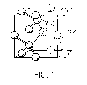
[0004] FIG. 1 illustrates one orientation of an NV center in a diamond
lattice.
[0005] FIG. 1 illustrates one orientation of an NV center in a diamond
lattice.
[0006] FIG. 2 is an energy level diagram showing energy levels of spin
states for the NV
center.
[0007] FIG. 3 is a schematic illustrating an NV center magnetic sensor
system.
[0008] FIG. 4 is a graph illustrating a fluorescence as a function of an
applied RF frequency
of an NV center along a given direction for a zero magnetic field.
[0009] FIG. 5 is a graph illustrating the fluorescence as a function of an
applied RF
frequency for four different NV center orientations for a non-zero magnetic
field.
4
CA 02974688 2017-07-21
WO 2016/118791 PCT/US2016/014403
[0010] FIG. 6 is a schematic diagram illustrating a magnetic field
detection system according
to an embodiment of the present invention.
[0011] FIG. 7 is a graph illustrating a fluorescence as a function of an
applied RF frequency
for an NV center orientation in a non-zero magnetic field and a gradient of
the fluorescence as a
function of the applied RF frequency.
[0012] FIG. 8 is an energy level diagram showing a hyperfine structure of
spin states for the
NV center.
[0013] FIG. 9 is a graph illustrating a fluorescence as a function of an
applied RF frequency
for an NV center orientation in a non-zero magnetic field with hyperfine
detection and a gradient
of the fluorescence as a function of the applied RF frequency.
[0014] FIG. 10 is an overview of a reflector with a diamond having nitrogen
vacancies.
[0015] FIG. 11 is a side view of an ellipsoidal reflector with a diamond
having nitrogen
vacancies and a photo detector.
[0016] FIG. 12 is a side view of an ellipsoidal diamond having nitrogen
vacancies and a
photo detector.
[0017] FIG. 13 is a side view of a parabolic reflector with a diamond
having nitrogen
vacancies and a photo detector.
[0018] FIG. 14 is a side view of a parabolic diamond having nitrogen
vacancies and a photo
detector.
[0019] FIG. 15 is a side view of a parabolic reflector with a flat diamond
having nitrogen
vacancies inserted parallel to a major axis of the parabolic reflector and a
photo detector.
[0020] FIG. 16 is a side view of a parabolic reflector with a flat diamond
having nitrogen
vacancies inserted parallel to a minor axis of the parabolic reflector and a
photo detector.
CA 02974688 2017-07-21
WO 2016/118791 PCT/US2016/014403
[0021] FIG. 17 is a side view of a sensor assembly with a parabolic diamond
having nitrogen
vacancies and a photo detector.
[0022] FIG. 18 is a side view of a sensor assembly with a waveguide
provided within a
parabolic reflector.
[0023] FIG. 19 is a process diagram for a method for constructing a DNV
sensor.
[0024] FIG. 20 is another process diagram for a method for constructing a
DNV sensor.
[0025] FIG. 21 is a block diagram depicting a general architecture for a
computer system that
may be employed to implement various elements of the systems and methods
described and
illustrated herein.
[0026] FIG. 22 is a schematic illustrating a position sensor system
according to one
embodiment.
[0027] FIG. 23 is a schematic illustrating a position sensor system
including a rotary position
encoder.
[0028] FIG. 24 is a schematic illustrating a top down view of a rotary
position encoder.
[0029] FIG. 25 is a schematic illustrating a position sensor system
including a linear position
encoder.
[0030] FIG. 26 is a schematic illustrating a magnetic element arrangement
of a position
encoder according to one embodiment.
[0031] FIG. 27 is a schematic illustrating a magnetic element arrangement
of a position
encoder according to another embodiment.
[0032] FIG. 28 is a schematic illustrating a magnetic element arrangement
of a position
encoder according to another embodiment.
6
CA 02974688 2017-07-21
WO 2016/118791 PCT/US2016/014403
[0033] FIG. 29 is a schematic illustrating the relationship of a position
sensor head and the
magnetic elements of a position encoder.
[0034] FIG. 30 is a graph of measured magnetic field intensity attributable
to magnetic
elements of a position encoder for a first magnetic field sensor and a second
magnetic field
sensor of a position sensor head.
[0035] FIG. 31 is a flow chart illustrating the process of determining a
position utilizing a
position sensor system according to one embodiment.
[0036] FIGs. 32A and 32B are graphs illustrating the frequency response of
a DNV sensor in
accordance with an illustrative embodiment.
[0037] FIGs. 33A is a diagram of NV center spin states in accordance with
an illustrative
embodiment.
[0038] FIG. 33B is a graph illustrating the frequency response of a DNV
sensor in response
to a changed magnetic field in accordance with an illustrative embodiment.
[0039] FIG. 34 is a block diagram of a magnetic communication system in
accordance with
an illustrative embodiment.
[0040] FIGs. 35A and 35B show the strength of a magnetic field versus
frequency in
accordance with an illustrative embodiment.
[0041] FIG. 36 is a block diagram of a computing device in accordance with
an illustrative
embodiment.
[0042] FIG. 37 is graphs illustrating the fluorescence as a function of
applied RF frequency
of four different NV center orientations for a magnetic field applied in
opposite directions to the
NV center diamond material.
[0043] FIG. 38 is a graph illustrating the fluorescence intensity as a
function of time for a
NV center diamond material with a pulsed RF excitation.
7
CA 02974688 2017-07-21
WO 2016/118791 PCT/US2016/014403
[0044] FIG. 39 is a graph illustrating the fluorescence as a function of
applied RF frequency
of four different NV center orientations for a magnetic field applied in
opposite directions to the
NV center diamond material, with a Lorentzian pair being identified in the
graph.
[0045] FIG. 40 is a graph illustrating the fluorescence intensity as a
function of time for a
NV center diamond material for a pulse of RF excitation.
[0046] FIG. 41 is a graph illustrating the normalized fluorescence
intensity as a function of
time for a pair of Lorentzian peaks of a NV center diamond material.
[0047] FIG. 42 is a graph illustrating the time to 60% of the equilibrium
fluorescence as a
function of RF frequency for a negative and positive magnetic bias field
applied to a NV center
diamond material.
[0048] FIGs. 43A and 43B are diagrams illustrating hydrophone systems in
accordance with
illustrative embodiments.
[0049] FIG. 44 illustrates a low altitude flying object in accordance with
some illustrative
implementations.
[0050] FIG. 45A illustrates a ratio of signal strength of two magnetic
sensors, A and B,
attached to wings of the UAS as a function of distance, x, from a center line
of a power in
accordance with some illustrative implementations.
[0051] FIG. 45B illustrates a composite magnetic field (B-filed) in
accordance with some
illustrative implementations.
[0052] FIG. 46 illustrates a high-level block diagram of an example UAS
navigation system
in accordance with some illustrative implementations.
[0053] FIG. 47 illustrates an example of a power line infrastructure.
[0054] FIGs. 48A and 48B illustrate examples of magnetic field distribution
for overhead
power lines and underground power cables.
8
CA 02974688 2017-07-21
WO 2016/118791 PCT/US2016/014403
[0055] FIG. 49 illustrates examples of magnetic field strength of power
lines as a function of
distance from the centerline.
[0056] FIG. 50 illustrates an example of a UAS equipped with DNV sensors in
accordance
with some illustrative implementations.
[0057] FIG. 51 illustrates a plot of a measured differential magnetic field
sensed by the DNV
sensors when in close proximity of the power lines in accordance with some
illustrative
implementations.
[0058] FIG. 52 illustrates an example of a measured magnetic field
distribution for normal
power lines and power lines with anomalies according to some implementations.
[0059] FIG. 53 is a depiction of the energy levels of an NV center which
contribute to the
Hamiltonian thereof.
[0060] FIG. 54 is a graph illustrating fluorescence as a function of
applied RF frequency of
an NV center for a zero external magnetic bias field.
[0061] FIG. 55 is a graph illustrating fluorescence as a function of
applied RF frequency of a
high quality NV center sample for an applied external magnetic bias field.
[0062] FIG. 56 is a graph illustrating fluorescence as a function of
applied RF frequency of a
low quality NV center sample for an applied external magnetic bias field.
[0063] FIG. 57 is a signal flow block diagram of an open loop processing of
the total
incident magnetic field on the NV center magnetic sensor system.
[0064] FIG. 58 is a signal flow block diagram of a closed loop processing
of the total
incident magnetic field on the NV center magnetic sensor system.
[0065] FIG. 59 is a flowchart showing a method of the closed loop
processing of FIG. 58.
[0066] FIG. 60 is a schematic diagram illustrating a magnetic field
detection system
according to an embodiment of the present invention.
9
CA 02974688 2017-07-21
WO 2016/118791 PCT/US2016/014403
[0067] FIG. 61 is a schematic illustrating a Ramsey sequence of optical
excitation pulses and
RF excitation pulses according to an operation of the system of FIG. 60.
[0068] FIG. 62A is a free induction decay curve where a free precession
time T is varied
using the Ramsey sequence of FIG. 61.
[0069] FIG. 62B is a magnetometry curve where a RF detuning frequency A is
varied using
the Ramsey sequence of FIG. 61.
[0070] FIG. 63A is a free induction decay surface plot where both the free
precession time T
and the RF detuning frequency A are varied using the Ramsey sequence of
FIG.61.
[0071] FIG. 63B is a plot showing a gradient of the free induction decay
surface plot of FIG.
63B.
[0072] FIG. 64 is a schematic illustrating a Rabi sequence of optical
excitation pulses and RF
pulses according to an operation of the system of FIG. 60.
[0073] FIG. 65 is a comparison of graphs showing resonant Rabi frequencies
according to a
power of RF excitation applied to the system of FIG. 60.
[0074] FIG. 66 is a graph showing raw pulse data collected during an
operation of the system
of FIG. 60.
[0075] FIG. 67 is a schematic illustrating a portion of a DNV sensor with a
coil assembly in
accordance with some illustrative implementations.
[0076] FIG. 68 is a schematic illustrating a cross section of a portion of
a DNV sensor with a
coil assembly in accordance with some illustrative implementations.
[0077] FIGS. 69A and 69B are schematics illustrating a coil assembly in
accordance with
some illustrative implementations.
[0078] FIG. 70 is a cross section illustrating a coil assembly in
accordance with some
illustrative implementations.
CA 02974688 2017-07-21
WO 2016/118791 PCT/US2016/014403
[0079] FIG. 71 is a schematic illustrating a side element of a coil
assembly in accordance
with some illustrative implementations.
[0080] FIG. 72 is a schematic illustrating a top or bottom element of a
coil assembly in
accordance with some illustrative implementations.
[0081] FIG. 73 is a schematic illustrating a center mounting block of a
coil assembly in
accordance with some illustrative implementations.
[0082] FIG. 74 is a cross section illustrating of a portion of a DNV sensor
with a coil
assembly in accordance with some illustrative implementations.
[0083] FIG. 75 is a schematic illustrating a coil assembly in accordance
with some
illustrative implementations.
[0084] FIG. 76 is a schematic illustrating a cross section of a coil
assembly in accordance
with some illustrative implementations.
[0085] FIG. 77 is a schematic illustrating a side element of a coil
assembly in accordance
with some illustrative implementations.
[0086] FIG. 78 is a schematic illustrating a portion of a DNV sensor with a
coil assembly in
accordance with some illustrative implementations.
[0087] FIG. 79 is a schematic illustrating a cross section of a portion of
a DNV sensor with a
coil assembly in accordance with some illustrative implementations.
[0088] FIG. 80 is a schematic illustrating a cross section of a portion of
a DNV sensor with a
coil assembly in accordance with some illustrative implementations.
[0089] FIG. 81 is a schematic illustrating a coil assembly in accordance
with some
illustrative implementations.
[0090] FIG. 82 is a schematic illustrating a cross section of a coil
assembly in accordance
with some illustrative implementations.
11
CA 02974688 2017-07-21
WO 2016/118791 PCT/US2016/014403
[0091] FIG. 83 is a schematic illustrating a side element of a coil
assembly in accordance
with some illustrative implementations.
[0092] FIGs. 84A and 84B are schematics illustrating top and bottom
elements of a coil
assembly in accordance with some illustrative implementations.
[0093] FIG. 85 illustrates a geomagnetic noise model compared with
empirical noise data.
[0094] FIG. 86 is a graph illustrating a signal of interest due to a
distortion in the magnetic
field in the Z-direction as measured by a single magnetic sensor.
[0095] FIGs. 87A-87C are graphs illustrating the signal of interest due to
a distortion in the
magnetic field in the Z-direction as measured by a two-dimensional magnetic
sensor array for
times of 1100, 1115 and 1120 seconds, respectively.
[0096] FIG. 88 is a schematic illustrating a magnetic sensor array system
according to an
embodiment of the invention.
[0097] FIGs. 89A and 89B respectively illustrate a common coordinate system
and a
coordinate system corresponding to one of the magnetic sensors of the array.
[0098] FIG. 90 is a schematic illustrates an orientation sensor attached to
a magnetic field
sensor according to an embodiment of the invention.
[0099] FIGs. 91A-91C are graphs illustrating a magnetic field measurement
component
along the X-direction, Y-direction and Z-direction, respectively, at a time of
500 seconds for a
two-dimensional array of magnetic field sensors in the case of a single
unmanned underwater
vehicle (UUV).
[00100] FIGs. 91D-91F are graphs illustrating a magnetic field measurement
component
along the X-direction, Y-direction and Z-direction, respectively, at a time of
1000 seconds for a
two-dimensional array of magnetic field sensors in the case of a single UUV.
12
CA 02974688 2017-07-21
WO 2016/118791 PCT/US2016/014403
[00101] FIGs. 91G-91I are graphs illustrating a magnetic field measurement
component along
the X-direction, Y-direction and Z-direction, respectively, at a time of 1500
seconds for a two-
dimensional array of magnetic field sensors in the case of a single UUV.
[00102] FIGs. 92A-92C are graphs illustrating a magnetic field measurement
component
along the X-direction, Y-direction and Z-direction, respectively, at a time of
500 seconds for a
two-dimensional array of magnetic field sensors in the case of two UUVs.
[00103] FIGs. 92D-92F are graphs illustrating a magnetic field measurement
component
along the X-direction, Y-direction and Z-direction, respectively, at a time of
1000 seconds for a
two-dimensional array of magnetic field sensors in the case of two UUVs.
[00104] FIGs. 92G-92I are graphs illustrating a magnetic field measurement
component along
the X-direction, Y-direction and Z-direction, respectively, at a time of 1500
seconds for a two-
dimensional array of magnetic field sensors in the case of two UUVs.
[00105] FIG. 93A is a graph illustrating the X-direction component of the
noise free and
measured magnetic fields as a function of time for a single magnetic field
sensor measurement.
[00106] FIG. 93B is a graph illustrating the noise free and reconstructed X-
direction
component of the magnetic field as a function of time for a single magnetic
field sensor
measurement as a function of time, where the noise has been removed by a
median subtraction
algorithm.
[00107] FIG. 93C is a graph illustrating the difference in the noise free and
reconstructed X-
direction component of the magnetic fields of FIG. 93B.
[00108] FIGs. 94A-94C are graphs illustrating the magnetic field for an array
of sensors
including the signal of interest in the X-direction for the array at times of
500, 1000 and 1500
seconds, respectively.
13
CA 02974688 2017-07-21
WO 2016/118791 PCT/US2016/014403
[00109] FIGs. 95A-95C are graphs illustrating, in the X-direction, a region of
interest and a
expanded region of interest as a results of set closing and convex hulling, at
respective times of
500, 1000 and 1500 seconds for a single UUV.
[00110] FIGs. 96A-96C are graphs illustrating a fit to a plane of the X-
direction component of
magnetic field measurement data with the region of interest data removed for a
two-dimensional
array of magnetic field sensors at times of 500, 1000 and 1500 seconds,
respectively.
[00111] FIG. 97A is a graph illustrating the X-direction component of noise
free and
measured magnetic fields as a function of time for a single magnetic field
sensor measurement.
[00112] FIG. 97B is a graph illustrating the noise free and reconstructed X-
direction
component of the magnetic field as a function of time for a single magnetic
field sensor
measurement as a function of time, where the noise has been removed using
noise fit to a plane.
[00113] FIG. 97C is a graph illustrating the difference in the noise free and
reconstructed X-
direction component of the magnetic field of FIG. 97B.
[00114] FIGs. 98A-98C are graphs illustrating a fit to a quadratic spline of
the X-direction
component of magnetic field measurement data with the region of interest data
removed for a
two-dimensional array of magnetic field sensors at times of 500, 1000 and 1500
seconds,
respectively.
[00115] FIG. 99A is a graph illustrating the X-direction component of noise
free and
measured magnetic fields as a function of time for a single magnetic field
sensor measurement.
[00116] FIG. 99B is a graph illustrating the noise free and reconstructed X-
direction
component of the magnetic field as a function of time for a single magnetic
field sensor
measurement as a function of time, where the noise has been removed using
noise fit to a
quadratic spline.
[00117] FIG. 99C is a graph illustrating the difference in the noise free and
reconstructed X-
direction component of the magnetic field of FIG. 99B.
14
CA 02974688 2017-07-21
WO 2016/118791 PCT/US2016/014403
[00118] FIGs. 100A-100C are graphs illustrating, in the X-direction, a region
of interest and a
expanded region of interest as a results of set closing and convex hulling, at
respective times of
500, 1000, and 1500 seconds for two UUVs.
[00119] FIGs. 101A-101C are graphs illustrating a fit to a quadratic spline
of the X-direction
component of magnetic field measurement data with the region of interest data
removed for a
two-dimensional array of magnetic field sensors at times of 500, 1000 and 1500
seconds,
respectively, for two UUVs.
[00120] FIG. 102A is a graph illustrating X-direction component of noise free
and measured
magnetic fields as a function of time for a single magnetic field sensor
measurement for two
UUVs.
[00121] FIG. 102B is a graph illustrating the noise free and reconstructed X-
direction
component of the magnetic field as a function of time for a single magnetic
field sensor
measurement as a function of time, where the noise has been removed using
noise fit to a
quadratic spline.
[00122] FIG. 102C is a graph illustrating the difference in the noise free and
reconstructed X-
direction component of the magnetic field of FIG. 102B.
[00123] FIG. 103A is a top perspective view of a sensor assembly according to
an
embodiment of the invention.
[00124] FIG. 103B is a bottom perspective view of the sensor assembly of FIG.
103A.
[00125] FIG. 104A is a top perspective view of a diamond assembly of the
sensor assembly of
FIG. 103A.
[00126] FIG. 104B is a bottom perspective view of the diamond assembly of FIG.
104A.
[00127] FIG. 104C is a side view of an assembly substrate of the sensor
assembly of FIG.
104A.
CA 02974688 2017-07-21
WO 2016/118791 PCT/US2016/014403
[00128] FIG. 105 is a top view of the diamond assembly of FIG. 104A.
[00129] FIG. 106A and 106B are side views of diamond material with metal
layers illustrating
steps of forming a RF excitation source according to an embodiment.
[00130] FIG. 107A is a top view of the diamond assembly according to another
embodiment.
[00131] FIG. 107B is a side view of the diamond assembly if FIG. 107A.
[00132] FIG. 108 is a graphical diagram depicting NVO and NV- photon intensity
relative to
wavelength without fluorescence manipulation.
[00133] FIG. 109 is a graphical diagram for the indirect band gap for a
diamond having
nitrogen vacancies depicting a valence band and a conduction band on an energy
versus
momentum (E vs. k) plot and showing a zero phonon line, an optical drive for
exciting an
electron over the band gap, and the recombination of the electron from various
points of the
conduction band to generate photons.
[00134] FIG. 110 is a graphical diagram depicting NVO and NV- photon intensity
relative to
wavelength with fluorescence manipulation.
[00135] FIG. 111 is a process diagram for fluorescence manipulation of the
diamond having
nitrogen vacancies through phonon spectrum manipulation using an acoustic
driver.
[00136] FIG. 112 is a process diagram for determining an acoustic driving
frequency for
phonon spectrum manipulation.
[00137] FIG. 113A is a block diagram of a magnetometer with a light pipe in
accordance with
an illustrative embodiment.
[00138] FIGs. 113B and 113C are isometric views of a light pipe and a shield
in accordance
with illustrative embodiments.
[00139] FIG. 114 is a block diagram of a magnetometer with two light pipes in
accordance
with an illustrative embodiment.
16
CA 02974688 2017-07-21
WO 2016/118791 PCT/US2016/014403
[00140] FIG. 115 is a block diagram of a magnetometer with two light pipes in
accordance
with an illustrative embodiment.
[00141] FIG. 116 is a flow diagram of a method for measuring a magnetic field
in accordance
with an illustrative embodiment.
[00142] FIG. 117 is a block diagram of a magnetometer in accordance with an
illustrative
embodiment.
[00143] FIG. 118 is an exploded view of a magnetometer in accordance with an
illustrative
embodiment.
[00144] FIG. 119 is a flow diagram of a method for detecting a magnetic field
in accordance
with an illustrative embodiment.
[00145] FIG 120 is a schematic illustrating a portion of a DNV sensor with a
dual RF
arrangement in accordance with some illustrative implementations.
[00146] FIG. 121 is a view of an enclosed DNV sensor with a dual RF
arrangement in
accordance with some illustrative implementations.
[00147] FIGs. 122A and 122B are schematics of an assembly portion of a DNV
sensor with a
dual RF arrangement in accordance with some illustrative implementations.
[00148] FIG. 123 is a cross-section of a portion of a DNV sensor with a dual
RF arrangement
in accordance with some illustrative implementations.
[00149] FIG. 124 is a schematic illustrating a DNV sensor with a dual RF
arrangement in
accordance with some illustrative implementations.
[00150] FIG. 125 is a cross-section of a DNV sensor with a dual RF arrangement
in
accordance with some illustrative implementations.
[00151] FIG. 126 is a schematic illustrating a DNV sensor with a dual RF
arrangement and
laser mounting in accordance with some illustrative implementations.
17
CA 02974688 2017-07-21
WO 2016/118791 PCT/US2016/014403
[00152] FIG. 127 is a cross-section of a DNV sensor with a dual RF arrangement
and laser
mounting in accordance with some illustrative implementations.
[00153] FIGs. 128A and 128B are schematics of an assembly portion of a DNV
sensor with a
dual RF arrangement in accordance with some illustrative implementations.
[00154] FIGs. 129A and 129B are schematics of an assembly portion of a DNV
sensor with a
dual RF arrangement in accordance with some illustrative implementations.
[00155] FIG. 130 is a block diagram of an overview of a single-cycle
synthesis, control, and
acquisition system for a diamond nitrogen vacancy sensor.
[00156] FIG. 131 is a block circuit diagram of the single-cycle control,
synthesis, and
acquisition processor for a diamond nitrogen vacancy sensor of FIG. 130.
[00157] FIG. 132A is a block circuit diagram of the host interface of FIG.
131.
[00158] FIG. 132B is a block circuit diagram of the program counter of FIG.
131.
[00159] FIG. 132C is a block circuit diagram of the program memory of FIG.
131.
[00160] FIG. 132D is a block circuit diagram of a first portion of the jump
control with delay
of FIG. 131.
[00161] FIG. 132E is a block circuit diagram of a second portion of the jump
control FIG.
131.
[00162] FIG. 132F is a block circuit diagram of the RF waveform generator of
FIG. 131.
[00163] FIG. 132G is a block circuit diagram of the digital control of FIG.
131.
[00164] FIG. 132H is a block circuit diagram of the acquisition processor of
FIG. 131.
[00165] FIG. 133A is a unit cell diagram of the crystal structure of a diamond
lattice having a
standard orientation.
18
CA 02974688 2017-07-21
WO 2016/118791 PCT/US2016/014403
[00166] FIG. 133B is a unit cell diagram of the crystal structure of a diamond
lattice having
an unknown orientation.
[00167] FIG. 134 is a schematic diagram illustrating a step in a method for
determining the
unknown orientation of the diamond lattice of FIG. 133B.
[00168] FIG. 135 is a flowchart illustrating a sign recovery method for the
method for
determining the unknown orientation of the diamond lattice of FIG. 133B.
[00169] FIG. 136 is a schematic diagram illustrating a step in the method for
determining the
unknown orientation of the diamond lattice of FIG. 133B.
[00170] FIG. 137 is a flowchart illustrating a method for recovering a three-
dimensional
magnetic field on the NV center magnetic sensor system.
[00171] FIG. 138 is an overview diagram of a diamond of a DNV sensor with a
low pass filter
and a high pass filter.
[00172] FIG. 139 is graphical diagram of an example signal detected with a DNV
sensor that
includes a test signal without filtering.
[00173] FIG. 140 is an overview diagram of a diamond of a DNV sensor with a
low pass filter
and showing a magnetic field of the environment, a change in the magnetic
field of the
environment, and an induced magnetic field by the low pass filter to filter
high frequency
signals.
[00174] FIG. 141 is another overview diagram of a diamond of a DNV sensor with
two low
pass filters arranged for spatial attenuation.
[00175] FIG. 142 is an overview diagram of a diamond of a DNV sensor relative
to a
diamagnetic material and showing alignment of the poles of the diamagnetic
material relative to
the induced magnetic field.
19
CA 02974688 2017-07-21
WO 2016/118791 PCT/US2016/014403
[00176] FIG. 143 is a graphical diagram of magnetism in a diamagnetic material
relative to
the applied magnetic field.
[00177] FIG. 144 is a process diagram for modifying a filtering frequency of a
low pass filter
for a DNV sensor based on a detected magnetic field.
[00178] FIG. 145 is a process diagram for modifying an orientation of a DNV
sensor with a
low pass filter based on a detected magnetic field.
[00179] FIG. 146 illustrates a low altitude flying object in accordance with
some illustrative
implementations.
[00180] FIG. 147 illustrates a magnetic field detector in accordance with some
illustrative
implementations.
[00181] FIGs. 148A and 148B illustrate a portion of a detector array in
accordance with some
illustrative implementations.
[00182] FIG. 149 is a schematic illustrating a hydrophone in accordance with
some illustrative
implementations.
[00183] FIG. 150 is a schematic illustrating a portion of a vehicle with a
hydrophone in
accordance with some illustrative implementations.
[00184] FIG. 151 is a schematic illustrating a portion of a vehicle with a
hydrophone with a
containing membrane in accordance with some illustrative implementations.
[00185] FIG. 152 is a schematic illustrating a portion of a vehicle with a
hydrophone in
accordance with some illustrative implementations.
[00186] FIG. 153 is a schematic illustrating a portion of a vehicle with a
hydrophone with a
containing membrane in accordance with some illustrative implementations.
[00187] FIG. 154 is a schematic illustrating a system for AC magnetic vector
anomaly
detection according to an embodiment of the invention.
CA 02974688 2017-07-21
WO 2016/118791 PCT/US2016/014403
[00188] FIG. 155 is a schematic illustrating a sequence of optical excitation
pulses and RF
pulses according to the operation of the system of FIG. 156.
[00189] FIG. 156 is a graph illustrating the fluorescence signal of NV diamond
material as a
function of RF excitation frequency over an range of RF frequencies according
to an
embodiment of the invention.
[00190] FIG. 157A illustrates a matched-filtered first correlated code for
the magnetic field
component along three different diamond lattice directions corresponding to
the magnetic field
provided by a first magnetic field generator according to an embodiment of the
invention.
[00191] FIG. 157B illustrates a matched-filtered first correlated code for
the magnetic field
component along three different diamond lattice directions corresponding to
the magnetic field
provided by a second magnetic field generator according to an embodiment of
the invention.
[00192] FIG. 158 illustrates reconstructed magnetic field vectors for two
different correlated
codes in the case where a ferrous object and no object are disposed in
relation to a magnetic field
generator and NV diamond material, according to an embodiment of the
invention.
[00193] FIGs. 159A and 159B are block diagrams of a system for detecting
deformities in a
material in accordance with an illustrative embodiment.
[00194] FIGs. 160 illustrates current paths through a conductor with a
deformity in
accordance with an illustrative embodiment.
[00195] FIGs. 161 is a flow diagram of a method for detecting deformities in
accordance with
an illustrative embodiment.
[00196] FIG. 162 is a block diagram of a vehicular system in accordance with
an illustrative
embodiment.
[00197] FIG. 163 is a flow chart of a method for charging a power source in
accordance with
an illustrative embodiment.
21
CA 02974688 2017-07-21
WO 2016/118791 PCT/US2016/014403
[00198] FIG. 164 is a graph of the strength of a magnetic field versus
distance from the
conductor in accordance with an illustrative embodiment.
[00199] FIGs. 165A and 165B are block diagrams of a system for detecting
deformities in
transmission lines in accordance with an illustrative embodiment.
[00200] FIG. 166 illustrates current paths through a transmission line with a
deformity in
accordance with an illustrative embodiment.
[00201] FIG. 167 illustrates power transmission line sag between transmission
towers in
accordance with an illustrative embodiment.
[00202] FIG. 168 illustrates vector measurements indicating power transmission
line sag in
accordance with an illustrative embodiment.
[00203] FIG. 169 illustrates vector measurements along a path between adjacent
towers in
accordance with an illustrative embodiment.
DETAILED DESCRIPTION
[00204] HYPERSENSITIVITY DETECTION OF MAGNETIC FIELD
[00205] Aspects of the disclosure relates to apparatuses and methods for
elucidating hyperfine
transition responses to determine an external magnetic field acting on a
magnetic detection
system. The hyperfine transition responses exhibit a steeper gradient than the
gradient of
aggregate Lorentzian responses measured in conventional systems, which can be
up to three
orders of magnitude larger. The steeper gradient exhibited by the hyperfine
transition responses
thus allow for a comparable increase in measurement sensitivity in a magnetic
detection system.
By utilizing the largest gradient of the hyperfine responses for measuring
purposes, external
magnetic fields may be detected more accurately, especially low magnitude
and/or rapidly
changing fields.
[00206] The NV Center, Its Electronic Structure, and Optical and RF
Interaction
22
CA 02974688 2017-07-21
WO 2016/118791 PCT/US2016/014403
[00207] The NV center in a diamond comprises a substitutional nitrogen atom in
a lattice site
adjacent a carbon vacancy as shown in FIG. 1. The NV center may have four
orientations, each
corresponding to a different crystallographic orientation of the diamond
lattice.
[00208] The NV center may exist in a neutral charge state or a negative charge
state.
Conventionally, the neutral charge state uses the nomenclature NV , while the
negative charge
state uses the nomenclature NV, which is adopted in this description.
[00209] The NV center has a number of electrons, including three unpaired
electrons, each
one from the vacancy to a respective of the three carbon atoms adjacent to the
vacancy, and a
pair of electrons between the nitrogen and the vacancy. The NV center, which
is in the
negatively charged state, also includes an extra electron.
[00210] The NV center has rotational symmetry, and as shown in FIG. 2, has a
ground state,
which is a spin triplet with 3A2 symmetry with one spin state ms = 0, and two
further spin states
ms = +1, and ms = -1. In the absence of an external magnetic field, the ms =
1 energy levels are
offset from the ms = 0 due to spin-spin interactions, and the ms = 1 energy
levels are
degenerate, i.e., they have the same energy. The ms = 0 spin state energy
level is split from the
ms = 1 energy levels by an energy of 2.87 GHz for a zero external magnetic
field.
[00211] Introducing an external magnetic field with a component along the NV
axis lifts the
degeneracy of the ms = 1 energy levels, splitting the energy levels ms = 1
by an amount
2gpBBz, where g is the g-factor, [LB is the Bohr magneton, and Bz is the
component of the
external magnetic field along the NV axis. This relationship is correct to a
first order and
inclusion of higher order corrections is straightforward matter and will not
affect the
computational and logic steps in the systems and methods described below.
[00212] The NV center electronic structure further includes an excited triplet
state 3E with
corresponding ms = 0 and ms = 1 spin states. The optical transitions between
the ground state
3A2 and the excited triplet 3E are predominantly spin conserving, meaning that
the optical
transitions are between initial and final states that have the same spin. For
a direct transition
between the excited triplet 3E and the ground state 3A2, a photon of red light
is emitted with a
23
CA 02974688 2017-07-21
WO 2016/118791 PCT/US2016/014403
photon energy corresponding to the energy difference between the energy levels
of the
transitions.
[00213] There is, however, an alternative non-radiative decay route from the
triplet 3E to the
ground state 3A2 via intermediate electron states, which are thought to be
intermediate singlet
states A, E with intermediate energy levels. Significantly, the transition
rate from the ms = 1
spin states of the excited triplet 3E to the intermediate energy levels is
significantly greater than
the transition rate from the ms = 0 spin state of the excited triplet 3E to
the intermediate energy
levels. The transition from the singlet states A, E to the ground state
triplet 3A2 predominantly
decays to the ms = 0 spin state over the ms = 1 spins states. These features
of the decay from
the excited triplet 3E state via the intermediate singlet states A, E to the
ground state triplet 3A2
allows that if optical excitation is provided to the system, the optical
excitation will eventually
pump the NV center into the ms = 0 spin state of the ground state 3A2. In this
way, the
population of the ms = 0 spin state of the ground state 3A2 may be "reset" to
a maximum
polarization determined by the decay rates from the triplet 3E to the
intermediate singlet states.
[00214] Another feature of the decay is that the fluorescence intensity due to
optically
stimulating the excited triplet 3E state is less for the ms = 1 states than
for the ms = 0 spin state.
This is so because the decay via the intermediate states does not result in a
photon emitted in the
fluorescence band, and because of the greater probability that the ms = 1
states of the excited
triplet 3E state will decay via the non-radiative decay path. The lower
fluorescence intensity for
the ms = 1 states than for the ms = 0 spin state allows the fluorescence
intensity to be used to
determine the spin state. As the population of the ms = 1 states increases
relative to the ms = 0
spin, the overall fluorescence intensity will be reduced.
[00215] The NV Center, or Magneto-Optical Defect Center, Magnetic Sensor
System
[00216] FIG. 3 is a schematic diagram illustrating a conventional NV center
magnetic sensor
system 300 that uses fluorescence intensity to distinguish the ms = 1 states,
and to measure the
magnetic field based on the energy difference between the ms = +1 state and
the ms = -1 state.
The system 300 includes an optical excitation source 310, which directs
optical excitation to an
NV diamond material 320 with NV centers. The system further includes an RF
excitation source
24
CA 02974688 2017-07-21
WO 2016/118791 PCT/US2016/014403
330, which provides RF radiation to the NV diamond material 320. Light from
the NV diamond
may be directed through an optical filter 350 to an optical detector 340.
[00217] The RF excitation source 330 may be a microwave coil, for example. The
RF
excitation source 330, when emitting RF radiation with a photon energy
resonant with the
transition energy between ground ms = 0 spin state and the ms = +1 spin state,
excites a transition
between those spin states. For such a resonance, the spin state cycles between
ground ms = 0
spin state and the ms = +1 spin state, reducing the population in the ms = 0
spin state and
reducing the overall fluorescence at resonances. Similarly, resonance occurs
between the ms = 0
spin state and the ms = -1 spin state of the ground state when the photon
energy of the RF
radiation emitted by the RF excitation source is the difference in energies of
the ms = 0 spin state
and the ms = -1 spin state, or between the ms = 0 spin state and the ms = +1
spin state, there is a
decrease in the fluorescence intensity.
[00218] The optical excitation source 310 may be a laser or a light
emitting diode, for
example, which emits light in the green, for example. The optical excitation
source 310 induces
fluorescence in the red, which corresponds to an electronic transition from
the excited state to the
ground state. Light from the NV diamond material 320 is directed through the
optical filter 350
to filter out light in the excitation band (in the green, for example), and to
pass light in the red
fluorescence band, which in turn is detected by the detector 340. The optical
excitation light
source 310, in addition to exciting fluorescence in the diamond material 320,
also serves to reset
the population of the ms = 0 spin state of the ground state 3A2 to a maximum
polarization, or
other desired polarization.
[00219] For continuous wave excitation, the optical excitation source 310
continuously pumps
the NV centers, and the RF excitation source 330 sweeps across a frequency
range that includes
the zero splitting (when the ms = 1 spin states have the same energy) energy
of 2.87 GHz. The
fluorescence for an RF sweep corresponding to a diamond material 320 with NV
centers aligned
along a single direction is shown in FIG. 4 for different magnetic field
components Bz along the
NV axis, where the energy splitting between the ms = -1 spin state and the ms
= +1 spin state
increases with Bz. Thus, the component Bz may be determined. Optical
excitation schemes
CA 02974688 2017-07-21
WO 2016/118791 PCT/US2016/014403
other than continuous wave excitation are contemplated, such as excitation
schemes involving
pulsed optical excitation, and pulsed RF excitation. Examples of pulsed
excitation schemes
include Ramsey pulse sequence, and spin echo pulse sequence.
[00220] In general, the diamond material 320 will have NV centers aligned
along directions of
four different orientation classes. FIG. 5 illustrates fluorescence as a
function of RF frequency
for the case where the diamond material 320 has NV centers aligned along
directions of four
different orientation classes. In this case, the component Bz along each of
the different
orientations may be determined. These results, along with the known
orientation of
crystallographic planes of a diamond lattice, allow not only the magnitude of
the external
magnetic field to be determined, but also the direction of the magnetic field.
[00221] While FIG. 3 illustrates an NV center magnetic sensor system 300 with
NV diamond
material 320 with a plurality of NV centers, in general, the magnetic sensor
system may instead
employ a different magneto-optical defect center material, with a plurality of
magneto-optical
defect centers. The electronic spin state energies of the magneto-optical
defect centers shift with
magnetic field, and the optical response, such as fluorescence, for the
different spin states is not
the same for all of the different spin states. In this way, the magnetic field
may be determined
based on optical excitation, and possibly RF excitation, in a corresponding
way to that described
above with NV diamond material.
[00222] FIG. 6 is a schematic diagram of a system 600 for a magnetic field
detection system
according to an embodiment of the present invention. The system 600 includes
an optical
excitation source 610, which directs optical excitation to an NV diamond
material 620 with NV
centers, or another magneto-optical defect center material with magneto-
optical defect centers.
An RF excitation source 630 provides RF radiation to the NV diamond material
620.
[00223] As shown in FIG. 6, a first magnetic field generator 670 generates a
magnetic field,
which is detected at the NV diamond material 620. The first magnetic field
generator 670 may
be a permanent magnet positioned relative to the NV diamond material 620,
which generates a
known, uniform magnetic field (e.g., a bias or control magnetic field) to
produce a desired
fluorescence intensity response from the NV diamond material 620. In some
embodiments, a
26
CA 02974688 2017-07-21
WO 2016/118791 PCT/US2016/014403
second magnetic field generator 675 may be provided and positioned relative to
the NV diamond
material 620 to provide an additional bias or control magnetic field. The
second magnetic field
generator 675 may be configured to generate magnetic fields with orthogonal
polarizations, for
example. In this regard, the second magnetic field generator 675 may include
one or more coils,
such as a Helmholtz coils. The coils may be configured to provide relatively
uniform magnetic
fields at the NV diamond material 620 and each may generate a magnetic field
having a direction
that is orthogonal to the direction of the magnetic field generated by the
other coils. For
example, in a particular embodiment, the second magnetic field generator 675
may include three
Helmholtz coils that are arranged to each generate a magnetic field having a
direction orthogonal
to the other direction of the magnetic field generated by the other two coils
resulting in a three-
axis magnetic field. In some embodiments, only the first magnetic field
generator 670 may be
provided to generate a bias or control magnetic field. Alternatively, only the
second magnetic
field generator 675 may be provided to generate the bias or control magnetic
field. In yet other
embodiments, the first and/or second magnetic field generators may be affixed
to a pivot
assembly (e.g., a gimbal assembly) that may be controlled to hold and position
the first and/or
second magnetic field generators to a predetermined and well-controlled set of
orientations,
thereby establishing the desired bias or control magnetic fields. In this
case, the controller 680
may be configured to control the pivot assembly having the first and/or second
magnetic field
generators to position and hold the first and/or second magnetic field
generators at the
predetermined orientation.
[00224] The system 600 further includes a controller 680 arranged to receive a
light detection
or optical signal from the optical detector 640 and to control the optical
excitation source 610,
the RF excitation source 630, and the second magnetic field generator 675. The
controller may
be a single controller, or multiple controllers. For a controller including
multiple controllers,
each of the controllers may perform different functions, such as controlling
different components
of the system 600. The second magnetic field generator 675 may be controlled
by the controller
680 via an amplifier 660, for example.
[00225] The RF excitation source 630 may be a microwave coil, for example. The
RF
excitation source 630 is controlled to emit RF radiation with a photon energy
resonant with the
27
CA 02974688 2017-07-21
WO 2016/118791 PCT/US2016/014403
transition energy between the ground ms = 0 spin state and the ms = 1 spin
states as discussed
above with respect to FIG. 3.
[00226] The optical excitation source 610 may be a laser or a light emitting
diode, for
example, which emits light in the green, for example. The optical excitation
source 610 induces
fluorescence in the red from the NV diamond material 620, where the
fluorescence corresponds
to an electronic transition from the excited state to the ground state. Light
from the NV diamond
material 620 is directed through the optical filter 650 to filter out light in
the excitation band (in
the green, for example), and to pass light in the red fluorescence band, which
in turn is detected
by the optical detector 640. The optical excitation light source 610, in
addition to exciting
fluorescence in the NV diamond material 620, also serves to reset the
population of the ms = 0
spin state of the ground state 3A2 to a maximum polarization, or other desired
polarization.
[00227] The controller 680 is arranged to receive a light detection signal
from the optical
detector 640 and to control the optical excitation source 610, the RF
excitation source 630, and
the second magnetic field generator 675. The controller may include a
processor 682 and a
memory 684, in order to control the operation of the optical excitation source
610, the RF
excitation source 630, and the second magnetic field generator 675. The memory
684, which
may include a nontransitory computer readable medium, may store instructions
to allow the
operation of the optical excitation source 610, the RF excitation source 630,
and the second
magnetic field generator 675 to be controlled. That is, the controller 680 may
be programmed to
provide control.
[00228] Detection of Magnetic Field Changes
[00229] As discussed above, the interaction of the NV centers with an external
magnetic field
results in an energy splitting between the ms = -1 spin state and the ms = +1
spin state that
increases with Bz as shown in FIG. 4, for example. The pair of frequency
responses (also known
as Lorentzian responses, profiles, or dips) due to the component of the
external magnetic field
along the given NV axis manifest as dips in intensity of the emitted red light
from the NV centers
as a function of RF carrier frequency. Accordingly, a pair of frequency
responses for each of the
four axes of the NV center diamond lattice result in an energy splitting
between the ms = -1 spin
28
CA 02974688 2017-07-21
WO 2016/118791 PCT/US2016/014403
state and the ms = +1 spin state that corresponds to the component of the
external magnetic field
along the axis for a total of eight Lorentzian profiles or dips, as shown in
FIG. 5. When a bias
magnetic field is applied to the NV diamond material (such as by the first
and/or second
magnetic field generators 670, 675 of FIG. 6), in addition to an unknown
external magnetic field
existing outside the system, the total incident magnetic field may thus be
expressed as B t(t) =
B bias (0 B õt(t), where B b ias (0 represents the bias magnetic field applied
to the NV
diamond material and B õt (t) represents the unknown external magnetic field.
This total
incident magnetic field creates equal and linearly proportional shifts in the
Lorentzian frequency
profiles for a given NV axis between the ms = -1 spin state and the ms = +1
spin state relative to
the starting carrier frequency (e.g., about 2.87 GHz).
[00230] Because the applied bias magnetic field B bias (t) is already known
and constant, a
change or shift in the total incident magnetic field B t(t) will be due to a
change in the external
magnetic field B õt(t). To detect a change in the total incident magnetic
field, the point of
greatest sensitivity in measuring such a change will occur at the point where
the frequency
response is at its largest slope. For example, as shown in FIG. 7, an
intensity response 1(t) as a
function of an RF applied frequency f (t) for a given NV axis due to a
magnetic field is shown in
dl (t)
the top graph. The change in intensity 1(t) relative to the change in RF
applied frequency, ¨df
is plotted against the RF applied frequency f (t) as shown in the bottom
graph. Point 25
represents the point of the greatest gradient of the Lorentzian dip 20. This
point gives the
greatest measurement sensitivity in detecting changes in the total incident
magnetic field as it
responds to the external magnetic field.
[00231] The Hyperfine Field
[00232] As discussed above and shown in the energy level diagram of FIG. 2,
the ground state
is split by about 2.87 GHz between the ms = 0 and ms = 1 spin states due to
their spin-spin
interactions. In addition, due to the presence of a magnetic field, the ms =
1 spin states split in
proportion to the magnetic field along the given axis of the NV center, which
manifests as the
four-pair Lorentzian frequency response shown in FIG. 5. However, a hyperfine
structure of the
NV center exists due to the hyperfine coupling between the electronic spin
states of the NV
29
CA 02974688 2017-07-21
WO 2016/118791 PCT/US2016/014403
center and the nitrogen nucleus, which results in further energy splitting of
the spin states. FIG.
8 shows the hyperfine structure of the ground state triplet 3A2 of the NV
center. Specifically,
coupling to the nitrogen nucleus "N further splits the ms = 1 spin states
into three hyperfine
transitions (labeled as m1 spin states), each having different resonances.
Accordingly, due to the
hyperfine split for each of the ms = 1 spin states, twenty-four different
frequency responses may
be produced (three level splits for each of the ms = 1 spin states for each
of the four NV center
orientations).
[00233] Each of the three hyperfine transitions manifest within the width of
one aggregate
Lorentzian dip. With proper detection, the hyperfine transitions may be
elucidated within a
given Lorentzian response. To detect such hyperfine transitions, in particular
embodiments, the
NV diamond material 620 exhibits a high purity (e.g., low existence of lattice
dislocations,
broken bonds, or other elements beyond "N) and does not have an excess
concentration of NV
centers. In addition, during operation of the system 600 in some embodiments,
the RF excitation
source 630 is operated on a low power setting in order to further resolve the
hyperfine responses.
In other embodiments, additional optical contrast for the hyperfine responses
may be
accomplished by increasing the concentration of NV negative-charge type
centers, increasing the
optical power density (e.g., in a range from about 20 to about 1000 mW/mm2),
and decreasing
the RF power to the lowest magnitude that permits a sufficient hyperfine
readout (e.g., about 1 to
about 10 W/mm2).
[00234] FIG. 9 shows an example of fluorescence intensity as a function of an
applied RF
frequency for an NV center with hyperfine detection. In the top graph, the
intensity response
1(0 as a function of an applied RF frequency f (t) for a given spin state
(e.g., ms = -1) along a
given axis of the NV center due to an external magnetic field is shown. In
addition, in the
dl(t)
bottom graph, the gradient ¨df plotted against the applied RF frequency f (t)
is shown. As seen
in the figure, the three hyperfine transitions 200a-200c constitute a complete
Lorentzian response
20 (e.g., corresponding to the Lorenztian response 20 in FIG. 7). The point of
maximum slope
may then be determined through the gradient of the fluorescence intensity as a
function of the
applied RF frequency, which occurs at the point 250 in FIG. 9. This point of
maximum slope
CA 02974688 2017-07-21
WO 2016/118791 PCT/US2016/014403
may then be tracked during the applied RF sweep to detect movement of the
point of maximum
slope along the frequency sweep. Like the point of maximum slope 25 for the
aggregate
Lorentzian response, the corresponding movement of the point 250 corresponds
to changes in the
total incident magnetic field B(t), which because of the known and constant
bias field Bbias(t),
allows for the detection of changes in the external magnetic field B õt (t) .
[00235] However, as compared to point 25, point 250 exhibits a larger gradient
than the
aggregate Lorentzian gradient described above with regard to FIG. 7. In some
embodiments, the
gradient of point 250 may be up to 1000 times larger than the aggregate
Lorentzian gradient of
point 25. Due to this, the point 250 and its corresponding movement may be
more easily
detected by the measurement system resulting in improved sensitivity,
especially in very low
magnitude and/or very rapidly changing magnetic fields.
[00236] IMPROVED LIGHT COLLECTION FROM DNV SENSORS
[00237] In some aspects of the present technology, methods and configurations
are disclosed
for an efficient collection of fluorescence (e.g., red light) emitted by the
nitrogen vacancies of a
diamond of a DNV sensor. In some implementations, the subject technology can
allow efficient
collection of the emitted light of the diamond of the DNV sensor with a
compact and low cost
reflector. The reflector can focus the emitted light of the diamond of the DNV
sensor to an
optical or photo detector that can increase the amount of light detected from
the diamond. In
some implementations, such a configuration may detect virtually all light
emitted by the diamond
of the DNV sensor. In some aspects, the reflector may be shaped as a parabola,
an ellipse, or
other shapes that can convey the light emitted from a source to a focal point
or focal area.
[00238] In some other implementations of the subject technology, the diamond
of the DNV
sensor may be machined or otherwise shaped to be a reflector itself That is,
the diamond with
nitrogen vacancies may be shaped to form a parabolic reflector, ellipsoidal
reflector or other
shapes that can convey the light emitted from the nitrogen vacancies to a
focal point or focal
area. For example, the reflector can be mostly parabolic or ellipsoidal such
that the light hits the
photo detector at a 90 degree angle with some margin of error, e.g., 2 to 10
degrees.
31
CA 02974688 2017-07-21
WO 2016/118791 PCT/US2016/014403
[00239] The nitrogen vacancies of the diamond will fluoresce in response to
excitation with
green light and will emit red light in random directions. Because the red
light measurements are
shot noise limited, collecting as much emitted light as possible is desirable.
In some current
collection approaches using large optics, the collection efficiencies were in
the range of 20%.
Some implementations use a large aperture lens mounted close to the diamond or
DNV sensor,
which limits light collection to a fraction of the light emitted by the
diamond or DNV sensor.
Other implementations use a flat diamond and a number of photo detectors
(e.g., four) positioned
at the edges of the flat diamond. This arrangement of photo detectors may be
able to capture
more of the emitted light conducted to edges of the flat diamond due to
internal reflection, but
increases the number of photo detectors required and may not capture light
emitted from the
faces of the flat diamond. The DNV sensors discussed herein provide an
alternative to increase
the collection efficiency.
[00240] FIG. 10 depicts an overview of an assembly 1000 with an example
diamond 1002
having nitrogen vacancies and a reflector 1004 positioned about the diamond
1002 for a DNV
light-collection apparatus. In the implementation shown, the reflector 1004 is
positioned about
the diamond 1002 to reflect a portion of the light emitted 1006 from the
diamond 1002. The
reflector 1004 is an elliptical or ellipsoidal reflector with the diamond 1002
positioned within a
portion of the reflector 1004. In other implementations, as discussed in
further detail herein, the
reflector 1004 may be parabolic or any other geometric configuration to
reflect light emitted
from the diamond 1002. In some implementations, the reflector 1004 may be a
monolithic
reflector, a hollow reflector, or any other type of reflector to reflect light
emitted from the
diamond 1002. In the implementation shown, the diamond 1002 is positioned at a
focus 1008 of
the reflector 1004. Thus, when light 1006 is emitted from the diamond 1002,
the light is reflected
by the reflector 1004 toward another focus of the reflector 1004. As will be
discussed in further
detail herein, a photo detector may be positioned at the second focus to
collect the reflected light.
[00241] FIG. 11 depicts an assembly 1100 with an example diamond 1102 having
nitrogen
vacancies and an ellipsoidal reflector 1104 positioned about the diamond 1102
for a DNV light-
collection apparatus. In some implementations, the ellipsoidal reflector 1104
can be a single
monolithic component that can be considered to be divided into two portions,
such as a reflector
32
CA 02974688 2017-07-21
WO 2016/118791 PCT/US2016/014403
portion 1106 and a concentrator portion 1108. In other implementations, the
ellipsoidal reflector
1104 may be divided into two components, such as the reflector portion 1106
and the
concentrator portion 1108 that are coupled and/or otherwise positioned
relative to each other. For
instance, the reflector portion 1106 and the concentrator portion 1108 may be
separate parabolic
components that can be combined to form the ellipsoidal reflector 1104. In
still further
configurations, the ellipsoidal reflector 1104 may be composed of more than
two components
and can be coupled or otherwise positioned to form the ellipsoidal reflector
1104.
[00242] The diamond 1102 is positioned at a first focus of the ellipsoidal
reflector 1104 for
the reflector portion 1106. In some implementations, the diamond 1102 is
positioned at the first
focus using a mount for the diamond 1102. In other implementations, the
diamond 1102 is
positioned at the first focus using a borehole through the ellipsoidal
reflector 1104. The borehole
may be backfilled to seal the diamond 1102 in the ellipsoidal reflector 1104.
[00243] The ellipsoidal reflector 1104 may also include an opening to allow an
excitation
laser beam to excite the diamond 1102, such as a green excitation laser beam.
The opening may
be positioned at any location for the ellipsoidal reflector 1104. When the
diamond 1102 is
excited (e.g., by applying green light to the diamond 1102), then the
reflector portion 1106
reflects the red light emitted 1110 from the diamond 1102 towards the
concentrator portion 1108.
[00244] The concentrator portion 1108 directs the emitted light 1110 toward a
second focus of
the ellipsoidal reflector 1104. In the implementation shown, a photo detector
1120 is positioned
to receive and measure the light from the concentrator portion 1108. In some
implementations,
the photo detector 1120 is positioned at the second focus to receive the
redirected emitted light.
In some implementations the photo detector 1120 is coupled and/or sealed to a
portion of the
ellipsoidal reflector 1104, such as to the concentrator portion 1108. In some
implementations, the
opening may be adjacent or proximate to the photo detector 1120, such as
through the
concentrator portion 1108. In other implementations, the opening may be
opposite the photo
detector 1120, such as through the reflector portion 1106. In still further
configurations, the
opening may be at any other angle and/or orientation relative to the photo
detector 1120.
33
CA 02974688 2017-07-21
WO 2016/118791 PCT/US2016/014403
[00245] In some implementations, an optical filter, such as a red filter,
may be applied to
and/or positioned on the photo detector 1120 to filter out light except the
relevant red light of
interest. Thus, the ellipsoidal reflector 1104 is concatenated with a non-
focusing concentrator
that can capture the emitted light from a light source (e.g., from the
nitrogen vacancies of the
diamond of a DNV sensor) to a single photo detector. In some instances, the
loss of emitted light
can be limited to the light loss due to the mount for the diamond and/or the
small entrance for the
green stimulation laser beam.
[00246] The foregoing solution provides high light collection efficiency to
collect the light
emitted from the diamond 1102, while utilizing a reflector 1104 that may not
require high
precision refinements. Such a reflector 1104 may be a low cost solution to
increase the light
collection efficiency, such as using a reflective mirror component. In
addition, the shape of the
ellipsoidal reflector 1104 may separate the electronics of the photo detector
1120 from the
diamond 1102, which may decrease the magnetic interaction between the
electronics of the photo
detector 1120 and the diamond 1102.
[00247] The elliptical reflector 1104 may, in some implementations, include
a substrate with a
dielectric mirror film or coating applied to reflect the emitted light 1110.
The dielectric mirror
film may be selected for the specific frequency of interest. In some
implementations, the
thickness of the dielectric mirror material may affect the specific frequency
of interest. For
instance, the substrate may possess a high clarity at a frequency of interest
for the DNV sensor.
The substrate may be made of a plastic, glass, diamond, quartz, and/or any
other suitable
material. The dielectric mirror film may be applied to the substrate such that
the light emitted
1110 from the diamond 1102 is reflected within the ellipsoidal reflector 1104.
In some
implementations, the dielectric mirror film may only reflect red light such
that other colors or
wavelengths of light pass through the ellipsoidal reflector 1104. For
instance, such a dielectric
mirror film may permit transmission of green wavelength light, such as from an
excitation laser
beam, through the ellipsoidal reflector 1104 to the diamond 1102 to excite the
diamond 1102.
[00248] In some aspects, such as for precision sensors, the separation between
the diamond
1102 and the electronics of the photo detector 1120 can be extended, for
example to several feet.
34
CA 02974688 2017-07-21
WO 2016/118791 PCT/US2016/014403
In some implementations, the thin dielectric mirror film is used in the
ellipsoidal reflector 1104
to allow an RF antenna to be located inside the ellipsoidal reflector 1104. In
some applications,
the antenna may instead be outside of the ellipsoidal reflector 1104.
[00249] FIG. 12 depicts an assembly 1200 with an example diamond 1202 having
nitrogen
vacancies that is formed or machined into a reflector configuration for a DNV
light-collection
apparatus. The diamond 1202 in the present configuration is formed or machined
into an
ellipsoidal reflector and is a monolithic component that can be considered to
be divided into two
portions, such as a reflector portion 1204 and a concentrator portion 1206.
[00250] The diamond 1202 may have a dielectric mirror film coated on or
applied to the
diamond 1202. The dielectric mirror film may be selected for the specific
frequency of interest.
In some implementations, the thickness of the dielectric mirror material may
affect the specific
frequency of interest. The dielectric mirror film may be applied such that the
light emitted 1210
from the nitrogen vacancies within the diamond 1202 is reflected within the
reflector portion
1204 and concentrator portion 1206 of the diamond 1202. In some
implementations, the
dielectric mirror film may only reflect red light such that other colors or
wavelengths of light
pass through the diamond 1202. For instance, such a dielectric mirror film may
permit
transmission of green wavelength light, such as from an excitation laser beam,
through the
dielectric mirror film to the nitrogen vacancies of the diamond 1202 to excite
the nitrogen
vacancies of the diamond 1202.
[00251] The reflector portion 1204 of the diamond 1202 may internally reflect
the emitted
light 1210 via the dielectric mirror film applied to the diamond 1202. Thus,
the diamond 1202
internally reflects the red light emitted 1210 from the diamond 1202 towards
the concentrator
portion 1206. The concentrator portion 1206 also redirects the light emitted
1210 by the nitrogen
vacancies of the diamond 1202 toward a focus of the concentrator portion 1206
of the diamond
1202. In the implementation shown, a photo detector 1220 is positioned to
receive and measure
the light from the concentrator portion 1206. In some implementations, the
photo detector 1220
is positioned at the focus to receive the redirected emitted light 1210. In
some implementations
CA 02974688 2017-07-21
WO 2016/118791 PCT/US2016/014403
the photo detector 1220 is coupled and/or sealed to a portion of the diamond
1202, such as to the
concentrator portion 1206.
[00252] In some implementations, an optical filter, such as a red filter,
may be applied to
and/or positioned on the photo detector 1220 to filter out light except the
relevant red light of
interest.
[00253] In some implementations, a portion of the diamond 1202 may be formed
without
nitrogen vacancies. That is, for instance, one or more layers for the diamond
may be formed by
chemical deposition without nitrogen vacancies. The one or more layers may be
machined or
formed for the concentrator portion such that the emitted light reflected by
the reflector portion
1204 is not reabsorbed by nitrogen vacancies when travelling through the
concentrator portion
1206 of the diamond 1202.
[00254] FIG. 13 depicts an assembly 1300 with an example diamond 1302 having
nitrogen
vacancies and a parabolic reflector 1304 positioned about the diamond 1302 for
a DNV light-
collection apparatus. In some implementations, the parabolic reflector 1304
can be a single
monolithic component. In some configurations, the parabolic reflector 1304 may
be composed of
more than two components and can be coupled or otherwise positioned to form
the parabolic
reflector 1304.
[00255] The diamond 1302 is positioned at a focus of the parabolic reflector
1304. In some
implementations, the diamond 1302 is positioned at the focus using a mount for
the diamond
1302. In other implementations, the diamond 1302 is positioned at the focus
using a borehole
through the parabolic reflector 1304. The borehole may be backfilled to seal
the diamond 1302 in
the parabolic reflector 1304.
[00256] The parabolic reflector 1304 may also include an opening to allow an
excitation laser
beam to excite the diamond 1302, such as a green excitation laser beam. The
opening may be
positioned at any location for the parabolic reflector 1304. When the diamond
1302 is excited
(e.g., by applying green light to the diamond 1302), then the parabolic
reflector 1304 reflects the
red light emitted 1310 from the diamond 1302 towards a photo detector 1320. In
the
36
CA 02974688 2017-07-21
WO 2016/118791 PCT/US2016/014403
implementation shown, a photo detector 1320 is positioned to receive and
measure the light from
the parabolic reflector 1304. In some implementations the photo detector 1320
is coupled and/or
sealed to a portion of the parabolic reflector 1304. In some implementations,
the opening may be
adjacent or proximate to the photo detector 1320. In other implementations,
the opening may be
opposite the photo detector 1320. In still further configurations, the opening
may be at any other
angle and/or orientation relative to the photo detector 1320.
[00257] In some implementations, an optical filter, such as a red filter,
may be applied to
and/or positioned on the photo detector 1320 to filter out light except the
relevant red light of
interest. Thus, the parabolic reflector 1304 is concatenated with a non-
focusing concentrator that
can capture the emitted light from a light source (e.g., from the nitrogen
vacancies of the
diamond of a DNV sensor) to a single photo detector. In some instances, the
loss of emitted light
can be limited to the light loss due to the mount for the diamond and/or the
small entrance for the
green stimulation laser beam.
[00258] The foregoing solution provides high light collection efficiency to
collect the light
emitted from the diamond 1302, while utilizing a parabolic reflector 1304 that
may not require
high precision refinements. Such a parabolic reflector 1304 may be a low cost
solution to
increase the light collection efficiency, such as using a reflective mirror
component. In addition,
the shape of the parabolic reflector 1304 may separate the electronics of the
photo detector 1320
from the diamond 1302, which may decrease the magnetic interaction between the
electronics of
the photo detector 1320 and the diamond 1302.
[00259] The parabolic reflector 1304 may, in some implementations, include a
substrate with
a dielectric mirror film or coating applied to reflect the emitted light 1310.
The dielectric mirror
film may be selected for the specific frequency of interest. In some
implementations, the
thickness of the dielectric mirror material may affect the specific frequency
of interest. For
instance, the substrate may possess a high clarity at a frequency of interest
for the DNV sensor.
The substrate may be made of a plastic, glass, diamond, quartz, and/or any
other suitable
material. The dielectric mirror film may be applied to the substrate such that
the light emitted
1310 from the diamond 1302 is reflected within the parabolic reflector 1304.
In some
37
CA 02974688 2017-07-21
WO 2016/118791 PCT/US2016/014403
implementations, the dielectric mirror film may only reflect red light such
that other colors or
wavelengths of light pass through the parabolic reflector 1304. For instance,
such a dielectric
mirror film may permit transmission of green wavelength light, such as from an
excitation laser
beam, through the parabolic reflector 1304 to the diamond 1302 to excite the
diamond 1302.
[00260] In some aspects, such as for precision sensors, the separation between
the diamond
1302 and the electronics of the photo detector 1320 can be extended, for
example to several feet.
In some implementations, the thin dielectric mirror film is used in the
parabolic reflector 1304 to
allow an RF antenna to be located inside the parabolic reflector 1304. In some
applications, the
antenna may instead be outside of the parabolic reflector 1304.
[00261] FIG. 14 depicts an assembly 1400 with an example diamond 1402 having
nitrogen
vacancies that is formed or machined into a reflector configuration for a DNV
light-collection
apparatus. The diamond 1402 in the present configuration is formed or machined
into a parabolic
reflector and is a monolithic component.
[00262] The diamond 1402 may have a dielectric mirror film coated on or
applied to the
diamond 1402. The dielectric mirror film may be selected for the specific
frequency of interest.
In some implementations, the thickness of the dielectric mirror material may
affect the specific
frequency of interest. The dielectric mirror film may be applied such that the
light emitted 1410
from the nitrogen vacancies within the diamond 1402 is reflected within the
diamond 1402. In
some implementations, the dielectric mirror film may only reflect red light
such that other colors
or wavelengths of light pass through the diamond 1402. For instance, such a
dielectric mirror
film may permit transmission of green wavelength light, such as from an
excitation laser beam,
through the dielectric mirror film to the nitrogen vacancies of the diamond
1402 to excite the
nitrogen vacancies of the diamond 1402.
[00263] The parabolic reflector configuration for the diamond 1402 may
internally reflect the
emitted light 1410 via the dielectric mirror film applied to the diamond 1402.
Thus, the diamond
1402 internally reflects the red light emitted 1410 from the diamond 1402 a
photo detector 1420
that is positioned to receive and measure the light emitted. In some
implementations the photo
detector 1420 is coupled and/or sealed to a portion of the diamond 1402.
38
CA 02974688 2017-07-21
WO 2016/118791 PCT/US2016/014403
[00264] In some implementations, an optical filter, such as a red filter,
may be applied to
and/or positioned on the photo detector 1420 to filter out light except the
relevant red light of
interest.
[00265] In some implementations, a portion of the diamond 1402 may be formed
without
nitrogen vacancies. That is, for instance, one or more layers for the diamond
may be formed by
chemical deposition without nitrogen vacancies. The one or more layers may be
machined or
formed near the junction for the photo detector 1420 such that the emitted
light reflected by the
parabolic reflector configuration of the diamond 1402 is not reabsorbed by
nitrogen vacancies
when travelling through the one or more layers of the diamond 1402.
[00266] FIG. 15 depicts another implementation of a parabolic reflector
configuration for an
assembly 1500 for a DNV sensor. An example thin diamond 1502 having nitrogen
vacancies
may be inserted into a portion of a parabolic reflector 1504 positioned about
the diamond 1502
for a DNV light-collection apparatus. In some implementations, the parabolic
reflector 1504 can
be a single monolithic component that is split into two portions to insert the
thin diamond 1502.
In some other configurations, the parabolic reflector 1504 may be composed of
more than two
components and can be coupled or otherwise positioned to form the parabolic
reflector 1504. In
the implementation shown, the thin diamond 1502 is inserted parallel to (and
in some instances
along) an axis of symmetry the parabolic reflector 1504. In implementations
utilizing an
ellipsoidal reflector, the thin diamond 1502 may be inserted parallel to
and/or along a major axis
of the ellipsoidal reflector.
[00267] The parabolic reflector 1504 may also include an opening to allow an
excitation laser
beam to excite the diamond 1502, such as a green excitation laser beam. The
opening may be
positioned at any location for the parabolic reflector 1504. When the diamond
1502 is excited
(e.g., by applying green light to the diamond 1502), then the parabolic
reflector 1504 reflects the
red light emitted 1510 from the diamond 1502 towards a photo detector 1520. In
the
implementation shown, a photo detector 1520 is positioned to receive and
measure the light from
the parabolic reflector 1504. In some implementations the photo detector 1520
is coupled and/or
sealed to a portion of the parabolic reflector 1504. In some implementations,
the opening may be
39
CA 02974688 2017-07-21
WO 2016/118791 PCT/US2016/014403
adjacent or proximate to the photo detector 1520. In other implementations,
the opening may be
opposite the photo detector 1520. In still further configurations, the opening
may be at any other
angle and/or orientation relative to the photo detector 1520.
[00268] In some implementations, an optical filter, such as a red filter,
may be applied to
and/or positioned on the photo detector 1520 to filter out light except the
relevant red light of
interest. Thus, the parabolic reflector 1504 is concatenated with a non-
focusing concentrator that
can capture the emitted light from a light source (e.g., from the nitrogen
vacancies of the
diamond of a DNV sensor) to a single photo detector. In some instances, the
loss of emitted light
can be limited to the light loss due to the mount for the diamond and/or the
small entrance for the
green stimulation laser beam.
[00269] The foregoing solution provides high light collection efficiency to
collect the light
emitted from the diamond 1502, while utilizing a parabolic reflector 1504 that
may not require
high precision refinements. Such a parabolic reflector 1504 may be a low cost
solution to
increase the light collection efficiency, such as using a reflective mirror
component. In addition,
the shape of the parabolic reflector 1504 may separate the electronics of the
photo detector 1520
from the diamond 1502, which may decrease the magnetic interaction between the
electronics of
the photo detector 1520 and the diamond 1502.
[00270] The parabolic reflector 1504 may, in some implementations, include a
substrate with
a dielectric mirror film or coating applied to reflect the emitted light 1510.
The dielectric mirror
film may be selected for the specific frequency of interest. In some
implementations, the
thickness of the dielectric mirror material may affect the specific frequency
of interest. For
instance, the substrate may possess a high clarity at a frequency of interest
for the DNV sensor.
The substrate may be made of a plastic, glass, diamond, quartz, and/or any
other suitable
material. The dielectric mirror film may be applied to the substrate such that
the light emitted
1510 from the diamond 1502 is reflected within the parabolic reflector 1504.
In some
implementations, the dielectric mirror film may only reflect red light such
that other colors or
wavelengths of light pass through the parabolic reflector 1504. For instance,
such a dielectric
CA 02974688 2017-07-21
WO 2016/118791 PCT/US2016/014403
mirror film may permit transmission of green wavelength light, such as from an
excitation laser
beam, through the parabolic reflector 1504 to the diamond 1502 to excite the
diamond 1502.
[00271] In some aspects, such as for precision sensors, the separation between
the diamond
1502 and the electronics of the photo detector 1520 can be extended, for
example to several feet.
In some implementations, the thin dielectric mirror film is used in the
parabolic reflector 1504 to
allow an RF antenna to be located inside the parabolic reflector 1504. In some
applications, the
antenna may instead be outside of the parabolic reflector 1504.
[00272] FIG. 16 depicts another implementation of a parabolic reflector
configuration for an
assembly 1600 for a DNV sensor. An example thin diamond 1602 having nitrogen
vacancies
may be inserted into a portion of a parabolic reflector 1604 positioned about
the diamond 1602
for a DNV light-collection apparatus. In some implementations, the parabolic
reflector 1604 can
be a single monolithic component that is split into two portions to insert the
thin diamond 1602.
In some other configurations, the parabolic reflector 1604 may be composed of
more than two
components and can be coupled or otherwise positioned to form the parabolic
reflector 1604. In
the implementation shown, the thin diamond 1602 is inserted perpendicular to
an axis of
symmetry the parabolic reflector 1604. In implementations utilizing an
ellipsoidal reflector, the
thin diamond 1602 may be inserted parallel to and/or along a minor axis of the
ellipsoidal
reflector. In some implementations, the thin diamond 1602 is positioned at a
focus of the
parabolic reflector 1604.
[00273] The parabolic reflector 1604 may also include an opening to allow an
excitation laser
beam to excite the diamond 1602, such as a green excitation laser beam. The
opening may be
positioned at any location for the parabolic reflector 1604. When the diamond
1602 is excited
(e.g., by applying green light to the diamond 1602), then the parabolic
reflector 1604 reflects the
red light emitted 1610 from the diamond 1602 towards a photo detector 1620. In
the
implementation shown, a photo detector 1620 is positioned to receive and
measure the light from
the parabolic reflector 1604. In some implementations the photo detector 1620
is coupled and/or
sealed to a portion of the parabolic reflector 1604. In some implementations,
the opening may be
adjacent or proximate to the photo detector 1620. In other implementations,
the opening may be
41
CA 02974688 2017-07-21
WO 2016/118791 PCT/US2016/014403
opposite the photo detector 1620. In still further configurations, the opening
may be at any other
angle and/or orientation relative to the photo detector 1620.
[00274] In some implementations, an optical filter, such as a red filter,
may be applied to
and/or positioned on the photo detector 1620 to filter out light except the
relevant red light of
interest. Thus, the parabolic reflector 1604 is concatenated with a non-
focusing concentrator that
can capture the emitted light from a light source (e.g., from the nitrogen
vacancies of the
diamond of a DNV sensor) to a single photo detector. In some instances, the
loss of emitted light
can be limited to the light loss due to the mount for the diamond and/or the
small entrance for the
green stimulation laser beam.
[00275] The foregoing solution provides high light collection efficiency to
collect the light
emitted from the diamond 1602, while utilizing a parabolic reflector 1604 that
may not require
high precision refinements. Such a parabolic reflector 1604 may be a low cost
solution to
increase the light collection efficiency, such as using a reflective mirror
component. In addition,
the shape of the parabolic reflector 1604 may separate the electronics of the
photo detector 1620
from the diamond 1602, which may decrease the magnetic interaction between the
electronics of
the photo detector 1620 and the diamond 1602.
[00276] The parabolic reflector 1604 may, in some implementations, include a
substrate with
a dielectric mirror film or coating applied to reflect the emitted light 1610.
The dielectric mirror
film may be selected for the specific frequency of interest. In some
implementations, the
thickness of the dielectric mirror material may affect the specific frequency
of interest. For
instance, the substrate may possess a high clarity at a frequency of interest
for the DNV sensor.
The substrate may be made of a plastic, glass, diamond, quartz, and/or any
other suitable
material. The dielectric mirror film may be applied to the substrate such that
the light emitted
1610 from the diamond 1602 is reflected within the parabolic reflector 1604.
In some
implementations, the dielectric mirror film may only reflect red light such
that other colors or
wavelengths of light pass through the parabolic reflector 1604. For instance,
such a dielectric
mirror film may permit transmission of green wavelength light, such as from an
excitation laser
beam, through the parabolic reflector 1604 to the diamond 1602 to excite the
diamond 1602.
42
CA 02974688 2017-07-21
WO 2016/118791 PCT/US2016/014403
[00277] In some aspects, such as for precision sensors, the separation between
the diamond
1602 and the electronics of the photo detector 1620 can be extended, for
example to several feet.
In some implementations, the thin dielectric mirror film is used in the
parabolic reflector 1604 to
allow an RF antenna to be located inside the parabolic reflector 1604. In some
applications, the
antenna may instead be outside of the parabolic reflector 1604.
[00278] FIG. 17 depicts an assembly 1700 for a DNV sensor that incorporates
the assembly
1400 of FIG. 15 where the diamond 1402 is formed or machined into a parabolic
configuration.
The assembly 1700 includes the photo detector 1420 coupled to and/or
positioned to receive the
emitted light 1410 from the diamond 1402. The diamond 1402 includes the
dielectric mirror film
applied to the diamond 1402 to reflect the emitted red light 1410 within the
diamond 1402. In
some implementations, the dielectric mirror film may only reflect red light
such that other colors
or wavelengths of light pass through the diamond 1402. For instance, such a
dielectric mirror
film may permit transmission of green wavelength light 1710, such as from an
excitation laser
beam, through the dielectric mirror film to the nitrogen vacancies of the
diamond 1402 to excite
the nitrogen vacancies of the diamond 1402. The assembly 1700 includes
microwave coils about
the diamond 1402 such that, if the diamond 1402 is irradiated with microwaves
at a certain
frequency, then the diamond will cease and/or reduce the emission of red
light. A microwave off
is performed for the DNV sensor prior to illumination of the diamond 1402 to
emit the red light
1410. When the microwave frequency is moved to a different frequency, then the
red light
emitted is dimmed and the frequency is related to the strength of the magnetic
field the DNV
sensor is within.
[00279] In some implementations, the green light 1710 from the green laser may
be applied
through a fiber, rather than the free air, to the diamond 1402. In some
implementations, the entire
apparatus of FIG. 17 may be as compact as ¨ 2 mm. The assembly of the subject
technology may
be used in a number of applications, for example, in all areas of
magnetometry, where DNV
magnetometers are employed.
[00280] FIG. 18 depicts another implementation of a reflector configuration
for an assembly
1800 for a DNV sensor that includes a waveguide 1830 positioned within the
reflector to direct
43
CA 02974688 2017-07-21
WO 2016/118791 PCT/US2016/014403
light to a diamond 1802 having nitrogen vacancies. An example diamond 1802
having nitrogen
vacancies may be inserted into a portion of a reflector 1804 positioned about
the diamond 1802
for a DNV light-collection apparatus. In some implementations, the reflector
1804 may be a
parabolic reflector or an ellipsoidal reflector. The reflector 1804 can be a
single monolithic
component or can be a shell component with a fill, such as plastic or fiber
optic material, or
without a fill (e.g., empty). In the implementation shown, a waveguide 1830 is
formed or
inserted along an axis of symmetry of the parabolic reflector 1804. In other
implementations, the
waveguide 1830 is formed or inserted along a major axis of an ellipsoidal
reflector 1804. The
waveguide 1830 may be a fiber optic component and/or may simply be a material
having a
differing refractive index than the reflector 1804 and/or the fill within the
reflector 1804.
[00281] The diamond 1802 is positioned at an end of the waveguide 1830 such
that an
excitation beam, such as green laser light, can be transmitted via the
waveguide 1830 to the
diamond 1802. When the diamond 1802 is excited (e.g., by applying green light
to the diamond
1802), then the reflector 1804 reflects the red light emitted 1810 from the
diamond 1802 towards
a photo detector 1820. In the implementation shown, a photo detector 1820 is
positioned to
receive and measure the light from the reflector 1804. In some implementations
the photo
detector 1820 is coupled and/or sealed to a portion of the reflector 1804. In
some
implementations, an opening for transmitting the excitation beam is through
the photo detector
1820 such that the excitation beam can be transmitted via the waveguide 1830
to the diamond
1802. In other implementations, an emitter to emit light to excite the
nitrogen vacancy of the
diamond 1802, such as the excitation beam, may be provided at a first end of
the waveguide
1830 with the diamond 1802 at a second end of the waveguide 1830. In some
implementations,
the emitter may be formed and/or positioned within or at a center of the photo
detector 1820 to
generate and transmit the excitation beam along the waveguide 1830 to the
diamond 1802. The
photo detector 1820 and emitter may be positioned on a single substrate. Thus,
a single chip can
include both the photo detector 1820 and the emitter for the excitation beam
such that both the
illumination and collection can be provided on the single chip.
[00282] In some implementations, an optical filter, such as a red filter,
may be applied to
and/or positioned on the photo detector 1820 to filter out light except the
relevant red light of
44
CA 02974688 2017-07-21
WO 2016/118791
PCT/US2016/014403
interest. Thus, the reflector 1804 is concatenated with a non-focusing
concentrator that can
capture the emitted light from a light source (e.g., from the nitrogen
vacancies of the diamond of
a DNV sensor) to a single photo detector. In some instances, the loss of
emitted light can be
limited to the light loss due to the mount for the diamond and/or any emitted
light that travels
back down the waveguide 1830.
[00283] The
foregoing solution provides high light collection efficiency to collect the
light
emitted from the diamond 1802, while utilizing a reflector 1804 that may not
require high
precision refinements. Such a reflector 1804 may be a low cost solution to
increase the light
collection efficiency, such as using a reflective mirror component. In
addition, the shape of the
parabolic reflector 1804 may separate the electronics of the photo detector
1820 and/or emitter
from the diamond 1802, which may decrease the magnetic interaction between the
electronics of
the photo detector 1820 and/or emitter and the diamond 1802.
[00284] The reflector 1804 may, in some implementations, include a substrate
with a
dielectric mirror film or coating applied to reflect the emitted light 1810.
The dielectric mirror
film may be selected for the specific frequency of interest. In some
implementations, the
thickness of the dielectric mirror material may affect the specific frequency
of interest. For
instance, the substrate may possess a high clarity at a frequency of interest
for the DNV sensor.
The substrate may be made of a plastic, glass, diamond, quartz, and/or any
other suitable
material. The dielectric mirror film may be applied to the substrate such that
the light emitted
1810 from the diamond 1802 is reflected within the reflector 1804. In some
implementations, the
dielectric mirror film may only reflect red light such that other colors or
wavelengths of light
pass through the reflector 1804.
[00285] In some aspects, such as for precision sensors, the separation between
the diamond
1802 and the electronics of the photo detector 1820 can be extended, for
example to several feet.
In some implementations, the thin dielectric mirror film is used in the
reflector 1804 to allow an
RF antenna to be located inside the reflector 1804. In some applications, the
antenna may instead
be outside of the reflector 1804.
CA 02974688 2017-07-21
WO 2016/118791 PCT/US2016/014403
[00286] FIG. 19 depicts an implementation of a process 1900 to form a DNV
sensor. The
process 1900 includes providing a diamond having a nitrogen vacancy (block
1902), machining a
portion of the diamond to form a reflector (block 1904), positioning a photo
detector relative to
the diamond to receive light emitted from the diamond (block 1906), and/or
applying a dielectric
mirror film coat to a portion of the diamond (block 1908). In some
implementations, the process
1900 may include simple providing a diamond having a nitrogen vacancy (block
1902) and
applying a dielectric mirror film coat to a portion of the diamond (block
1908).
[00287] In some implementations, the machining of the diamond to form a
reflector (block
1904) may machine a portion of the diamond to form a parabolic shape, an
ellipsoidal shape,
and/or any other suitable shape. In some implementations, a layer of the
diamond may not have
nitrogen vacancies.
[00288] FIG. 20 depicts another process 2000 to form a DNV sensor. The process
2000
includes providing a diamond having a nitrogen vacancy and a reflector (block
2002),
positioning the diamond within the reflector such that the reflector reflects
a portion of the light
from the diamond (block 2004), and/or positioning a photo detector relative to
the diamond to
receive light emitted from the diamond (block 2006).
[00289] In some implementations, the reflector is monolithic and the diamond
is positioned
within a borehole of the monolithic reflector. In some implementations, the
borehole may be
backfilled. In some implementations, the reflector may be formed from two or
more pieces and
positioning the diamond within the reflector includes inserting the diamond
between the two or
more pieces. In some instances, the diamond may be substantially flat, such as
in the
configuration shown in FIGS. 15-16. The two or more pieces of the reflector
may be parabolic in
shape. The diamond may be positioned parallel to an axis of symmetry of the
parabolic reflector
or may be positioned perpendicular to the axis of symmetry. In other
implementations, the two or
more pieces of the reflector may be ellipsoidal in shape. The diamond may be
positioned parallel
to a major axis of the ellipsoidal reflector or may be positioned parallel to
a minor axis of the
ellipsoidal reflector. In some further implementations, positioning the
diamond within the
reflector may include casting the reflector about the diamond.
46
CA 02974688 2017-07-21
WO 2016/118791 PCT/US2016/014403
[00290] FIG. 21 is a diagram illustrating an example of a system 2100 for
implementing some
aspects of the subject technology. In some implementations, the system 2100
may be a
processing system for processing the data output from a photo detector of the
implementations
describe in reference to FIGS. 11-19. The system 2100 includes a processing
system 2102, which
may include one or more processors or one or more processing systems. A
processor can be one
or more processors. The processing system 2102 may include a general-purpose
processor or a
specific-purpose processor for executing instructions and may further include
a machine-
readable medium 2119, such as a volatile or non-volatile memory, for storing
data and/or
instructions for software programs. The instructions, which may be stored in a
machine-readable
medium 2110 and/or 2119, may be executed by the processing system 2102 to
control and
manage access to the various networks, as well as provide other communication
and processing
functions. The instructions may also include instructions executed by the
processing system 2102
for various user interface devices, such as a display 2112 and a keypad 2114.
The processing
system 2102 may include an input port 2122 and an output port 2124. Each of
the input port
2122 and the output port 2124 may include one or more ports. The input port
2122 and the
output port 2124 may be the same port (e.g., a bi-directional port) or may be
different ports.
[00291] The processing system 2102 may be implemented using software,
hardware, or a
combination of both. By way of example, the processing system 2102 may be
implemented with
one or more processors. A processor may be a general-purpose microprocessor, a
microcontroller, a Digital Signal Processor (DSP), an Application Specific
Integrated Circuit
(ASIC), a Field Programmable Gate Array (FPGA), a Programmable Logic Device
(PLD), a
controller, a state machine, gated logic, discrete hardware components, or any
other suitable
device that can perform calculations or other manipulations of information.
[00292] A machine-readable medium can be one or more machine-readable media.
Software
shall be construed broadly to mean instructions, data, or any combination
thereof, whether
referred to as software, firmware, middleware, microcode, hardware description
language, or
otherwise. Instructions may include code (e.g., in source code format, binary
code format,
executable code format, or any other suitable format of code).
47
CA 02974688 2017-07-21
WO 2016/118791 PCT/US2016/014403
[00293] Machine-readable media (e.g., 2119) may include storage integrated
into a processing
system such as might be the case with an ASIC. Machine-readable media (e.g.,
2110) may also
include storage external to a processing system, such as a Random Access
Memory (RAM), a
flash memory, a Read Only Memory (ROM), a Programmable Read-Only Memory
(PROM), an
Erasable PROM (EPROM), registers, a hard disk, a removable disk, a CD-ROM, a
DVD, or any
other suitable storage device. Those skilled in the art will recognize how
best to implement the
described functionality for the processing system 2102. According to one
aspect of the
disclosure, a machine-readable medium is a computer-readable medium encoded or
stored with
instructions and is a computing element, which defines structural and
functional
interrelationships between the instructions and the rest of the system, which
permit the
instructions' functionality to be realized. Instructions may be executable,
for example, by the
processing system 2102 or one or more processors. Instructions can be, for
example, a computer
program including code for performing methods of the subject technology.
[00294] A network interface 2116 may be any type of interface to a network
(e.g., an Internet
network interface), and may reside between any of the components shown in FIG.
21 and
coupled to the processor via the bus 2104.
[00295] A device interface 2118 may be any type of interface to a device and
may reside
between any of the components shown in FIG. 21. A device interface 2118 may,
for example, be
an interface to an external device (e.g., USB device) that plugs into a port
(e.g., USB port) of the
system 2100. In some implementations, the device interface 2118 may be an
interface to the
apparatus of FIGS. 10-18, where some or all of the analysis of the detected
red light by the photo
detector electronics is handled by the processing system 2102.
[00296] The foregoing description is provided to enable a person skilled in
the art to practice
the various configurations described herein. While the subject technology has
been particularly
described with reference to the various figures and configurations, it should
be understood that
these are for illustration purposes only and should not be taken as limiting
the scope of the
subject technology.
48
CA 02974688 2017-07-21
WO 2016/118791 PCT/US2016/014403
[00297] One or more of the above-described features and applications may be
implemented as
software processes that are specified as a set of instructions recorded on a
computer readable
storage medium (alternatively referred to as computer-readable media, machine-
readable media,
or machine-readable storage media). When these instructions are executed by
one or more
processing unit(s) (e.g., one or more processors, cores of processors, or
other processing units),
they cause the processing unit(s) to perform the actions indicated in the
instructions. In one or
more implementations, the computer readable media does not include carrier
waves and
electronic signals passing wirelessly or over wired connections, or any other
ephemeral signals.
For example, the computer readable media may be entirely restricted to
tangible, physical objects
that store information in a form that is readable by a computer. In one or
more implementations,
the computer readable media is non-transitory computer readable media,
computer readable
storage media, or non-transitory computer readable storage media.
[00298] In one or more implementations, a computer program product (also known
as a
program, software, software application, script, or code) can be written in
any form of
programming language, including compiled or interpreted languages, declarative
or procedural
languages, and it can be deployed in any form, including as a stand-alone
program or as a
module, component, subroutine, object, or other unit suitable for use in a
computing
environment. A computer program may, but need not, correspond to a file in a
file system. A
program can be stored in a portion of a file that holds other programs or data
(e.g., one or more
scripts stored in a markup language document), in a single file dedicated to
the program in
question, or in multiple coordinated files (e.g., files that store one or more
modules, sub
programs, or portions of code). A computer program can be deployed to be
executed on one
computer or on multiple computers that are located at one site or distributed
across multiple sites
and interconnected by a communication network.
[00299] While the above discussion primarily refers to microprocessor or multi-
core
processors that execute software, one or more implementations are performed by
one or more
integrated circuits, such as application specific integrated circuits (ASICs)
or field programmable
gate arrays (FPGAs). In one or more implementations, such integrated circuits
execute
instructions that are stored on the circuit itself.
49
CA 02974688 2017-07-21
WO 2016/118791 PCT/US2016/014403
[00300] In one or more implementations, the subject technology is directed to
method and
systems for an efficient collection of fluorescence (e.g., red light) emitted
by the NV centers of a
DNV sensor. In some aspects, the subject technology may be used in various
markets, including
for example and without limitation, advanced sensors and materials and
structures.
[00301] PRECISION POSITION ENCODER/SENSOR USING NITROGEN VACANCY
DIAMOND
[00302] A position sensor system may include a position sensor that
includes a magnetic field
sensor. The magnetic field sensor may be a DNV magnetic field sensor capable
of resolving a
magnetic field vector of the type described above. The high sensitivity of the
DNV magnetic
field sensor combined with an appropriate position encoder component is
capable of resolving
both a discrete position and a proportionally determined position between
discrete positions. The
position sensor system has a small size, light weight, and low power
requirement.
[00303] As shown in FIG. 22, the position sensor 2220 may be part of a system
that also
includes an actuator 2210 and a sensor component 2230. The actuator 2210 may
be connected to
the position sensor 2220 by any appropriate attachment means 2214, such as a
rod or shaft. The
actuator may be any actuator that produces the desired motion, such as an
electro-mechanical
actuator. The position sensor 2220 may be connected to the sensor component
2230 by any
appropriate attachment means 2224, such as a rod or shaft. A controller 2240
may be included in
the system and connected to the position sensor 2220 and optionally the
actuator 2210 by
electronic interconnects 2222 and 2212, respectively. The controller may be
configured to
receive a measured position from the position sensor 2220 and activate or
deactivate the actuator
to position the sensor 2230 in a desired position. According to one embodiment
the controller
may be on the same substrate as the magnetic field sensor of the position
sensor. The controller
may include a processor and a memory.
[00304] The position sensor may be a rotary position sensor. FIG. 23 depicts a
rotary position
sensor system that includes a rotary actuator 2380 that is configured to
produce a rotation of a
sensor 2390. A rotary position encoder 2310 is connected to the rotary
actuator 2380 by a
connection means 2382, such as a rod or shaft. A connection means 2392 is also
provided
CA 02974688 2017-07-21
WO 2016/118791 PCT/US2016/014403
between the rotary position encoder 2310 and the sensor 2390. A position
sensor head 2320 is
located to measure the magnetic field of magnetic elements located on the
rotary position
encoder 2310. The position sensor head 2320 is aligned with magnetic elements
located on the
rotary position encoder 2310 at a distance, r, from the center of the rotary
position encoder. A
surface of the rotary position encoder 2310 that includes magnetic elements is
shown in FIG. 24.
The center 2440 of the rotary position encoder 2310 may be configured to
attach to a connection
means 2392, 2394 that connects the rotary position encoder 2310 to the
actuator 2320 or the
sensor 2390. Magnetic elements, such as uniform coarse magnetic elements 2434
and tapered
fine magnetic elements 2432, may be disposed on the surface of the rotary
position encoder 2310
along an arc 2436 at a distance, r, from the center of the rotary position
encoder. The magnetic
elements on the rotary position encoder 2310 may be located on only a portion
of the arc, as
shown in FIG. 24, or around an entirety of the arc forming a circle of
magnetic elements.
[00305] The spacing between the magnetic elements on the rotary position
encoder 2310
correlates to a discrete angular rotation, 0. The distance between magnetic
elements associated
with the discrete angular rotation, 0, increases as r increases. The
sensitivity of the magnetic field
sensors employed in the position sensor allows r to be reduced while
maintaining a high degree
of precision for the angular position of the rotary position encoder. The
rotary position encoder
may have an r on the order of mm, such as an r of 1 mm to about 30 mm, or
about 5 mm to about
20 mm. The rotary position encoder allows for the measurement of a rotary
position with a
precision of 0.5 micro-radians.
[00306] The position sensor may be a linear position sensor. As shown in FIG.
25, the linear
position sensor system includes a linear actuator 2580 that is configured to
produce linear motion
of the linear position encoder 2510 and sensor 2590. The linear position
encoder 2510 may be
connected to the linear actuator by a connecting means 2582, such as a rod or
shaft. The linear
position encoder 2510 may be connected to the sensor 2590 by a connecting
means 2592, such as
a rod or shaft. A position sensor head 2520 is located to measure the magnetic
field produced by
magnetic elements disposed on the linear position encoder. In some cases, a
mechanical linkage,
such as a lever arm, may be utilized to multiply the change in position of the
linear position
encoder for an associated movement of the sensor. The linear position sensor
may have a
51
CA 02974688 2017-07-21
WO 2016/118791 PCT/US2016/014403
sensitivity that allows a change in position on the order of hundreds of
nanometers to be
resolved, such as a position change of 500 nm.
[00307] The magnetic elements may be arranged on the linear or rotary position
encoder in
any appropriate configuration. As shown in FIG. 26, the magnetic elements may
include both
uniform coarse magnetic elements 2634 and tapered fine magnetic elements 2632.
The uniform
coarse magnetic elements 2634 may have an influence on the local magnetic
field that is at least
two orders of magnitude greater than the maximum influence of the tapered fine
magnetic
elements 2634. The coarse magnetic elements 2634 may be formed on the position
encoder by
any suitable process. According to one embodiment, a polymer loaded with
magnetic material
may be utilized to form the uniform coarse magnetic elements. The amount of
magnetic material
that may be included in the coarse magnetic elements is limited by potential
interference with
other elements in the system.
[00308] The tapered fine magnetic elements may be formed by any suitable
process on the
position encoder. According to one embodiment, a polymer loaded with magnetic
material may
be utilized to form the tapered fine magnetic elements. The loading of the
magnetic material in
the polymer may be increased to produce a magnetic field gradient from a first
end of the tapered
fine magnetic element to a second end of the tapered fine magnetic element.
Alternatively, the
geometric size of the tapered fine magnetic element may be increased to create
the desired
magnetic field gradient. A magnetic field gradient of the tapered fine
magnetic element may be
about 10 nT/mm. The tapered fine magnetic elements 2632 as shown in FIG. 26
allow positions
between the coarse magnetic elements 2634 to be accurately resolved. The
position encoder on
which the magnetic elements are disposed may be formed from any appropriate
material, such as
a ceramic, glass, polymer, or non-magnetic metal material.
[00309] The size of the magnetic elements is limited by manufacturing
capabilities. The
magnetic elements on the position encoder may have geometric features on the
order of
nanometers, such as about 5 nm.
[00310] FIG. 27 depicts an alternate magnetic element arrangement that may be
employed
when the additional precision provided by the tapered fine magnetic elements
is not required.
52
CA 02974688 2017-07-21
WO 2016/118791 PCT/US2016/014403
The magnetic element arrangement of FIG. 27 includes only coarse magnetic
elements 2634.
FIG. 13 depicts a magnetic element arrangement that does not include coarse
magnetic elements.
A similar effect to the coarse magnetic elements 2634 may be achieved by
utilizing the
transitions between the maximum of the tapered fine magnetic elements 2632 and
the minimum
of the adjacent tapered fine magnetic elements as indicators in much the same
way that the
coarse magnetic elements shown in FIGS. 26 and 27 indicate a discrete change
in position.
While FIGS. 26-18 depict the magnetic element arrangements in linear form,
similar magnetic
element arrangements may be applied to a rotary position encoder.
[00311] According to an alternative embodiment, a single tapered magnetic
element may be
employed. Such an arrangement may be especially suitable for an application
where only a small
position range is required, as for a larger position range the increase in
magnetic field with the
increasing gradient of the magnetic element may interfere with other
components of the position
sensor system. The use of a single tapered magnetic element may allow a
position to be
determined without first initializing the position sensor by setting the
position encoder to a
known position. The ability of the magnetic field sensor to resolve a magnetic
field vector may
allow a single magnetic field sensor to be employed in the position sensor
head when a single
tapered fine magnetic element is utilized on the position encoder.
[00312] The position sensor head 2620 may include a plurality of magnetic
field sensors, as
shown in FIG. 29. For magnetic element arrangements including more than one
element, at least
two magnetic field sensors 2624 and 2622 may be utilized in the position head
sensor. The
magnetic field sensors may be separated by a distance, a. The distance, a,
between the magnetic
sensors 2622 and 2624 may be less than the distance, d, between the coarse
magnetic elements
2634. According to one embodiment, the relationship between the spacing of the
magnetic field
sensors and the spacing of the coarse magnetic elements may be 0.1d < a < d.
As shown in FIG.
29, the position sensor head 2620 may include a third and fourth magnetic
field sensor. The
magnetic field sensors in the position sensor head may be DNV magnetic field
sensors of the
type described above.
53
CA 02974688 2017-07-21
WO 2016/118791 PCT/US2016/014403
[00313] The magnetic field sensor arrangement in the position sensor head 2620
depicted in
FIG. 29 allows the direction of movement of the position encoder to be
determined. As shown in
FIG. 30, the spacing between the magnetic field sensors 2624 and 2622 produces
a delayed
response to the magnetic field elements as the position encoder moves. The
difference in
measured magnetic field for each magnetic field sensor allows a direction of
the movement of
the position encoder to be determined, as for any given position of the
position encoder a
different output magnetic field will be measured by each magnetic field
sensor. The increasing
portion of the plots in FIG. 30 is produced by the tapered fine magnetic
element and the square
peak is produced by the coarse magnetic element. These measured magnetic
fields may be
utilized to determine the change in position of the position encoder, and
thereby the sensor
connected to the position encoder.
[00314] The controller of the position sensor system may be programmed to
determine the
position of position encoder, and thereby the sensor connected thereto,
utilizing the output from
the magnetic field sensors. As shown in FIG. 31, the controller may include a
line transection
logic 402 function that determines when the coarse magnetic elements have
passed the magnetic
sensor. The output from two magnetic field sensors B1 and B2 may be utilized
to determine the
direction of the position change based on the order in which a coarse magnetic
element is
encountered by the magnetic field sensors, and to count the number of coarse
magnetic elements
measured by the magnetic field sensors. Each coarse magnetic element adds a
known amount of
position change due to the known spacing between the coarse magnetic elements
on the position
encoder. An element gradient logic processing function 400 is programmed in
the controller to
determine the position between coarse magnetic elements based on the magnetic
field signal
produced by the tapered fine magnetic elements located between the coarse
magnetic elements.
As shown in FIG. 31, the element gradient logic processing 400 is utilized
only when the line
transection logic determines that the position is between coarse magnetic
elements, or lines. In
the case that the position is determined to be between coarse magnetic
elements, a position
correction, 60, is calculated based on the magnetic field associated with the
tapered fine magnetic
elements. The position correction is then added to the sum of the position
change calculated from
the number of coarse magnetic elements that were counted. A final position may
be calculated by
54
CA 02974688 2017-07-21
WO 2016/118791 PCT/US2016/014403
adding the calculated position change to a starting position of the position
encoder. The logic
processing in the controller may be conducted by analog or digital circuits.
[00315] The position sensor may be employed in a method for controlling the
position of the
position encoder. The method includes determining a movement direction
required to reach a
desired position, and activating the actuator to produce the desired movement.
The position
sensor is employed to monitor the change in position of the position encoder,
and determine
when to deactivate the actuator and stop the change in position. The change in
position may be
stopped once the desired position is reached. The method may additionally
include initializing
the position sensor system by moving the position encoder to a known starting
point. The end
position of the position encoder may be determined after the deactivation of
the actuator, and the
end position may be stored in a memory of the position sensor controller as a
starting position for
future movement.
[00316] The ability of the position sensor system to resolve positions between
the coarse
magnetic elements of the position encoder provides many practical benefits.
For example, the
position of the position encoder, and associated sensor, may be known with
more precision while
reducing the size, weight and power requirements of the position sensor
system. Additionally,
position control systems that offer resolution of discrete position movements
can result in
dithering when a desired position is between two discrete position values.
Dithering can result in
unwanted vibration and overheating of the actuator as the control system
repeatedly tries to reach
the desired position.
[00317] The characteristics of the position sensor system described above make
it especially
suitable for applications where precision, size, weight, and power
requirements are important
considerations. The position sensor system is well suited for astronautic
applications, such as on
space vehicles. The position sensor system is also applicable to robot arms, 3-
d mills, machine
tools, and X-Y tables.
[00318] The position sensor system may be employed to control the position of
a variety of
sensors and other devices. Non-limiting examples of sensors that could be
controlled with the
position sensor system are optical sensors.
CA 02974688 2017-07-21
WO 2016/118791 PCT/US2016/014403
[00319] COMMUNICATION VIA A MAGNIO
[00320] Radio waves can be used as a carrier for information. Thus, a
transmitter can
modulate radio waves at one location, and a receiver at another location can
detect the modulated
radio waves and demodulate the signals to receive the information. Many
different methods can
be used to transmit information via radio waves. However, all such methods use
radio waves as
a carrier for the information being transmitted.
[00321] However, radio waves are not well suited for all communication
methods. For
example, radio waves can be greatly attenuated by some materials. For example,
radio waves do
not generally travel well through water. Thus, communication through water can
be difficult
using radio waves. Similarly, radio waves can be greatly attenuated by the
earth. Thus, wireless
communication through the earth, for example for coal or other mines, can be
difficult. It is
often difficult to communicate wirelessly via radio waves from a metal
enclosure. The strength
of a radio wave signal can also be reduced as the radio wave passes through
materials such as
walls, trees, or other obstacles. Additionally, communication via radio waves
is widely used and
understood. Thus, secret communication using radio waves requires complex
methods and
devices to maintain the secrecy of the information.
[00322] According to some embodiments described herein, wireless
communication is
achieved without using radio waves as a carrier for information. Rather,
modulated magnetic
fields can be used to transmit information. For example, a transmitter can
include a coil or
inductor. When current passes through the coil, a magnetic field is generated
around the coil.
The current that passes through the coil can be modulated, thereby modulating
the magnetic
field. Accordingly, information converted into a modulated electrical signal
(e.g., the modulated
current through the coil) can be used to transfer the information into a
magnetic field. A
magnetometer can be used to monitor the magnetic field. The modulated magnetic
field can,
therefore, be converted into traditional electrical systems (e.g., using
current to transfer
information). Thus, a communications signal can be converted into a magnetic
field and a
remote receiver (e.g., a magnetometer) can be used to retrieve the
communication from the
modulated magnetic field.
56
CA 02974688 2017-07-21
WO 2016/118791 PCT/US2016/014403
[00323] A diamond with a nitrogen vacancy (DNV) can be used to measure a
magnetic
field. DNV sensors generally have a quick response to magnetic fields, consume
little power,
and are accurate. Diamonds can be manufactured with nitrogen vacancy (NV)
centers in the
lattice structure of the diamond. When the NV centers are excited by light,
for example green
light, and microwave radiation, the NV centers emit light of a different
frequency than the
excitation light. For example, green light can be used to excite the NV
centers, and red light can
be emitted from the NV centers. When a magnetic field is applied to the NV
centers, the
frequency of the light emitted from the NV centers changes. Additionally, when
the magnetic
field is applied to the NV centers, the frequency of the microwaves at which
the NV centers are
excited changes. Thus, by shining a green light (or any other suitable color)
through a DNV and
monitoring the light emitted from the DNV and the frequencies of microwave
radiation that
excite the NV centers, a magnetic field can be monitored.
[00324] NV centers in a diamond are oriented in one of four spin states.
Each spin state can
be in a positive direction or a negative direction. The NV centers of one spin
state do not
respond the same to a magnetic field as the NV centers of another spin state.
A magnetic field
vector has a magnitude and a direction. Depending upon the direction of the
magnetic field at
the diamond (and the NV centers), some of the NV centers will be excited by
the magnetic field
more than others based on the spin state of the NV centers.
[00325] Figs. 32A and 32B are graphs illustrating the frequency response of
a DNV sensor
in accordance with an illustrative embodiment. Figs. 32A and 32B are meant to
be illustrative
only and not meant to be limiting. Figs. 32A and 32B plot the frequency of the
microwaves
applied to a DNV sensor on the x-axis versus the amount of light of a
particular frequency (e.g.,
red) emitted from the diamond. Fig. 32A is the frequency response of the DNV
sensor with no
magnetic field applied to the diamond, and Fig. 32B is the frequency response
of the DNV
sensor with a seventy gauss (G) magnetic field applied to the diamond.
[00326] As shown in Fig. 32A, when no magnetic field is applied to the DNV
sensor, there
are two notches in the frequency response. With no magnetic field applied to
the DNV sensor,
the spin states are not resolvable. That is, with no magnetic field, the NV
centers with various
57
CA 02974688 2017-07-21
WO 2016/118791 PCT/US2016/014403
spin states are equally excited and emit light of the same frequency. The two
notches shown in
Fig. 32A are the result of the positive and negative spin directions. The
frequency of the two
notches is the axial zero field splitting parameter.
[00327] When a magnetic field is applied to the DNV sensor, the spin states
become
resolvable in the frequency response. Depending upon the excitation by the
magnetic field of
NV centers of a particular spin state, the notches corresponding to the
positive and negative
directions separate on the frequency response graph. As shown in Fig. 32B,
when a magnetic
field is applied to the DNV sensor, eight notches appear on the graph. The
eight notches are four
pairs of corresponding notches. For each pair of notches, one notch
corresponds to a positive
spin state and one notch corresponds to a negative spin state. Each pair of
notches corresponds
to one of the four spin states of the NV centers. The amount by which the
pairs of notches
deviate from the axial zero field splitting parameter is dependent upon how
strongly the magnetic
field excites the NV centers of the corresponding spin states.
[00328] As mentioned above, the magnetic field at a point can be
characterized with a
magnitude and a direction. By varying the magnitude of the magnetic field, all
of the NV centers
will be similarly affected. Using the graph of Fig. 32A as an example, the
ratio of the distance
from 2.87 GHz of one pair to another will remain the same when the magnitude
of the magnetic
field is altered. As the magnitude is increased, each of the notch pairs will
move away from 2.87
GHz at a constant rate, although each pair will move at a different rate than
the other pairs.
[00329] When the direction of the magnetic field is altered, however, the
pairs of notches do
not move in a similar manner to one another. Fig. 33A is a diagram of NV
center spin states in
accordance with an illustrative embodiment. Fig. 33A conceptually illustrates
the four spin
states of the NV centers. The spin states are labeled NV A, NV B, NV C, and NV
D. Vector
3301 is a representation of a first magnetic field vector with respect to the
spin states, and Vector
3302 is a representation of a second magnetic field vector with respect to the
spin states. Vector
3301 and vector 3302 have the same magnitude, but differ in direction.
Accordingly, based on
the change in direction, the various spin states will be affected differently
depending upon the
direction of the spin states.
58
CA 02974688 2017-07-21
WO 2016/118791 PCT/US2016/014403
[00330] Fig. 33B is a graph illustrating the frequency response of a DNV
sensor in response
to a changed magnetic field in accordance with an illustrative embodiment. The
frequency
response graph illustrates the frequency response of the DNV sensor from the
magnetic field
corresponding to vector 3301 and to vector 3302. As shown in Fig. 33B, the
notches
corresponding to the NV A and NV D spin states moved closer to the axial zero
field splitting
parameter from vector 3301 to vector 3302, the negative (e.g., lower frequency
notch) notch of
the NV C spin state moved away from the axial zero field splitting parameter,
the positive (e.g.,
high frequency notch) of the NV C spin state stayed essentially the same, and
the notches
corresponding to the NV B spin state increased in frequency (e.g., moved to
the right in the
graph). Thus, by monitoring the changes in frequency response of the notches,
the DNV sensor
can determine the direction of the magnetic field.
[00331] Additionally, magnetic fields of different directions can be
modulated
simultaneously and each of the modulations can be differentiated or identified
by the DNV
sensor. For example, a magnetic field in the direction of NV A can be
modulated with a first
pattern, a magnetic field in the direction of NV B can be modulated with a
second pattern, a
magnetic field in the direction of NV C can be modulated with a third pattern,
and a magnetic
field in the direction of NV D can be modulated with a fourth pattern. The
movement of the
notches in the frequency response corresponding to the various spin states can
be monitored to
determine each of the four patterns.
[00332] However, in some embodiments, the direction of the magnetic field
corresponding
to the various spin states of a DNV sensor of a receiver may not be known by
the transmitter. In
such embodiments, by monitoring at least three of the spin states, messages
transmitted on two
magnetic fields that are orthogonal to one another can be deciphered.
Similarly, by monitoring
the frequency response of the four spin states, messages transmitted on three
magnetic fields that
are orthogonal to one another can be deciphered. Thus, in some embodiments,
two or three
independent signals can be transmitted simultaneously to a receiver that
receives and deciphers
the two or three signals. Such embodiments can be a multiple-input multiple-
output (MIMO)
system. Diversity in the polarization of the magnetic field channels provides
a full rank channel
matrix even through traditionally keyhole channels. In an illustrative
embodiment, a full rank
59
CA 02974688 2017-07-21
WO 2016/118791 PCT/US2016/014403
channel matrix allows MIMO techniques to leverage all degrees of freedom
(e.g., three degrees
of polarization). Using a magnetic field to transmit information circumvents
the keyhole effect
that propagating a radio frequency field can have.
[00333] Fig. 34 is a block diagram of a magnetic communication system in
accordance with
an illustrative embodiment. An illustrative magnio system 3400 includes input
data 3405, a
3410, a transmitter 3445, a modulated magnetic field 3450, a magnetometer
3455, a magnio
receiver 3460, and output data 3495. In alternative embodiments, additional,
fewer, and/or
different elements may be used.
[00334] In an illustrative embodiment, input data 3405 is input into the
magnio system
3400, transmitted wirelessly, and the output data 3495 is generated at a
location remote from the
generation of the input data 3405. In an illustrative embodiment, the input
data 3405 and the
output data 3495 contain the same information.
[00335] In an illustrative embodiment, input data 3405 is sent to the
magnio transmitter
3410. The magnio transmitter 3410 can prepare the information received in the
input data 3405
for transmission. For example, the magnio transmitter 3410 can encode or
encrypt the
information in the input data 3405. The magnio transmitter 3410 can send the
information to the
transmitter 3445.
[00336] The transmitter 3445 is configured to transmit the information
received from the
magnio transmitter 3410 via one or more magnetic fields. The transmitter 3445
can be
configured to transmit the information on one, two, three, or four magnetic
fields. That is, the
transmitter 3445 can transmit information via a magnetic field oriented in a
first direction,
transmit information via a magnetic field oriented in a second direction,
transmit information via
a magnetic field oriented in a third direction, and/or transmit information
via a magnetic field
oriented in a fourth direction. In some embodiments in which the transmitter
3445 transmits
information via two or three magnetic fields, the magnetic fields can be
orthogonal to one
another. In alternative embodiments, the magnetic fields are not orthogonal to
one another.
CA 02974688 2017-07-21
WO 2016/118791 PCT/US2016/014403
[00337] The transmitter 3445 can be any suitable device configured to
create a modulated
magnetic field. For example, the transmitter 3445 can include one or more
coils. Each coil can
be a conductor wound around a central axis. For example, in embodiments in
which the
information is transmitted via three magnetic fields, the transmitter 3445 can
include three coils.
The central axis of each coil can be orthogonal to the central axis of the
other coils.
[00338] The transmitter 3445 generates the modulated magnetic field 3450.
The
magnetometer 3455 can detect the modulated magnetic field 3450. The
magnetometer 3455 can
be located remotely from the transmitter 3445. For example, with a current of
about ten
Amperes through a coil (e.g., the transmitter) and with a magnetometer 3455
with a sensitivity of
about one hundred nano-Tesla, a message can be sent, received, and recovered
in full with
several meters between the transmitter and receiver and with the magnetometer
3455 inside of a
Faraday cage. The magnetometer 3455 can be configured to measure the modulated
magnetic
field 3450 along three or four directions. As discussed above, a magnetometer
3455 using a
DNV sensor can measure the magnetic field along four directions associated
with four spin
states. The magnetometer 3455 can transmit information, such as frequency
response
information, to the magnio receiver 3460.
[00339] The magnio receiver 3460 can analyze the information received from
the
magnetometer 3455 and decipher the information in the signals. The magnio
receiver 3460 can
reconstitute the information contained in the input data 3405 to produce the
output data 3495.
[00340] In an illustrative embodiment, the magnio transmitter 3410 includes
a data packet
generator 3415, an outer encoder 3420, an interleaver 3425, an inner encoder
34340, an
interleaver 34345, and an output packet generator 3440. In alternative
embodiments, additional,
fewer, and/or different elements may be used. The various components of the
magnio
transmitter 310 are illustrated in Fig. 34 as individual components and are
meant to be illustrative
only. However, in alternative embodiments, the various components may be
combined.
Additionally, the use of arrows is not meant to be limiting with respect to
the order or flow of
operations or information. Any of the components of the magnio transmitter
3410 can be
implemented using hardware and/or software.
61
CA 02974688 2017-07-21
WO 2016/118791 PCT/US2016/014403
[00341] The input data 3405 can be sent to the data packet generator 3415.
In an illustrative
embodiment, the input data 3405 is a series or stream of bits. The data packet
generator 3415
can break up the stream of bits into packets of information. The packets can
be any suitable size.
In an illustrative embodiment, the data packet generator 3415 includes
appending a header to the
packets that includes transmission management information. In an illustrative
embodiment the
header can include information used for error detection, such as a checksum.
Any suitable
header may be used. In some embodiments, the input data 3405 is not broken
into packets.
[00342] The stream of data generated by the data packet generator 3415 can
be sent to the
outer encoder 3420. The outer encoder 3420 can encrypt or encode the stream
using any suitable
cypher or code. Any suitable type of encryption can be used such as symmetric
key encryption.
In an illustrative embodiment, the encryption key is stored on memory
associated with the
magnio transmitter 3410. In an illustrative embodiment, the magnio transmitter
3410 may not
include the outer encoder 3420. For example, the messages may not be
encrypted. In an
illustrative embodiment, the outer encoder 3420 separates the stream into
multiple channels. In
an illustrative embodiment, the outer encoder outer encoder 3420 performs
forward error
correction (FEC). In some embodiments, the forward error correction
dramatically increases the
reliability of transmissions for a given power level.
[00343] In an illustrative embodiment, the encoded stream from the outer
encoder 3420 is
sent to the interleaver 3425. In an illustrative embodiment, the interleaver
3425 interleaves bits
within each packet of the stream of data. In such an embodiment, each packet
has the same bits,
but the bits are shuffled according to a predetermined pattern. Any suitable
interleaving method
can be used. In an alternative embodiment, the packets are interleaved. In
such an embodiment,
the packets are shuffled according to a predetermined pattern. In some
embodiments, the magnio
transmitter 3410 may not include the interleaver 3425.
[00344] In some embodiments, interleaving data can be used to prevent loss
of a sequence
of data. For example, if a stream of bits are in sequential order and there is
a communication
loss during a portion of the stream, there is a relatively large gap in the
information
corresponding to the lost bits. However, if the bits were interleaved (e.g.,
shuffled), once the
62
CA 02974688 2017-07-21
WO 2016/118791 PCT/US2016/014403
stream is de-interleaved (e.g., unshuffled) at the receiver, the lost bits are
not grouped together
but are spread across the sequential bits. In some instances, if the lost bits
are spread across the
message, error correction can be more successful in determining what the lost
bits were supposed
to be.
[00345] In an illustrative embodiment, the interleaved stream from the
interleaver 3425 is
sent to the inner encoder 3430. The inner encoder 3430 can encrypt or encode
the stream using
any suitable cypher or code. Any suitable type of encryption can be used such
as symmetric key
encryption. In an illustrative embodiment, the encryption key is stored on
memory associated
with the magnio transmitter 3410. In an illustrative embodiment, the magnio
transmitter 3410
may not include the inner encoder 3430. In an illustrative embodiment, the
inner encoder 3430
and the outer encoder 3420 perform different functions. For example, the inner
encoder 3430
can use a deep convolutional code and can perform most of the forward error
correction, and the
outer encoder can be used to correct residual errors and can use a different
coding technique
from the inner encoder 3430 (e.g., a block-parity based encoding technique).
[00346] In an illustrative embodiment, the encoded stream from the inner
encoder 3430 is
sent to the interleaver 3435. In an illustrative embodiment, the interleaver
3435 interleaves bits
within each packet of the stream of data. In such an embodiment, each packet
has the same bits,
but the bits are shuffled according to a predetermined pattern. Any suitable
interleaving method
can be used. In an alternative embodiment, the packets are interleaved. In
such an
embodiments, the packets are shuffled according to a predetermined pattern. In
an illustrative
embodiment, interleaving the data spreads out burst-like errors across the
signal, thereby
facilitating the decoding of the message. In some embodiment, the magnio
transmitter 3410 may
not include the interleaver 3435.
[00347] In an illustrative embodiment, the interleaved stream from the
interleaver 3435 is
sent to the output packet generator 3440. The output packet generator 3440 can
generate the
packets that will be transmitted. For example, the output packet generator
3440 may append a
header to the packets that includes transmission management information. In an
illustrative
63
CA 02974688 2017-07-21
WO 2016/118791 PCT/US2016/014403
embodiment the header can include information used for error detection, such
as a checksum.
Any suitable header may be used.
[00348] In an illustrative embodiment, the output packet generator 3440
appends a
synchronization sequence to each of the packets. For example, a
synchronization sequence can
be added to the beginning of each packet. The packets can be transmitted on
multiple channels.
In such an embodiment, each channel is associated with a unique
synchronization sequence. The
synchronization sequence can be used to decipher the channels from one
another, as is discussed
in greater detail below with regard to the magnio receiver 3460.
[00349] In an illustrative embodiment, the output packet generator 3440
modulates the
waveform to be transmitted. Any suitable modulation can be used. In an
illustrative
embodiment, the waveform is modulated digitally. In some embodiments, minimum
shift keying
can be used to modulate the waveform. For example, non-differential minimum
shift key can be
used. In an illustrative embodiment, the waveform has a continuous phase. That
is, the
waveform does not have phase discontinuities. In an illustrative embodiment,
the waveform is
sinusoidal in nature.
[00350] In an illustrative embodiment, the modulated waveform is sent to
the transmitter
3445. In an illustrative embodiment, multiple modulated waveforms are sent to
the transmitter
3445. As mentioned above, two, three, or four signals can be transmitted
simultaneously via
magnetic fields with different directions. In an illustrative embodiment,
three modulated
waveforms are sent to the transmitter 3445. Each of the waveforms can be used
to modulate a
magnetic field, and each of the magnetic fields can be orthogonal to one
another.
[00351] The transmitter 3445 can use the received waveforms to produce the
modulated
magnetic field 3450. The modulated magnetic field 3450 can be a combination of
multiple
magnetic fields of different directions. The frequency used to modulate the
modulated magnetic
field 3450 can be any suitable frequency. In an illustrative embodiment, the
carrier frequency of
the modulated magnetic field 3450 can be 10 kHz. In alternative embodiments,
the carrier
frequency of the modulated magnetic field 3450 can be less than or greater
than 10 kHz. In
some embodiments, the carrier frequency can be modulated to plus or minus the
carrier
64
CA 02974688 2017-07-21
WO 2016/118791 PCT/US2016/014403
frequency. That is, using the example in which the carrier frequency is 10
kHz, the carrier
frequency can be modulated down to 0 Hz and up to 20 kHz. In alternative
embodiments, any
suitable frequency band can be used.
[00352] Figs. 35A and 35B show the strength of a magnetic field versus
frequency in
accordance with an illustrative embodiment. Figs. 35A and 35B are meant to be
illustrative only
and not meant to be limiting. In some instances, the magnetic spectrum is
relatively noisy. As
shown in Fig. 35A, the noise over a large band (e.g., 0-200 kHz) is relatively
high. Thus,
communicating over such a large band may be difficult. Fig. 35B illustrates
the noise over a
smaller band (e.g., 1-3 kHz). As shown in Fig. 35B, the noise over a smaller
band is relatively
low. Thus, modulating the magnetic field across a smaller band of frequencies
can be less noisy
and more effective. In an illustrative embodiment, the magnio transmitter 3410
can monitor the
magnetic field and determine a suitable frequency to modulate the magnetic
fields to reduce
noise. That is, the magnio transmitter 3410 can find a frequency that has a
high signal to noise
ratio. In an illustrative embodiment, the magnio transmitter 3410 determines a
frequency band
that has noise that is below a predetermined threshold.
[00353] In an illustrative embodiment, the magnio receiver 3460 includes
the demodulator
3465, the de-interleaver 3470, the soft inner decoder 3475, the de-interleaver
3480, the outer
decoder 3485, and the output data generator 3490. In alternative embodiments,
additional,
fewer, and/or different elements may be used. For example, the magnio receiver
3460 can
include the magnetometer 3455 in some embodiments. The various components of
the magnio
receiver 3460 are illustrated in Fig. 34 as individual components and are
meant to be illustrative
only. However, in alternative embodiments, the various components may be
combined.
Additionally, the use of arrows is not meant to be limiting with respect to
the order or flow of
operations or information. Any of the components of the magnio receiver 3460
can be
implemented using hardware and/or software.
[00354] The magnetometer 3455 is configured to measure the modulated
magnetic field
3450. In an illustrative embodiment, the magnetometer 3455 includes a DNV
sensor. The
magnetometer 3455 can monitor the modulated magnetic field 3450 in up to four
directions. As
CA 02974688 2017-07-21
WO 2016/118791 PCT/US2016/014403
illustrated in Fig. 2A, the magnetometer 3455 can be configured to measure the
magnetometer
3455 in one or more of four directions that are tetrahedronally arranged. As
mentioned above,
the magnetometer 3455 can monitor n + 1 directions where n is the number of
channels that the
transmitter 3445 transmits on. For example, the transmitter 3445 can transmit
on three channels,
and the magnetometer 3455 can monitor four directions. In an alternative
embodiment, the
transmitter 3445 can transmit via the same number of channels (e.g., four) as
directions that the
magnetometer 3455 monitors.
[00355] The magnetometer 3455 can send information regarding the modulated
magnetic
field 3450 to the demodulator 3465. The demodulator 3465 can analyze the
received
information and determine the direction of the magnetic fields that were used
to create the
modulated magnetic field 3450. That is, the demodulator 3465 can determine the
directions of
the channels that the transmitter 3445 transmitted on. As mentioned above, the
transmitter 3445
can transmit multiple streams of data, and each stream of data is transmitted
on one channel.
Each of the streams of data can be preceded by a unique synchronization
sequence. In an
illustrative embodiment, the synchronization sequence includes 1023 bits. In
alternative
embodiments, the synchronization sequence includes more than or fewer than
1023 bits. Each of
the streams can be transmitted simultaneously such that each of the channels
are time-aligned
with one another. The demodulator 3465 can monitor the magnetic field in
multiple directions
simultaneously. Based on the synchronization sequence, which is known to the
magnio receiver
3460, the demodulator 3465 can determine the directions corresponding to the
channels of the
transmitter 3445. When the streams of synchronization sequences are time-
aligned, the
demodulator 3465 can monitor the modulated magnetic field 3450 to determine
how the multiple
channels mixed. Once the demodulator 3465 determines how the various channels
are mixed,
the channels can be demodulated.
[00356] For example, the transmitter 3445 transmits on three channels, with
each channel
corresponding to an orthogonal direction. Each channel is used to transmit a
stream of
information. For purposes of the example, the channels are named "channel A,"
"channel B,"
and "channel C." The magnetometer 3455 monitors the modulated magnetic field
3450 in four
directions. The demodulator 3465 can monitor for three signals in orthogonal
directions. For
66
CA 02974688 2017-07-21
WO 2016/118791 PCT/US2016/014403
purposes of the example, the signals can be named "signal 1," "signal 2," and
"signal 3." Each of
the signals can contain a unique, predetermined synchronization sequence. The
demodulator
3465 can monitor the modulated magnetic field 3450 for the signals to be
transmitted on the
channels. There is a finite number of possible combinations that the signals
can be received at
the magnetometer 3455. For example, signal 1 can be transmitted in a direction
corresponding to
channel A, signal 2 can be transmitted in a direction corresponding to channel
B, and signal 3
can be transmitted in a direction corresponding to channel C. In another
example, signal 2 can
be transmitted in a direction corresponding to channel A, signal 3 can be
transmitted in a
direction corresponding to channel B, and signal 1 can be transmitted in a
direction
corresponding to channel C, etc. The modulated magnetic field 3450 of the
synchronization
sequence for each of the possible combinations that the signals can be
received at the
magnetometer 3455 can be known by the demodulator 3465. The demodulator 3465
can monitor
the output of the magnetometer 3455 for each of the possible combinations.
Thus, when one of
the possible combinations is recognized by the demodulator 3465, the
demodulator 3465 can
monitor for additional data in directions associated with the recognized
combination. In another
example, the transmitter 3445 transmits on two channels, and the magnetometer
3455 monitors
the modulated magnetic field 3450 in three directions.
[00357] The demodulated signals (e.g., the received streams of data from
each of the
channels) is sent to the de-interleaver 3470. The de-interleaver 3470 can undo
the interleaving of
the interleaver 3435. The de-interleaved streams of data can be sent to the
soft inner decoder
3475, which can undo the encoding of the inner encoder 3430. Any suitable
decoding method
can be used. For example, in an illustrative embodiment the inner encoder 3430
uses a three-
way, soft-decision turbo decoding function. In an alternative embodiment, a
two-way, soft-
decision turbo decoding function may be used. For example, the expected
cluster positions for
signal levels are learned by the magnio receiver 3460 during the
synchronization portion of the
transmission. When the payload/data portion of the transmission is processed
by the magnio
receiver 3460, distances from all possible signal clusters to the observed
signal value are
computed for every bit position. The bits in each bit position are determined
by combining the
67
CA 02974688 2017-07-21
WO 2016/118791 PCT/US2016/014403
distances with state transition probabilities to find the best path through a
"trellis." The path
through the trellis can be used to determine the most likely bits that were
communicated.
[00358] The decoded stream can be transmitted to the de-interleaver 3480.
The de-
interleaver 3480 can undo the interleaving of the interleaver 3425. The de-
interleaved stream
can be sent to the outer decoder 3485. In an illustrative embodiment, the
outer decoder 3485
undoes the encoding of the outer encoder 3420. The unencoded stream of
information can be
sent to the output data generator 3490. In an illustrative embodiment, the
output data generator
3490 undoes the packet generation of data packet generator 3415 to produce the
output data
3495.
[00359] Fig. 36 is a block diagram of a computing device in accordance with
an illustrative
embodiment. An illustrative computing device 3600 includes a memory 3610, a
processor 3605,
a transceiver 3615, a user interface 3620, and a power source 3625. In
alternative embodiments,
additional, fewer, and/or different elements may be used. The computing device
3600 can be
any suitable device described herein. For example, the computing device 3600
can be a desktop
computer, a laptop computer, a smartphone, a specialized computing device,
etc. The computing
device 3600 can be used to implement one or more of the methods described
herein.
[00360] In an illustrative embodiment, the memory 3610 is an electronic
holding place or
storage for information so that the information can be accessed by the
processor 3605. The
memory 3610 can include, but is not limited to, any type of random access
memory (RAM), any
type of read only memory (ROM), any type of flash memory, etc. such as
magnetic storage
devices (e.g., hard disk, floppy disk, magnetic strips, etc.), optical disks
(e.g., compact disk (CD),
digital versatile disk (DVD), etc.), smart cards, flash memory devices, etc.
The computing
device 3600 may have one or more computer-readable media that use the same or
a different
memory media technology. The computing device 3600 may have one or more drives
that
support the loading of a memory medium such as a CD, a DVD, a flash memory
card, etc.
[00361] In an illustrative embodiment, the processor 3605 executes
instructions. The
instructions may be carried out by a special purpose computer, logic circuits,
or hardware
circuits. The processor 3605 may be implemented in hardware, firmware,
software, or any
68
CA 02974688 2017-07-21
WO 2016/118791 PCT/US2016/014403
combination thereof. The term "execution" is, for example, the process of
running an application
or the carrying out of the operation called for by an instruction. The
instructions may be written
using one or more programming language, scripting language, assembly language,
etc. The
processor 3605 executes an instruction, meaning that it performs the
operations called for by that
instruction. The processor 3605 operably couples with the user interface 3620,
the transceiver
3615, the memory 3610, etc. to receive, to send, and to process information
and to control the
operations of the computing device 3600. The processor 3605 may retrieve a set
of instructions
from a permanent memory device such as a ROM device and copy the instructions
in an
executable form to a temporary memory device that is generally some form of
RAM. An
illustrative computing device 3600 may include a plurality of processors that
use the same or a
different processing technology. In an illustrative embodiment, the
instructions may be stored in
memory 3610.
[00362] In an illustrative embodiment, the transceiver 3615 is configured
to receive and/or
transmit information. In some embodiments, the transceiver 3615 communicates
information via
a wired connection, such as an Ethernet connection, one or more twisted pair
wires, coaxial
cables, fiber optic cables, etc. In some embodiments, the transceiver 3615
communicates
information via a wireless connection using microwaves, infrared waves, radio
waves, spread
spectrum technologies, satellites, etc. The transceiver 3615 can be configured
to communicate
with another device using cellular networks, local area networks, wide area
networks, the
Internet, etc. In some embodiments, one or more of the elements of the
computing device 3600
communicate via wired or wireless communications. In some embodiments, the
transceiver
3615 provides an interface for presenting information from the computing
device 3600 to
external systems, users, or memory. For example, the transceiver 3615 may
include an interface
to a display, a printer, a speaker, etc. In an illustrative embodiment, the
transceiver 3615 may
also include alarm/indicator lights, a network interface, a disk drive, a
computer memory device,
etc. In an illustrative embodiment, the transceiver 3615 can receive
information from external
systems, users, memory, etc.
[00363] In an illustrative embodiment, the user interface 3620 is
configured to receive
and/or provide information from/to a user. The user interface 3620 can be any
suitable user
69
CA 02974688 2017-07-21
WO 2016/118791 PCT/US2016/014403
interface. The user interface 3620 can be an interface for receiving user
input and/or machine
instructions for entry into the computing device 3600. The user interface 3620
may use various
input technologies including, but not limited to, a keyboard, a stylus and/or
touch screen, a
mouse, a track ball, a keypad, a microphone, voice recognition, motion
recognition, disk drives,
remote controllers, input ports, one or more buttons, dials, joysticks, etc.
to allow an external
source, such as a user, to enter information into the computing device 3600.
The user interface
3620 can be used to navigate menus, adjust options, adjust settings, adjust
display, etc.
[00364] The user interface 3620 can be configured to provide an interface
for presenting
information from the computing device 3600 to external systems, users, memory,
etc. For
example, the user interface 3620 can include an interface for a display, a
printer, a speaker,
alarm/indicator lights, a network interface, a disk drive, a computer memory
device, etc. The
user interface 3620 can include a color display, a cathode-ray tube (CRT), a
liquid crystal display
(LCD), a plasma display, an organic light-emitting diode (OLED) display, etc.
[00365] In an illustrative embodiment, the power source 36236 is configured
to provide
electrical power to one or more elements of the computing device 3600. In some
embodiments,
the power source 3625 includes an alternating power source, such as available
line voltage (e.g.,
120 Volts alternating current at 60 Hertz in the United States). The power
source 3625 can
include one or more transformers, rectifiers, etc. to convert electrical power
into power useable
by the one or more elements of the computing device 3600, such as 1.5 Volts, 8
Volts, 12 Volts,
24 Volts, etc. The power source 3625 can include one or more batteries.
[00366] METHOD FOR RESOLVING NATURAL SENSOR AMBIGUITY FOR DNV
DIRECTION FINDING APPLICATIONS
[00367] Natural ambiguity of NV center magnetic sensor system
[00368] The NV center magnetic sensor that operates as described above is
capable of
resolving a magnetic field to an unsigned vector. As shown in FIG. 37, due to
the symmetry of
the peaks for the ms = -1 and the ms = +1 spin states around the zero
splitting photon energy the
structure of the DNV material produces a measured fluorescence spectrum as a
function of RF
CA 02974688 2017-07-21
WO 2016/118791 PCT/US2016/014403
frequency that is the same for a positive and a negative magnetic field acting
on the DNV
material. The symmetry of the fluorescence spectra makes the assignment of a
sign to the
calculated magnetic field vector unreliable. The natural ambiguity introduced
to the magnetic
field sensor is undesirable in some applications, such as magnetic field based
direction sensing.
[00369] In some circumstances, real world conditions allow the intelligent
assignment of a
sign to the unsigned magnetic field vector determined from the fluorescence
spectra described
above. If a known bias field is used that is much larger than the signal of
interest, the sign of the
magnetic field vector may be determine by whether the total magnetic field,
cumulative of the
bias field and the signal of interest, increases or decreases. If the magnetic
sensor is employed to
detect submarines from a surface ship, assigning the calculated magnetic field
vector a sign that
would place a detected submarine above the surface ship would be nonsensical.
Alternatively,
where the sign of the vector is not important a sign can be arbitrarily
assigned to the unsigned
vector.
[00370] It is possible to unambiguously determine a magnetic field vector with
a DNV
magnetic field sensor. The method of determining the signed magnetic field
vector may be
performed with a DNV magnetic field sensor of the type shown in FIG. 6 and
described above.
In general, the recovery of the vector may be achieved as described in co-
pending U.S.
Application No. / , filed January 21, 2016, titled "APPARATUS AND METHOD
FOR
RECOVERY OF THREE DIMENSIONAL MAGNETIC FIELD FROM A MAGNETIC
DETECTION SYSTEM", which is incorporated by reference herein in its entirety.
[00371] As shown in FIG. 2, the energy levels of the ms = -1 and the ms = +1
spin states are
different. For this reason, the relaxation times from the excited triplet
states (3E) to the excited
intermediate singlet state (A) for electrons with the ms = -1 and the ms = +1
spin states are not
the same. The difference in relaxation times for electrons of ms = -1 and the
ms = +1 spin states
is on the order of picoseconds or nanoseconds. It is possible to measure the
difference in
relaxation times for the electrons with the ms = -1 and the ms = +1 spin
states by utilizing pulsed
RF excitation such that the inequality in the relaxation times accumulates
over a large number of
71
CA 02974688 2017-07-21
WO 2016/118791 PCT/US2016/014403
electron cycles, producing a difference in observed relaxation times on the
order of
microseconds.
[00372] As described above, the application of RF excitation to the DNV
material produces a
decrease in fluorescence intensity at the resonant RF frequencies for the ms =
-1 and the ms = +1
spin states. For this reason, at RF frequencies that excite electrons to the
ms = -1 and the ms = +1
spin states, an equilibrium fluorescence intensity will be lower than the
equilibrium fluorescence
intensity in the absence of the applied RF excitation. The time it takes to
transition from the
equilibrium fluorescence intensity in the absence of RF excitation to the
equilibrium
fluorescence intensity with the application of RF excitation may be employed
to calculate an
"equilibration time."
[00373] An "equilibration time" as utilized herein refers to the time between
the start of an RF
excitation pulse and when a predetermined percentage of the equilibrium
fluorescence intensity
is achieved. The predetermined amount of the equilibrium fluorescence at which
the
equilibration time is calculated may be about 20% to about 80% of the
equilibrium fluorescence,
such as about 30%, 40%, 50%, 60%, or 70% of the equilibrium fluorescence. The
equilibration
time as shown in FIGS. 38, 40 and 41 is actually a decay time, as the
fluorescence intensity is
actually decreasing in the presence of the RF excitation, but has been
inverted for the sake of
clarity.
[00374] A shown in FIG. 38, the fluorescence intensity of the DNV material
varies with the
application of a pulsed RF excitation source. When the RF pulse is in the "on"
state, the
electrons decay through a non-fluorescent path and a relatively dark
equilibrium fluorescence is
achieved. The absence of the RF excitation, when the pulse is in the "off'
state, results in a
relatively bright equilibrium fluorescence. The transition between the two
fluorescence
equilibrium states is not instantaneous, and the measurement of the
equilibration time at a
predetermined value of fluorescence intensity provides a repeatable indication
of the relaxation
time for the electrons at the RF excitation frequency.
[00375] The difference in the relaxation time between the electrons of the ms
= -1 and the ms
= +1 spin states may be measured due to the different RF excitation resonant
frequencies for
72
CA 02974688 2017-07-21
WO 2016/118791 PCT/US2016/014403
each spin state. As shown in FIG. 39, a fluorescence intensity spectra of the
DNV material
measured as a function of RF excitation frequency includes four Lorentzian
pairs, one pair for
each crystallographic plane of the DNV material. The peaks in a Lorentzian
pair correspond to a
ms = -1 and a ms = +1 spin state. By evaluating the equilibration time for
each peak in a
Lorentzian pair, the peak which corresponds to the higher energy state may be
identified. The
higher energy peak provides a reliable indication of the sign of the magnetic
field vector.
[00376] The Lorentzian pair of the fluorescence spectra which are located
furthest from the
zero splitting energy may be selected to calculate the equilibration time.
These peaks include the
least signal interference and noise, allowing a more reliable measurement. The
preferred
Lorentzian pair is boxed in FIG. 39.
[00377] A plot of the fluorescence intensity for a single RF pulse as a
function of time is
shown in FIG. 40. The frequency of the pulsed RF excitation is selected to be
the maximum
value for each peak in the Lorentzian pair. The other conditions for the
measurement of an
equilibration time for each peak in the Lorentzian pair are held constant. As
shown in FIG. 41,
the peaks of the Lorentzian pair have an equilibration time when calculated to
60% of the
equilibrium intensity value that is distinguishable. The RF pulse duration may
be set such that
the desired percentage of the equilibrium fluorescence intensity is achieved
for each "on" portion
of the pulse, and the full "bright" equilibrium intensity is achieved during
the "off' portion of the
pulse.
[00378] The equilibrium fluorescence intensity under the application of the RF
excitation may
be set by any appropriate method. According to some embodiments, the RF
excitation may be
maintained until the intensity becomes constant, and the constant intensity
may be considered the
equilibrium intensity value utilized to calculate the equilibration time.
Alternatively, the
equilibrium intensity may be set to the intensity at the end of an RF
excitation pulse. According
to other embodiments, a decay constant may be calculated based on the measured
fluorescence
intensity and a theoretical data fit employed to determine the equilibrium
intensity value.
[00379] The peak in the Lorentzian pair that exhibits the higher measured
equilibration time is
associated with the higher energy level electron spin state. For this reason,
the peak of the
73
CA 02974688 2017-07-21
WO 2016/118791 PCT/US2016/014403
Lorentzian pair with the longer equilibration time is assigned the ms = +1
spin state, and the
other peak in the Lorentzian pair is assigned the ms = -1 spin state. The
signs of the peaks in the
other Lorentzian pairs in the fluorescence spectra of the DNV material as a
function of RF
frequency may then be assigned, and the signed magnetic field vector
calculated.
[00380] To demonstrate that the equilibration time of each peak in a
Lorentzian pair does
indeed vary with magnetic field direction, the equilibration time for a single
peak in a Lorentzian
pair was measured under both a positive and a negative magnetic bias field
which were
otherwise equivalent. As shown in FIG. 42, a real and measurable difference in
equilibration
time was observed between the opposite bias fields.
[00381] The method of determining a sign of a magnetic field vector with a DNV
magnetic
sensor described herein may be performed with the DNV magnetic field sensor
shown in FIG. 6.
No additional hardware is required.
[00382] The controller of the magnetic field sensor may be programmed to
determine the
location of peaks in a fluorescence spectra of a DNV material as a function of
RF frequency. The
equilibration time for the peaks of a Lorentzian pair located the furthest
from the zero field
energy may then be calculated. The controller may be programmed to provide a
pulsed RF
excitation energy by controlling a RF excitation source and also control an
optical excitation
source to excite the DNV material with continuous wave optical excitation. The
resulting optical
signal received at the optical detector may be analyzed by the controller to
determine the
equilibration time associated with each peak in the manner described above.
The controller may
be programmed to assign a sign to each peak based on the measured
equilibration time. The peak
with the greater measured equilibration time may be assigned the ms = +1 spin
state.
[00383] The method of assigning a sign to a magnetic field vector described
above may also
be applied to magnetic field sensors based on magneto-optical defect center
materials other than
DNV.
[00384] The DNV magnetic field sensor described herein that produces a signed
magnetic
field vector may be especially useful in applications in which the direction
of a measured
74
CA 02974688 2017-07-21
WO 2016/118791 PCT/US2016/014403
magnetic field is important. For example, the DNV magnetic field sensor may be
employed in
magnetic field based navigation or positioning systems.
[00385] HYDROPHONE
[00386] FIGS. 43A and 43B are diagrams illustrating hydrophone systems in
accordance with
illustrative embodiments. An illustrative system 4300 includes a hull 4305 and
a magnetometer
4310. In alternative embodiments, additional, fewer, or different elements can
be used. For
example, an acoustic transmitter can be used to generate one or more acoustic
signals. In the
embodiments in which a transmitter is not used, the system 4300 can be used as
a passive sonar
system. For example, the system 4300 can be used to detect sounds created by
something other
than a transmitter (e.g., a ship, a boat, an engine, a mammal, ice movement,
etc.).
[00387] In an illustrative embodiment, the hull 4305 is the hull of a vessel
such as a ship or a
boat. The hull 4305 can be any suitable material, such as steel or painted
steel. In alternative
embodiments, the magnetometer 4310 is installed in alternative structures such
as a bulk head or
a buoy.
[00388] As illustrated in FIG. 43A, the magnetometer 4310 can be located
within the 4305. In
the embodiment, the magnetometer 4310 is located at the outer surface of the
hull 4305. In
alternative embodiments, the magnetometer 4310 can be located at any suitable
location. For
example, magnetometer 4310 can be located near the middle of the hull 4305, at
an inner surface
of the hull 4305, or on an inner or outer surface of the hull 4305.
[00389] In an illustrative embodiment, the magnetometer 4310 is a magnetometer
with a
diamond with NV centers. In an illustrative embodiment, the magnetometer 4310
has a
sensitivity of about 0.1 micro Tesla. In alternative embodiments, the
magnetometer 4310 has a
sensitivity of greater than or less than 0.1 micro Tesla.
[00390] In the embodiment illustrated in FIG. 43A, sound waves 4315 propagate
through a
fluid with dissolved ions, such as sea water. As the sound waves 4315 move the
ions in the fluid,
the ions create a magnetic field. For example, as the ions move within the
magnetic field of the
Earth, the ions create a magnetic field that is detectable by the magnetometer
4310. In another
CA 02974688 2017-07-21
WO 2016/118791 PCT/US2016/014403
embodiment, a magnetic field source such as a permanent magnet or an
electromagnet can be
used. The movement of the ions with respect to the source of the magnetic
field (e.g., the Earth)
creates the magnetic field detectable by the magnetometer 4310.
[00391] In an illustrative embodiment, the sound waves 4315 travel through sea
water. The
density of dissolved ions in the fluid near the magnetometer 4310 depends on
the location in the
sea that the magnetometer 4310 is. For example, some locations have a lower
density of
dissolved ions than others. The higher the density of the dissolved ions, the
greater the combined
magnetic field created by the movement of the ions. In an illustrative
embodiment, the strength
of the combined magnetic field can be used to determine the density of the
dissolved ions (e.g.,
the salinity of the sea water).
[00392] In an illustrative embodiment, the hull 4305 is the hull of a ship
that travels through
the sea water. As noted above, the movement of the ions relative to the source
magnetic field
can be measured by the magnetometer 4310. Thus, the magnetometer 4310 can be
used to detect
and measure the sound waves 4315 as the magnetometer 4310 moves through the
sea water and
as the magnetometer 4310 is stationary in the sea water.
[00393] In an illustrative embodiment, the magnetometer 4310 can measure the
magnetic field
caused by the moving ions in any suitable direction. For example, the
magnetometer 4310 can
measure the magnetic field caused by the movement of the ions when the sound
waves 4315 is
perpendicular to the hull 4305 or any other suitable angle. In some
embodiments, the
magnetometer 4310 measures the magnetic field caused by the movement of ions
caused by
sound waves 4315 that are parallel to the surface of the hull 4305.
[00394] An illustrative system 4350 includes the hull 4305 and an array of
magnetometers
4355. In alternative embodiments, additional, fewer, and/or different elements
can be used. For
example, although FIG. 43B illustrates four magnetometers 4355 are used. In
alternative
embodiments, the system 4350 can include fewer than four magnetometers 4355 or
more than
magnetometers 4355. The array of the magnetometers 4355 can be used to
increase the
sensitivity of the hydrophone. For example, by using multiple magnetometers
4355, the
hydrophone has multiple measurement points.
76
CA 02974688 2017-07-21
WO 2016/118791 PCT/US2016/014403
[00395] The array of magnetometers 4355 can be arranged in any suitable
manner. For
example, the magnetometers 4355 can be arranged in a line. In another example,
the
magnetometers 4355 can be arranged in a circle, in concentric circles, in a
grid, etc. The array of
magnetometers 4355 can be uniformly arranged (e.g., the same distance from one
another) or
non-uniformly arranged. The array of magnetometers 4355 can be used to
determine the
direction from which the sound waves 4315 travel. For example, the sound waves
4315 can
cause ions near one the bottom magnetometer of the magnetometers 4355 of the
embodiment
illustrated in the system 4350 to create a magnetic field before the sound
waves 4315 cause ions
near the top magnetometer of the magnetometers 4355. Thus, it can be
determined that the
sound waves 4315 travels from the bottom to the top of FIG. 43B.
[00396] In an illustrative embodiment, the magnetometer 4310 or the
magnetometers 4355
can determine the angle that the sound waves 4315 travel relative to the
magnetometer 4310
based on the direction of the magnetic field caused by the movement of the
ions. For example,
individual magnetometers of the magnetometers 4355 can each be configured to
measure the
magnetic field of the ions in a different direction. Principles of beamforming
can be used to
determine the direction of the magnetic field. In alternative embodiments, any
suitable
magnetometer 4310 or magnetometers 4355 can be used to determine the direction
of the
magnetic field and/or the direction of the acoustic signal.
[00397] MAGNETIC NAVIGATION METHODS AND SYSTEMS UTILIZING POWER
GRID AND COMMUNICATION NETWORK
[00398] In some embodiments, methods and configurations are disclosed for
diamond
nitrogen-vacancy (DNV) magnetic navigation via power transmission and
distribution lines. The
characteristic magnetic signature of human infrastructure provides context for
navigation. For
example, power lines, which have characteristic magnetic signatures, can serve
as roads and
highways for mobile platforms (e.g., UASs). Travel in relatively close
proximity to power lines
may allow stealthy transit, may provide the potential for powering the mobile
platform itself, and
may permit point-to-point navigation both over long distances and local
routes.
77
CA 02974688 2017-07-21
WO 2016/118791 PCT/US2016/014403
[00399] Some implementations can include one or more magnetic sensors, a
magnetic
navigation database, and a feedback loop that controls the UAS position and
orientation. DNV
magnetic sensors and related systems and methods may provide high sensitivity
magnetic field
measurements. The DNV magnetic systems and methods can also be low cost,
space, weight,
and power (C-SWAP) and benefit from a fast settling time. The DNV magnetic
field
measurements may allow UAS systems to align themselves with the power lines,
and to rapidly
move along the power-line infrastructure routes. The subject solution can
enable navigation in
poor visibility conditions and/or in GPS-denied environments. Such magnetic
navigation allows
for UAS operation in close proximity to power lines facilitating stealthy
transit. DNV-based
magnetic systems and methods can be approximately 100 times smaller than
conventional
systems and can have a reaction time that that is approximately 100,000 times
faster than other
systems.
[00400] FIG. 44 is a diagram illustrating an example of UAS 4402 navigation
along power
lines 4404, 4406, and 4408, according to some implementations of the subject
technology. The
UAS 4402 can exploit the distinct magnetic signatures of power lines for
navigation such that the
power lines can serve as roads and highways for the UAS 4402 without the need
for detailed a
priori knowledge of the route magnetic characteristics. As shown in FIG. 45A,
a ratio of signal
strength of two magnetic sensors, A and B (4410 and 4412 in Figure 44),
attached to wings of
the UAS 4402, varies as a function of distance, x, from a center line of an
example three-line
power transmission line structure 4404, 4406, and 4408. When the ratio is near
1, point 4522,
the UAS 4402 is centered over the power transmission line structure, x=0 at
point 4520.
[00401] A composite magnetic field (B-field) 4506 from all (3) wires shown in
Figure 45B.
This field is an illustration of the strength of the magnetic field measured
by one or more
magnetic sensors in the UAS. In this example, the peak of the field 4508
corresponds to the
UAS 4402 being above the location of the middle line 4406. When the UAS 4402
has two
magnetic sensors, the sensors would read strengths corresponding to points
4502 and 4504. A
computing system on the UAS or remote from the UAS, can calculate combined
readings. Not
all of the depicted components may be required, however, and one or more
implementations may
include additional components not shown in the figure. Variations in the
arrangement and type
78
CA 02974688 2017-07-21
WO 2016/118791 PCT/US2016/014403
of the components may be made, and additional components, different
components, or fewer
components may be provided.
[00402] As an example of some implementations, a vehicle, such as a UAS, can
include one
or more navigation sensors, such as DNV sensors. The vehicle's mission could
be to travel to an
initial destination and possibly return to a final destination. Known
navigation systems can be
used to navigate the vehicle to an intermediate location. For example, a UAS
can fly using GPS
and/or human controlled navigation to the intermediate location. The UAS can
then begin
looking for the magnetic signature of a power source, such as power lines. To
find a power line,
the UAS can continually take measurements using the DNV sensors. The UAS can
fly in a
circle, straight line, curved pattern, etc. and monitor the recorded magnetic
field. The magnetic
field can be compared to known characteristics of power lines to identify if a
power line is in the
vicinity of the UAS. For example, the measured magnetic field can be compared
with known
magnetic field characteristics of power lines to identify the power line that
is generating the
measured magnetic field. In addition, information regarding the electrical
infrastructure can be
used in combination with the measured magnetic field to identify the current
source. For
example, a database regarding magnetic measurements from the area that were
previously taken
and recorded can be used to compare the current readings to help determine the
UAS's location.
[00403] In some implementations, once the UAS identifies a power line the UAS
positions
itself at a known elevation and position relative to the power line. For
example, as the UAS flies
over a power line, the magnetic field will reach a maximum value and then
begin to decrease as
the UAS moves away from the power line. After one sweep of a known distance,
the UAS can
return to where the magnetic field was the strongest. Based upon known
characteristics of
power lines and the magnetic readings, the UAS can determine the type of power
line.
[00404] Once the current source has been identified, the UAS can change its
elevation until
the magnetic field is a known value that corresponds with an elevation above
the identified
power line. For example, as shown in Figure 6, a magnetic field strength can
be used to
determine an elevation above the current source. The UAS can also use the
measured magnetic
field to position itself offset from directly above the power line. For
example, once the UAS is
79
CA 02974688 2017-07-21
WO 2016/118791 PCT/US2016/014403
positioned above the current source, the UAS can move laterally to an offset
position from the
current source. For example, the UAS can move to be 10 kilometers to the left
or right of the
current source.
[00405] The UAS can be programmed, via a computer 306, with a flight path. In
some
implementations, once the UAS establishes its position, the UAS can use a
flight path to reach its
destination. In some implementations, the magnetic field generated by the
transmission line is
perpendicular to the transmission line. In some implementations, the vehicle
will fly
perpendicular to the detected magnetic field. In one example, the UAS can
follow the detected
power line to its destination. In this example, the UAS will attempt to keep
the detected
magnetic field to be close to the original magnetic field value. To do this,
the UAS can change
elevation or move laterally to stay in its position relative to the power
line. For example, a
power line that is rising in elevation would cause the detected magnetic field
to increase in
strength as the distance between the UAS and power line decreased. The
navigation system of
the UAS can detect this increased magnetic strength and increase the elevation
of the UAS. In
addition, on board instruments can provide an indication of the elevation of
the UAS. The
navigation system can also move the UAS laterally to the keep the UAS in the
proper position
relative to the power lines.
[00406] The magnetic field can become weaker or stronger, as the UAS drifts
from its
position of the transmission line. As the change in the magnetic field is
detected, the navigation
system can make the appropriate correction. For a UAS that only has a single
DNV sensor,
when the magnetic field had decreased by more than a predetermined amount the
navigation
system can make corrections. For example, the UAS can have an error budget
such that the UAS
will attempt to correct its course if the measured error is greater than the
error budget. If the
magnetic field has decreased, the navigation system can instruct the UAS to
move to the left.
The navigation system can continually monitor the magnetic field to see if
moving to the left
corrected the error. If the magnetic field further decreased, the navigation
system can instruct
the UAS to fly to the right to its original position relative to the current
source and then move
further to the right. If the magnetic field decreased in strength, the
navigation system can deduce
that the UAS needs to decrease its altitude to increase the magnetic field. In
this example, the
CA 02974688 2017-07-21
WO 2016/118791 PCT/US2016/014403
UAS would originally be flying directly over the current source, but the
distance between the
current source and the UAS has increased due to the current source being at a
lower elevation.
Using this feedback loop of the magnetic field, the navigation system can keep
the UAS centered
or at an offset of the current source. The same analysis can be done when the
magnetic field
increases in strength. The navigation can maneuver until the measured magnetic
field is within
the proper range such that the UAS in within the flight path.
[00407] The UAS can also use the vector measurements from one or more DNV
sensors to
determine course corrections. The readings from the DNV sensor are vectors
that indicate the
direction of the sensed magnetic field. Once the UAS knows the location of the
power line, as
the magnitude of the sensed magnetic field decreases, the vector can provide
an indication of the
direction the UAS should move to correct its course. For example, the strength
of the magnetic
field can be reduced by a threshold amount from its ideal location. The
magnetic vector of this
field can be used to indicate the direction the UAS should correct to increase
the strength of the
magnetic field. In other words, the magnetic field indicates the direction of
the field and the
UAS can use this direction to determine the correct direction needed to
increase the strength of
the magnetic field, which could correct the UAS flight path to be back over
the transmission
wire.
[00408] Using multiple sensors on a single vehicle can reduce the amount of
maneuvering that
is needed or eliminate the maneuvering all together. Using the measured
magnetic field from
each of the multiple sensors, the navigation system can determine if the UAS
needs to correct its
course by moving left, right, up, or down. For example, if both DNV sensors
are reading a
stronger field, the navigation system can direct the UAS to increase its
altitude. As another
example if the left sensor is stronger than expected but the right sensor is
weaker than expected,
the navigation system can move the UAS to the left.
[00409] In addition to the current readings from the one or more sensors, a
recent history of
readings can also be used by the navigation system to identify how to correct
the UAS course.
For example, if the right sensor had a brief increase in strength and then a
decrease, while the left
81
CA 02974688 2017-07-21
WO 2016/118791 PCT/US2016/014403
sensor had a decrease, the navigation system can determine that the UAS has
moved to far to the
left of the flight path and could correct the position of the UAS accordingly.
[00410] FIG. 46 illustrates a high-level block diagram of an example UAS
navigation system
4600, according to some implementations of the subject technology. In some
implementations,
the UAS navigation system of the subject technology includes a number of DNV
sensors 4602a,
4602b, and 4602c, a navigation database 4604, and a feedback loop that
controls the UAS
position and orientation. In other implementations, a vehicle can contain a
navigation control
that is used to navigate the vehicle. For example, the navigation control can
change the vehicle's
direction, elevation, speed, etc. The DNV magnetic sensors 4602a-4602c have
high sensitivity
to magnetic fields, low C-SWAP and a fast settling time. The DNV magnetic
field measurements
allow the UAS to align itself with the power lines, via its characteristic
magnetic field signature,
and to rapidly move along power-line routes. Not all of the depicted
components may be
required, however, and one or more implementations may include additional
components not
shown in the figure. Variations in the arrangement and type of the components
may be made,
and additional components, different components, or fewer components may be
provided.
[00411] FIG. 47 illustrates an example of a power line infrastructure. It is
known that
widespread power line infrastructures, such as shown in FIG. 47, connect
cities, critical power
system elements, homes and businesses. The infrastructure may include overhead
and buried
power distribution lines, transmission lines, railway catenary and 3rd rail
power lines and
underwater cables. Each element has a unique electro-magnetic and spatial
signature. It is
understood that, unlike electric fields, the magnetic signature is minimally
impacted by man-
made structures and electrical shielding. It is understood that specific
elements of the
infrastructure will have distinct magnetic and spatial signatures and that
discontinuities, cable
droop, power consumption and other factors will create variations in magnetic
signatures that can
also be leveraged for navigation.
[00412] Figures 48A and 48B illustrate examples of magnetic field distribution
for overhead
power lines and underground power cables. Both above-ground and buried power
cables emit
magnetic fields, which unlike electrical fields are not easily blocked or
shielded. Natural Earth
82
CA 02974688 2017-07-21
WO 2016/118791 PCT/US2016/014403
and other man-made magnetic field sources can provide rough values of absolute
location.
However, the sensitive magnetic sensors described here can locate strong man-
made magnetic
sources, such as power lines, at substantial distances. As the UAS moves, the
measurements can
be used to reveal the spatial structure of the magnetic source (point source,
line source, etc.) and
thus identify the power line as such. In addition, once detected the UAS can
guide itself to the
power line via its magnetic strength. Once the power line is located its
structure is determined,
and the power line route is followed and its characteristics are compared to
magnetic way points
to determine absolute location. Fixed power lines can provide precision
location reference as the
location and relative position of poles and towers are known. A compact on-
board database can
provide reference signatures and location data for waypoints. Not all of the
depicted components
may be required, however, and one or more implementations may include
additional components
not shown in the figure. Variations in the arrangement and type of the
components may be
made, and additional components, different components, or fewer components may
be provided.
[00413] Figure 49 illustrates examples of magnetic field strength of power
lines as a function
of distance from the centerline showing that even low current distribution
lines can be detected
to distances in excess of 10 km. Here it is understood that DNV sensors
provide 0.01 uT
sensitivity (le-10 T), and modeling results indicates that high current
transmission line (e.g. with
1000 A - 4000 A) can be detected over many tens of km.These strong magnetic
sources allow the
UAS to guide itself to the power lines where it can then align itself using
localized relative field
strength and the characteristic patterns of the power-line configuration as
described below.
[00414] Figure 50 illustrates an example of a UAS 5002 equipped with DNV
sensors 5004
and 5006. Figure 51 is a plot of a measured differential magnetic field sensed
by the DNV
sensors when in close proximity of the power lines. While power line detection
can be performed
with only a single DNV sensor precision alignment for complex wire
configurations can be
achieved using multiple arrayed sensors. For example, the differential signal
can eliminate the
influence of diurnal and seasonal variations in field strength. Not all of the
depicted components
may be required, however, and one or more implementations may include
additional components
not shown in the figure. Variations in the arrangement and type of the
components may be
made, and additional components, different components, or fewer components may
be provided.
83
CA 02974688 2017-07-21
WO 2016/118791 PCT/US2016/014403
[00415] In various other implementations, a vehicle can also be used to
inspect power
transmission lines, power lines, and power utility equipment. For example, a
vehicle can include
one or more magnetic sensors, a magnetic waypoint database, and an interface
to UAS flight
control. The subject technology may leverage high sensitivity to magnetic
fields of DNV
magnetic sensors for magnetic field measurements. The DNV magnetic sensor can
also be low
cost, space, weight, and power (C-SWAP) and benefit from a fast settling time.
The DNV
magnetic field measurements allow UASs to align themselves with the power
lines, and to
rapidly move along power-line routes and navigate in poor visibility
conditions and/or in GPS-
denied environments. It is understood that DNV-based magnetic sensors are
approximately 100
times smaller than conventional magnetic sensors and have a reaction time that
that is
approximately 100,000 times faster than sensors with similar sensitivity such
as the EMDEX
LLC Snap handheld magnetic field survey meter.
[00416] The fast settling time and low C-SWAP of the DNV sensor enables rapid
measurement of detailed power line characteristics from low-C-SWAP UAS
systems. In one or
more implementations, power lines can be efficiently surveyed via small
unmanned aerial
vehicles (UAVs) on a routine basis over long distance, which can identify
emerging problems
and issues through automated field anomaly identification. In other
implementations, a land
based vehicle or submersible can be used to inspect power lines. Human
inspectors are not
required to perform the initial inspections. The inspections of the subject
technology are
quantitative, and thus are not subject to human interpretation as remote video
solutions may be.
[00417] Figure 52 illustrates an example of a measured magnetic field
distribution for power
lines 904 and power lines with anomalies 902 according to some
implementations. The peak
value of the measured magnetic field distribution, for the normal power lines,
is in the vicinity of
the centerline (e.g., d = 0). The inspection method of the subject technology
is a high-speed
anomaly mapping technique that can be employed for single and multi-wire
transmission
systems. The subject solution can take advantage of existing software modeling
tools for
analyzing the inspection data. In one or more implementations, the data form a
normal set of
power lines may be used as a comparison reference for data resulting from
inspection of other
power lines (e.g., with anomalies or defects). Damage to wires and support
structure alters the
84
CA 02974688 2017-07-21
WO 2016/118791 PCT/US2016/014403
nominal magnetic field characteristics and is detected by comparison with
nominal magnetic
field characteristics of the normal set of power lines. It is understood that
the magnetic field
measurement is minimally impacted by other structures such as buildings,
trees, and the like.
Accordingly, the measured magnetic field can be compared to the data from the
normal set of
power lines and the measured magnetic field's magnitude and if different by a
predetermined
threshold the existence of the anomaly can be indicated. In addition, the
vector reading between
the difference data can also be compared and used to determine the existence
of anomaly.
[00418] In some implementations, a vehicle may need to avoid objects that are
in their
navigation path. For example, a ground vehicle may need to maneuver around
people or objects,
or a flying vehicle may need to avoid a building or power line equipment. In
these
implementations, the vehicle can be equipment with sensors that are used to
locate the obstacles
that are to be avoided. Systems such as a camera system, focal point array,
radar, acoustic
sensors, etc., can be used to identify obstacles in the vehicles path. The
navigation system can
then identify a course correction to avoid the identified obstacles.
[00419] MEASUREMENT PARAMETERS FOR QC METROLOGY OF
SYNTHETICALLY GENERATED DIAMOND WITH NV CENTERS
[00420] Measuring the quantum energy levels of a diamond nitrogen vacancy
(DNV) material
may provide information regarding the quality of the material, such as the
suitability of the DNV
material for use in a magnetic field sensor. The impurity content, lattice
strain, and nitrogen
vacancy (NV) concentration of the DNV material impact the quantum energy
levels of the DNV
material. Thus, measuring the quantum energy levels of the DNV material
provides information
regarding the impurity content, lattice strain, and NV content of the DNV
material.
[00421] Characterization of DNV material
[00422] The characterization of DNV materials may be achieved by measuring a
number of
parameters associated with the fluorescence behavior described above. For
example, DNV
metrology may be carried out through the measurement of a number of parameters
associated
with the Zero-Field-Splitting (ZFS) of the DNV dipolar coupling and the
Hyperfine coupling of
CA 02974688 2017-07-21
WO 2016/118791 PCT/US2016/014403
the DNV material. The measurement of these parameters allows assessment of the
impurities in
the diamond. Examples of the impurities are lattice dislocations, broken
bonds, and other
elements beyond 14-Nitrogen. Measurement of these parameters further affords
insight as to
the concentration of DNV centers. Impurities and excess DNV concentration
directly impact
the hyperfine resolution. Lattice dislocations and crystal strain can affect
the ZFS level by
introducing an asymmetry that breaks the degeneracy of the state. The
assessment pursued by
the measurements maybe conducted in a reasonably short period of time, and
provides sufficient
depth of information such that the quality of the DNV material may be
confirmed. Such a
quality assurance (QA) assessment is desirable when evaluating and comparing
various DNV
suppliers or when confirming the properties of DNV materials.
[00423] The characterization of a DNV sample includes measurements of the
quantum nature
of the sample. The ZFS parameters are derived from the Hamiltonian (Energy
Equation) to a
specific precision for the DNV system. The Hamiltonian can be expressed as:
R = RZeeman+ 1-1Dipolar+ RHyperfine+ Nuadrapolenuclear
where:
"Zeeman = g
f FIDipolar = ¨Or 1='.
['Hyperfine = -OAT
[IQuadrapole Nuclear = ¨h1l7Y
The Zeeman term describes the interaction of the spin centers with an external
magnetic field.
= =
Measurements of the terms D, A, and Q= provide significant insight into the
repeatability and
quality of the DNV manufacturing process.
[00424] A schematic depiction of the energy levels of the DNV Hamiltonian is
shown in FIG.
53. In the diagram of FIG. 53, the DNV ground state level and various
splitting of the energy
levels due to different couplings such as dipolar couplings (with E=0 and
E>0), hyperfine
coupling, and quadrupole coupling are shown.
86
CA 02974688 2017-07-21
WO 2016/118791 PCT/US2016/014403
[00425] The terms LI , A, and 0 provide insight into the repeatability and
quality of the DNV
manufacturing process because the terms LI , A, and Q= from the Hamiltonian
equation are
measurable quantities that determine the energy levels of the DNV system. In
the DNV
reference frame aligned to the NV center, the D tensor may be expressed as:
- -3 + E 0 0
= 0 ¨ ¨D - E 0
3
0 0 -2 D
3
where the parameter D is the ZFS amount. D typically has a value of ¨2.870
GHz. The
parameter E is an additional symmetry breaking term, and may be on the order
of a few MHz.
Combining these two parameters provides information regarding the degree of
strain in the
diamond lattice. FIG. 54 is a diagram illustrating an example of a DNV
fluorescence signal as
described above without an applied bias field (0 gauss bias). The parameters E
and D are
derived from the measured frequencies vi and v2 of the DNV optical signal of
FIG. 54
according to following equations:
"V.? 4- VI
D = ______
117
E = ______
2
[00426] The measured frequencies vi and v2 of the DNV signal may be considered
to be the
location of lorentzian peaks in the DNV optical signal, as shown in FIG. 54.
[00427] To produce a fluorescence signal of the DNV material, a continuous
wave (CW) laser
pumping and a continuous-wave (CW) radio-frequency (RF) can be employed for
excitation of
the DNV sample, in the absence of an applied bias magnetic field. The RF
signal can be swept
from ¨ 2.8 to 2.95 GHz to observe the fluorescence signal shown in FIG. 54.
[00428] The A tensor of the Hamiltonian is associated with the hyperfine
splitting shown in
FIG. 55. Identifying and measuring hyperfine values provides information
regarding the purity
of the DNV sample and the concentration of N/NV. FIGS. 55 and 56 are diagrams
illustrating
87
CA 02974688 2017-07-21
WO 2016/118791 PCT/US2016/014403
DNV florescence signals for a high quality DNV sample and a low quality DNV
sample,
respectively, under a 1 Gauss magnetic bias field. The locations of the
hyperfine levels may
indicate the presence of isotopes of 15N, , 14-IN and 13C in the DNV
sample. The natural isotope
IAN has known levels of approximately +2.5 MHz, 0 MHz, and -2.5 MHz relative
to the dipolar
energy levels, as shown in FIG. 55. The ability to resolve hyperfine levels at
room temperature,
as seen in FIG. 55, indicates a high purity of the DNV sample. A high purity
DNV sample may
allow hyperfine levels to be resolved without cooling the DNV sample to
cryogenic
temperatures. Samples with low purity or high NNV concentration effectively
blur the
hyperfine peaks such that they are unresolvable, as shown in FIG.56. The
inability to resolve
hyperfine levels is an indication of a low purity or high defect DNV sample.
[00429] To determine the existence of the hyperfine resonance, a small bias
magnetic field is
applied to the DNV sample along with continuous wave (CW) laser pumping and a
CW RF
excitation. In some implementations, the RF power may be beneficially adjusted
to the lowest
setting possible while still obtaining measurable resonances. The RF signal
can be swept from
¨2.8 to 2.95 GHz to observe the fluorescence signal shown in FIG. 55, which
utilized a 1 gauss
bias magnetic field. The bias magnetic field applied to identify and measure
the hyperfine
splitting may be any appropriate bias field, such as at least about 1 gauss,
or about 30 gauss.
[00430] FIG. 6 is a schematic of an NV center sensor 600, according to some
embodiments.
The sensor 600 includes an optical excitation source 610, which directs
optical excitation to an
NV diamond material 620 with NV centers. An RF excitation source 630 provides
RF radiation
to the NV diamond material 620. The NV center sensor 600 may include a bias
magnetic field
source 670, such as a permanent magnet or electromagnet, applying a bias
magnetic field to the
NV diamond material 620. Light from the NV diamond material 620 may be
directed through
an optical filter 650 and an electromagnetic interference (EMI) filter 660,
which suppresses
conducted interference, to an optical detector 640. The sensor 600 further
includes a controller
680 arranged to receive a light detection signal from the optical detector 640
and to control the
optical excitation source 610 and the RF excitation source 630.
88
CA 02974688 2017-07-21
WO 2016/118791 PCT/US2016/014403
[00431] The RF excitation source 630 may be a microwave coil, for example. The
RF
excitation source 630 is controlled to emit RF radiation with a photon energy
resonant with the
transition energy between the ground ms = 0 spin state and the ms = 1 spin
states as discussed
above with respect to FIG. 3
[00432] The optical excitation source 610 may be a laser or a light emitting
diode, for
example, which emits light in the green band, for example. The optical
excitation source 610
induces fluorescence of the NV diamond material in the red band, which
corresponds to an
electronic transition from the excited state to the ground state. Light from
the NV diamond
material 620 is directed through the optical filter 650 to filter out light in
the excitation band (in
the green for example), and to pass light in the red fluorescence band, which
in turn is detected
by the optical detector 640. The EMI filter 660 is arranged between the
optical filter 650 and
the optical detector 640 and suppresses conducted interference. The optical
excitation light
source 610, in addition to exciting fluorescence in the NV diamond material
620, also serves to
reset the population of the ms = 0 spin state of the ground state 3A2 to a
maximum polarization,
or other desired polarization.
[00433] The controller 680 is arranged to receive a light detection signal
from the optical
detector 640 and to control the optical excitation source 610 and the RF
excitation source 630.
The controller may include a processor 682 and a memory 684, in order to
control the operation
of the optical excitation source 610 and the RF excitation source 630. The
memory 684, which
may include a nontransitory computer readable medium, may store instructions
to allow the
operation of the optical excitation source 610 and the RF excitation source
630 to be controlled.
[00434] According to some embodiments of operation, the controller 680
controls the
operation such that the optical excitation source 610 continuously pumps the
NV centers of the
NV diamond material 620. The RF excitation source 630 is controlled to
continuously sweep
across a frequency range which includes the zero splitting (when the ms = 1
spin states have
the same energy) photon energy of 2.87 GHz. When the photon energy of the RF
radiation
emitted by the RF excitation source 630 is the difference in energies of the
ms = 0 spin state and
the ms = -1 or ms = +1 spin state, the overall fluorescence intensity is
reduced at resonance, as
89
CA 02974688 2017-07-21
WO 2016/118791 PCT/US2016/014403
discussed above with respect to FIG. 3. In this case, there is a decrease in
the fluorescence
intensity when the RF energy resonates with an energy difference of the ms = 0
spin state and
the ms = -1 or ms = +1 spin states.
[00435] According to some embodiments, the NV center sensor 600 may also
function as a
magnetic field sensor. As noted above, the diamond material 620 will have NV
centers aligned
along directions of four different orientation classes, and the component Bz
along each of the
different orientations may be determined based on the difference in energy
between the ms = -1
and the ms = +1 spin states for the respective orientation classes. In certain
cases, however, it
may be difficult to determine which energy splitting corresponds to which
orientation class, due
to overlap of the energies, etc. The bias magnetic field source 670 provides a
magnetic field,
which is preferably uniform on the NV diamond material 620, to separate the
energies for the
different orientation classes, so that they may be more easily identified. In
this way the
component of the magnetic field Bz along the NV axis may be determined by the
difference in
energies between the ms = -1 and the ms = +1 spin states.
[00436] DNV material assessment systems
[00437] The assessment of the DNV material may take place in a dedicated test
system prior
to incorporation of the DNV material in a sensor system or after the DNV
material has been
incorporated in a sensor system, such as a magnetic field sensor. The use of a
dedicated test
system allows the DNV material to be evaluated after production or upon
receipt from a
supplier. In this manner it can be assured that the DNV material exhibits the
desired properties
before incorporation in to a device. Assessing the DNV material after
incorporation in a sensor
system allows the condition of the DNV material to be monitored throughout the
lifetime of the
sensor system. This arrangement allows the DNV material to be monitored and a
user alerted if
the DNV material is damaged or degrades to an extent that the accuracy or
operation of the
sensor system would be negatively impacted.
[00438] A dedicated test system for assessment of the DNV material may include
the features
of the NV sensor system depicted in FIG. 6 and described above. As described
above, the zero
field splitting (ZFS) amount of the DNV material is measured in the absence of
an external
CA 02974688 2017-07-21
WO 2016/118791 PCT/US2016/014403
magnetic field. For the measurement of ZFS amount, the bias magnetic field
source 670 may be
omitted from the sensor system. Alternatively, a switchable bias magnetic
field source 670, such
as an electromagnet, may be employed in the off state when measuring the ZFS
amount.
Magnetic shielding may be included in the sensor system to reduce or eliminate
the magnetic
field acting on the DNV material during the measurement of the ZFS amount.
[00439] The test system may include a controller of the type depicted in FIG.
6. The controller
may be programmed to control the optical excitation source and the RF
excitation source to
produce a luminescence signal at the optical detector. The controller is also
programmed to
determine the ZFS amount, D and E from the luminescence signal received by the
optical
detector in the manner described above. During the measurement of the ZFS
amount, D and E, a
magnetic bias field is not applied to the DNV material.
[00440] The test system may include an automated system for disposing the DNV
material in
the test system. The automated system may include any component capable of
disposing the
DNV material in the test system. Alternatively, the test system may be
configured such that a
user can place the DNV sample in the test system.
[00441] As described above, the ZFS amount, D and E provide insight into the
degree of
strain in the crystal lattice of the DNV material. The controller may be
programmed to
determine the degree of strain in the crystal lattice of the DNV material
based on the measured
ZFS amount, D and E. Determining the degree of strain in the crystal lattice
may include
comparing the measured ZFS amount, D and E to pre-determined threshold values
stored in the
memory of the controller. In the case that the measured ZFS amount, D and E
fall within the
range defined by the threshold values, the degree of strain in the crystal
lattice of the DNV
material is determined to be acceptable.
[00442] The ZFS amount, D and E also provide insight into the concentration of
crystal lattice
defects present in the DNV material. The controller may be programmed to
determine the
concentration of crystal lattice defects in the crystal lattice of the DNV
material based on the
measured ZFS amount, D and E. Determining the concentration of crystal lattice
defects in the
crystal lattice may include comparing the measured ZFS amount, D and E to pre-
determined
91
CA 02974688 2017-07-21
WO 2016/118791 PCT/US2016/014403
threshold values stored in the memory of the controller. In the case that the
measured ZFS
amount, D and E fall within the range defined by the threshold values, the
concentration of
crystal lattice defects in the crystal lattice of the DNV material is
determined to be acceptable.
The threshold values for ZFS amount, D and E may be any appropriate value that
is associated
with a DNV material that exhibits the desired properties. For example, a
threshold value for D
may be between 2.5 and 5.5 MHz.
[00443] The controller may be programmed to determine whether hyperfines are
resolvable in
a luminescence signal received at the optical detector when a magnetic bias is
applied to the
DNV material. The controller may be programmed to control the optical
excitation source and
the RF excitation source to produce the luminescence signal at the optical
detector.
Additionally, the controller may be programmed to control a magnetic bias
generator, such that
a magnetic bias field is applied to the DNV material. The magnetic bias field
applied to the
DNV material may be a small magnetic bias field, such as ¨30 gauss. The test
system utilized to
determine whether hyperfines are resolvable may be the same test system
employed to measure
the ZFS amount, D and E. Alternatively, the test system utilized to determine
whether
hyperfines are resolvable may be a different test system than the test system
employed to
measure the ZFS amount, D and E.
[00444] As described above, the ability to resolve hyperfines in the
luminescence signal
received at the optical detector provides insight as the concentration of NV
centers and
impurities in the DNV material. A hyperfine may be considered to be resolvable
when the full
width half maximum value for the hyperfine is measurable from the luminescence
signal
received at the optical detector. The ability to resolve hyperfines indicates
that the concentration
of NV centers and impurities in the DNV material is in an acceptable range.
Impurities may be
considered the inclusion of components in the DNV material that deviate from
the intent of
manufacture.
[00445] In some cases, the presence of hyperfines in addition to those
associated with the
natural isotope "N shown in FIG. 55 may indicate that additional impurity
species are present
in the DNV material. For example, hyperfines at other locations in the
luminescence signal may
92
CA 02974688 2017-07-21
WO 2016/118791 PCT/US2016/014403
indicate that isotopes of 15N, and/or 13C are present in the DNV sample. In
general, the ability to
resolve hyperfines in the luminescence signal indicates that the DNV material
is of sufficient
purity. According to some embodiments, where a high purity DNV material
including IAN and
12C is desired 15N and 13C isotopes are considered impurities. According to
some other
embodiments, where a high purity DNV material including 15N and 12C is desired
14N and 13C
isotopes are considered impurities.
[00446] The assessment of the DNV material may be carried out in a sensor
system. For
example, the controller of a DNV magnetic field sensor may be programmed to
measure the
ZFS amount, D and E and determine whether hyperfines can be resolved as
described above.
The result of the measurement of ZFS amount, D and E may be compared to a
threshold value
stored in a memory of the controller. In the event that the measured values
fall outside of the
desired threshold value ranges, an error message may be communicated to a user
of the sensor
system. Similarly, if hyperfines are not capable of being resolved, an error
message may be
communicated to a user of the sensor system. The error message may be
communicated to a
user by any appropriate means, such as a display, error light, or wireless
communication. The
ability to resolve hyperfines may be considered to indicate that a
concentration of NV centers in
the DNV material and/or a concentration of impurities in the DNV material are
within a desired
range. The ability to resolve hyperfines may indicate a concentration on the
order of at least
parts per million.
[00447] The assessment of the DNV material in the sensor system may be carried
out
periodically. For example, the assessment may be carried out hourly or daily
while the sensor is
in use. Alternatively, the assessment of the DNV material may be carried out
when the sensor is
moved or has been subjected to an event that may have damaged the DNV
material. In this
manner, the assessment of the DNV material may be carried out throughout the
lifetime of the
sensor system. This ensures that the DNV material produces acceptable
performance over the
lifetime of the sensor system. The performance of the sensor system may be
negatively
impacted if the DNV material exhibits an increased strain, concentration of
crystal lattice
defects, concentration of impurities, or change in NV center concentration.
The assessment of
93
CA 02974688 2017-07-21
WO 2016/118791 PCT/US2016/014403
the DNV material throughout the lifetime of the sensor system warns a user of
such an
occurrence.
[00448] The result of the assessment of the DNV material may be stored in a
memory of the
controller. The stored assessment results may then be utilized to monitor a
trend in the
properties of the DNV material over time. This information may provide insight
into potential
future problems with the DNV material in the sensor system, or provide a
warning regarding the
degradation of the DNV material. For example, an increase in the degree of
strain in the crystal
lattice over time may indicate that a stress induced fracture of the DNV
material is imminent.
[00449] The DNV assessment systems and methods described herein are capable of
quickly
and non-destructively performing quality control checks on DNV materials. The
systems are
capable of sufficient throughput to operate in line with a DNV sensor
manufacturing line, and
provide sufficient information regarding the properties of the DNV material to
establish that the
DNV material is acceptable for use.
[00450] APPARATUS AND METHOD FOR CLOSED LOOP PROCESSING FOR A
MAGNETIC DETECTION SYSTEM
[00451] Described below are apparatuses and methods for elucidating hyperfine
transition
responses to determine an external magnetic field acting on a magnetic
detection system. The
hyperfine transition responses may exhibit a steeper gradient than the
gradient of aggregate
Lorentzian responses measured in conventional systems, which can be up to
three orders of
magnitude larger. Thus, the hyperfine responses can allow for greater
sensitivity in detecting
changes in the external magnetic field. In certain embodiments, the detection
of the hyperfine
responses is then used in a closed loop processing to estimate the external
magnetic field in real-
time. This may be done by applying a compensatory field via a magnetic field
generator
controlled by a controller that offsets any shifts in the hyperfine responses
that occur due to
changes in the external magnetic field. In the closed loop processing, the
controller continually
monitors the hyperfine responses and, based on a computed estimated total
magnetic field
acting on the system, provides a feedback to the magnetic field generator to
generate a
compensatory field that is equal and opposite in sign to the vector components
of the external
94
CA 02974688 2017-07-21
WO 2016/118791 PCT/US2016/014403
magnetic field in order to fix the hyperfine responses despite changes in the
external magnetic
field. This, in turn, provides a real-time calculation of the external
magnetic field in the form of
the calculated inverted compensatory field. Moreover, by fixing the hyperfine
responses despite
changes in the external magnetic field, a smaller bias magnetic field, which
separates out the
hyperfine responses to provide sufficient spacing for tracking purposes, may
be utilized. The
application of a smaller bias magnetic field reduces the frequency range
needed for the
radiofrequency excitation sweep and measurement circuits, thus providing a
system that is more
responsive and efficient in determining the external magnetic field acting on
the system.
The Hyperfine Field
[00452] As discussed above and shown in the energy level diagram of FIG. 2,
the ground state
is split by about 2.87 GHz between the ms = 0 and ms = 1 spin states due to
their spin-spin
interactions. In addition, due to the presence of a magnetic field, the ms =
1 spin states split in
proportion to the magnetic field along the given axis of the NV center, which
manifests as the
four-pair Lorentzian frequency response shown in FIG. 5. However, a hyperfine
structure of
the NV center exists due to the hyperfine coupling between the electronic spin
states of the NV
center and the nitrogen nucleus, which results in further energy splitting of
the spin states. FIG.
8 shows the hyperfine structure of the ground state triplet 3A2 of the NV
center. Specifically,
coupling to the nitrogen nucleus "N further splits the ms = 1 spin states
into three hyperfine
transitions (labeled as m1 spin states), each having different resonances.
Accordingly, due to the
hyperfine split for each of the ms = 1 spin states, twenty-four different
frequency responses
may be produced (three level splits for each of the ms = 1 spin states for
each of the four NV
center orientations).
[00453] Each of the three hyperfine transitions manifest within the width of
one aggregate
Lorentzian dip. With proper detection, the hyperfine transitions may be
elucidated within a
given Lorentzian response. To detect such hyperfine transitions, in particular
embodiments, the
NV diamond material 620 exhibits a high purity (e.g., low existence of lattice
dislocations,
broken bonds, or other elements beyond "N) and does not have an excess
concentration of NV
centers. In addition, during operation of the system 600 in some embodiments,
the RF
excitation source 630 is operated on a low power setting in order to further
resolve the hyperfine
CA 02974688 2017-07-21
WO 2016/118791 PCT/US2016/014403
responses. In other embodiments, additional optical contrast for the hyperfine
responses may be
accomplished by increasing the concentration of NV negative-charge type
centers, increasing
the optical power density (e.g., in a range from about 20 to about 1000
mW/mm2), and
decreasing the RF power to the lowest magnitude that permits a sufficient
hyperfine readout
(e.g., about 1 to about 10 W/mm2).
[00454] FIG. 9 shows an example of fluorescence intensity as a function of an
applied RF
frequency for an NV center with hyperfine detection. In the top graph, the
intensity response
1(t) as a function of an applied RF frequency f (t) for a given spin state
(e.g., ms = -1) along a
given axis of the NV center due to an external magnetic field is shown. In
addition, in the
bottom graph, the gradient ¨dI(t) plotted against the applied RF frequency f
(t) is shown. As
d f
seen in the figure, the three hyperfine transitions 200a-200c constitute a
complete Lorentzian
response 20 (e.g., corresponding to the Lorenztian response 20 in FIG. 7). The
point of
maximum slope may then be determined through the gradient of the fluorescence
intensity as a
function of the applied RF frequency, which occurs at the point 250 in FIG. 9.
This point of
maximum slope may then be tracked during the applied RF sweep to detect
movement of the
point of maximum slope along the frequency sweep. Like the point of maximum
slope 25 for
the aggregate Lorentzian response, the corresponding movement of the point 250
corresponds to
changes in the total incident magnetic field B t(t), which because of the
known and constant
bias field B bias , allows for the detection of changes in the external
magnetic field Bõt(t).
[00455] However, as compared to point 25, point 250 exhibits a larger gradient
than the
aggregate Lorentzian gradient described above with regard to FIG. 7. In some
embodiments,
the gradient of point 250 may be up to 1000 times larger than the aggregate
Lorentzian gradient
of point 25. Due to this, the point 250 and its corresponding movement may be
more easily
detected by the measurement system resulting in improved sensitivity,
especially in very low
magnitude and/or very rapidly changing magnetic fields.
Closed Loop Processing of External Magnetic Field
[00456] As discussed above, current methods in determining the total incident
magnetic field
B t(t) examine the fluorescence intensity as a function of applied RF
frequency based on the
96
CA 02974688 2017-07-21
WO 2016/118791 PCT/US2016/014403
movement of the point of greatest gradient of the aggregate Lorentzian
response (e.g., point 25
of Lorentzian dip 20 of FIG. 7). By fine-tuning the point of measurement to be
the hyperfine
transition, greater sensitivity in this tracking may be achieved. An example
of an open-loop or
ad-hoc processing method to estimate the vector components of the total
magnetic field
B t(t) on the NV center magnetic sensor system is shown in FIG. 10.
[00457] When in a zero magnetic field (i.e., B t(t) = 0), the Lorentzian
responses for each of
the ms = 1 spin states along the four axes of the NV center overlap at the
same frequency (e.g.,
about 2.87 GHz). To pre-separate and space (e.g., equally) the eight
Lorentzian responses for
tracking purposes, a bias or control magnetic field Bbias(t) may be applied.
The first magnetic
field generator (e.g., a permanent magnet) 670 and/or the second magnetic
field generator (e.g.,
a three-axis Cartesian Bbias(t) Helmholtz coil system) 675, as shown in the
system 600 of FIG. 6,
may be used to apply the desired bias field. As discussed above, the second
magnetic field
generator 675 is electrically connected to the controller 680, by which the
magnetic field
produced by the second magnetic field generator 675 may be controlled by the
controller 680.
[00458] As shown in FIG. 57, during the open-loop processing, the sum of the
external
magnetic field B õt (t) and the bias magnetic field Bbias(t), represented by
the total incident
magnetic field B(t), acts on the NV center magnetic sensor system 600, which
linearly
converts to an intensity response /(t) due to the Zeeman effect Z that, in
conjunction with the
applied RF frequency f (t), results in the aggregate Lorentzian curves or the
Lorentzian
hyperfine curves at the corresponding resonance frequencies, as discussed in
greater detail
above. Processing is then performed by the system controller 680 by operating
on the
Lorentzian gradient to determine an estimate of the total incident magnetic
field /3 (t). The total
incident magnetic field may be linearly expressed as:
B t(t) = ¨1 f (t)
(1)
[00459] Where, in equation (1), y represents the nitrogen vacancy gyromagnetic
ratio of about
28 GHz/T. The maximum gradient or slope may be determined by the Jacobian
operator
evaluated at a critical frequency ft where the Lorentzian aggregate or
hyperfine slope is the
greatest:
97
CA 02974688 2017-07-21
WO 2016/118791 PCT/US2016/014403
f (t) = (1(t))1(t) = [.L1 /(t)
(2)
sf(t)f=fc
[00460] The critical frequency ft is determined analytically based on the NV
diamond
material 620 incorporated into the sensor system and is pre-stored in the
controller 680 for
processing purposes. Thus, the total incident magnetic field may be estimated
according to the
critical frequency:
pt(t) = Fan
(3)
y L8f f = fc 1 (t)
[00461] As can be seen from equations (1) to (3), the relationship between the
actual total
incident field B t(t) and the estimated total incident field Pt(t) is more
accurate the larger the
intensity to frequency gradient magnitude. Thus, by evaluating the critical
frequency fc at the
point of greatest slope of the hyperfine response, rather than the point of
greater slope of the
aggregate Lorentzian response, a more accurate estimation of the total
incident field Pt(t) may
be obtained.
[00462] However, at this point, computing the difference in effect on the
Lorentzian responses
from the bias magnetic field B bias (t) and the external magnetic field Bõt(t)
is difficult as the
total vector sum of the two fields cause the overall shift between Lorentzian
responses. Thus,
the open-loop or ad-hoc method shown in FIG. 64 relies on continuous tracking
to determine
the external magnetic field vector Bõt(t) based on subtraction of the known
bias control
magnetic field B bias (t) from the total estimated incident field Pt(t). The
determination of the
external magnetic field vector Bõt(t), however, may be affected due to
sensitivity to external
in-band and corrupting disturbance fields or related Hamiltonian effects
(e.g., temperature,
strain). Moreover, the above open loop method requires constant re-calibration
and
compensation during measurement.
[00463] FIGS. 58 and 59 show a closed loop processing performed by the
controller 680
according to an exemplary embodiment of the present invention. The closed loop
processing
described herein allows the estimated total incident magnetic field Pt(t) to
be computed in real-
time and actuated through the second magnetic field generator 675 to create a
compensatory
field Bcomp(t). This compensatory field may then be used to offset the shifts
in RF response by
98
CA 02974688 2017-07-21
WO 2016/118791 PCT/US2016/014403
the external magnetic field B õt(t) to produce a fluorescence response that
remains constant
and fixed, thus reducing the need for constant tracking of the response
shifts. As a result, the
compensatory field, which is the external magnetic field B õt(t) with an
inverted sign, allows
for the measurement and computation of the external magnetic field B õt(t) in
real-time. FIG.
58 is a schematic diagram showing the closed loop processing using the
compensatory field,
while FIG. 59 is a flowchart depicting a method in performing the closed loop
processing
shown in FIG. 58.
[00464] As shown in FIG. 59, in a step S5900, a bias field Bbias(t) is applied
to separate out
the Lorentzian responses at desired frequencies (e.g., equally-spaced
frequencies). As discussed
above, the bias field may be applied using the first magnetic field generator
670 (e.g., a
permanent magnet), which is known and constant. However, the bias field may
alternatively be
applied by the second magnetic field generator 675. In this case, an initial
calibration offset R
(shown in FIG. 58), in the form of a constant, is added to the driver G, which
drives the second
magnetic field generator 675 to generate the bias field necessary to separate
the Lorentzian
hyperfine responses. Once this is set, the closed loop processing may proceed
to a step S5910,
where the unknown external magnetic field B õt(t) is read. As shown in FIG.
58, this step may
be performed in a similar manner as the processing described with regard to
FIG. 57, where an
estimated total incident magnetic field Pt(t) is computed by evaluating the
gradient of the
intensity response 1(0 as a function of applied frequency f (t) at the
critical frequency.
[00465] In a step S5920, shifts in the hyperfine responses are observed.
Largest changes per a
predetermined sampling period may be identified in order to identify the
vector direction of the
unknown magnetic field. The observed shifts may then be used to close the loop
processing as
shown in FIG. 58. Specifically, the closed loop processing includes a feedback
controller block
H along with an input of an arbitrary calibration reference R(t), which is set
to 0 under normal
operation but may be adjusted to collocate the Lorentzian responses (e.g.,
hyperfine responses)
with as many vector components of the unknown external field as possible, and
a driver block
G. The feedback H and driver G serve as transfer functions to output a signal
to the second
magnetic field generator 675 to generate the compensatory field komp(t) that
represents the
magnetic field needed to ensure that the largest gradient of the response
remains fixed in terms
99
CA 02974688 2017-07-21
WO 2016/118791 PCT/US2016/014403
of intensity response, thereby offsetting any shifts due to the external
magnetic field Bext(t).
Thus, as shown in FIG. 59, in a step S5930, the loop is closed by increasing
the controller net
spectral gain. Loop closure may be achieved with the feedback H and driver G
set as either
constant gains (e.g., a Luenberger Observer) or state and measurement noise
covariance driven
variable gains (e.g., a Kalman filter) or a non-linear gain scheduled observer
or the like, where
each control system embodiment may be tailored to the specific application. In
a step S5940, a
compensatory field komp(t) is stored with an inverted sign to the shift
observed in step S5920.
Because this compensatory field komp(t) represents an equal, but opposite,
magnetic field as
the unknown external field Bext(t), the inverse of the compensatory field
komp(t) may be
subsequently exported in a step S5941 and stored in the controller 680 as the
external field
Bext(t) impinging on the system 600. In a step S5950, the controller net
spectral gain is further
increased to drive the compensatory field Bcomp(t) to lock to the external
field Bext(t) such
that the observed intensity response remains fixed. The process then repeats
by continuing to
step S5910. Such a processing allows for the compensatory field komp(t) stored
by the
controller 680 to offset any shifts in the intensity response caused by the
external field Bext(t),
resulting in real-time computation of the external field by virtue of this
processing.
[00466] The loop algebra for the closed loop processing may be represented as
follows. As
stated above, the total incident magnetic field is represented by the sum
total of the unknown
external field and the sum of the bias field and the compensatory field that
is applied when the
loop is closed. Because the bias field is constant over time, for the purposes
of evaluating the
required compensatory field needed for the closed loop processing, the bias
field will be
excluded in the loop algebra below. Thus, the total incident field may be
represented by:
Bt(t) = R
- ext , = + - R
comp (t)
(4)
[00467] Because of the linear relationship between the intensity response 1(0
and the total
incident magnetic field B t(t) acting on the NV diamond material 620 due to
the Zeeman effect,
equation (3) may be expressed as:
= -
[s/(t)¨
Pt(t)
(5)
y f (t)1 f = fc Bt(t)
100
CA 02974688 2017-07-21
WO 2016/118791 PCT/US2016/014403
[00468] Loop closure based on the estimated total magnetic field Pt(t) in
order to produce the
compensatory field Bcomp(t) using the feedback and driver gains and the
calibration reference
may be expressed as follows:
Bcomp(t) = G (R ¨ H t(t))
(6)
[00469] Combining equations (4) to (6) results in:
Bcomp(t) = G R ¨ H H" (tri (Bext(t) +
Bcomp(t))) (7)
y af(t)jf=fc
[00470] During normal operation of the closed loop processing, the calibration
reference R
will not vary over time and will be 0. Thus, equation (7) may be reduced as
follows:
Bcomp(t) (1 + GH H1al(t) _
y a f (t) f = fc " y
kf(t)if=fc Bext(t) (8)
¨GH¨law)] Bext(t)
y a f (t) f=f
Bcomp(t) =(9)
(i+GHq¨al(t)1
y a f (t)1 f= f
B comp (t) ( = ¨1
10)
Bext(t) 1+ __ GHlrai(01
y[af(t)Jf=fc
[00471] As can be seen from equation (10), as the gradient of the intensity
response 1(t)
becomes larger at the critical frequency, the relationship between the
compensatory field
kornp (t) and the unknown external field B ext (0 will approach 1, such that
kornp (t) =
¨Bext(t). Thus, by use of the hyperfine responses, which exhibit a largest
slope that may be
three orders of magnitude greater than the largest slope of the aggregate
Lorentzian responses,
such a relationship may be achieved with the closed loop processing. This, in
turn, allows for
an unknown external field Bext(t) to be measured and computed in real time by
virtue of the
loop gain equivalent actuation of the second magnetic field generator 675 by
the controller 680
using the compensatory field Bcomp(t) with an inverted sign.
[00472] While the transfer functions G and H are shown as constant operators
in equations (6)
to (10) and FIG. 58, the transfer functions can both be realized by analog
circuitry as
continuous, time invariant system functions in the frequency domain such as,
for example,
101
CA 02974688 2017-07-21
WO 2016/118791 PCT/US2016/014403
G (s): s = a + bi, where s is the Laplace operator. Alternatively, the control
system may
implemented in a digital computer that executes sampling and computation at
regular time
intervals of T seconds, where the transfer function G(z) may be defined with z
= exp (sT)
being the zdomaindiscrete sampled data frequency domain operator.
[00473] As described above, the control loop processing of the system 600
provides a means
to fix the hyperfine responses despite changes in the external magnetic field.
By dynamically
fixing the responses, a smaller bias magnetic field may be utilized, while
still retaining a robust
means to detect and calculate changes due to the external magnetic field. The
application of a
smaller bias magnetic field, in turn, reduces the frequency range needed for
the RF excitation
sweep and measurement circuits of the intensity response, which provides a
system that is more
responsive and efficient in determining the external magnetic field acting on
the system. In
addition, the range of signal amplitudes to which the system can detect and
respond to quickly
and accurately may be significantly improved, which can be especially
important for large
amplitude magnetic field applications.
[00474] APPARATUS AND METHOD FOR HIGH SENSITIVITY MAGNETOMETRY
MEASUREMENT AND SIGNAL PROCESSING IN A MAGNETIC DETECTION SYSTEM
[00475] Described below are apparatuses and methods for stimulating a NV
diamond in a
magnetic detection system using an optimized stimulation process to
significantly increase
magnetic sensitivity of the detection system. The system utilizes a Ramsey
pulse sequence to
detect and measure the magnetic field acting on the system. Parameters
relating to the Ramsey
pulse sequence are optimized before measurement of the magnetic field. These
parameters
include the resonant Rabi frequency, the free precession time (tau), and the
detuning frequency,
all of which help improve the sensitivity of the measurement. These parameters
may be
optimally determined using calibration tests utilizing other optical detection
techniques, such as
a Rabi pulse sequence or additional Ramsey sequences. In addition, parameters,
in particular
the resonant Rabi frequency, may be further optimized by an increase in power
of the RF
excitation source, which may be achieved through the use of a small loop
antenna. During
measurement of the magnetic field, the RF excitation pulses applied during the
Ramsey
102
CA 02974688 2017-07-21
WO 2016/118791 PCT/US2016/014403
sequences may be set to occur at separate resonance frequencies associated
with different spin
states (e.g., ms = +1 or ms = -1). By utilizing separate resonance locations,
changes due to
temperature and/or strain effects in the system and changes due to the
external magnetic field
may be separated out, thus improving the accuracy of the measurements.
Finally, processing of
the data obtained during measurement is further optimized by the use of at
least two reference
windows, the average of which is used to obtain the signal. The above provide
a magnetic
detection system capable of improved sensitivity in detection of a magnetic
field. In some
embodiments, the optimized measurement process may result in a sensitivity of
the magnetic
detection system of about 9 nT /-µ11-1z or less.
The NV Center, Its Electronic Structure, and Optical and RF Interaction
[00476] The NV center in a diamond comprises a substitutional nitrogen atom in
a lattice site
adjacent a carbon vacancy as shown in FIG. 1. The NV center may have four
orientations, each
corresponding to a different crystallographic orientation of the diamond
lattice.
[00477] The NV center may exist in a neutral charge state or a negative charge
state.
Conventionally, the neutral charge state uses the nomenclature NV , while the
negative charge
state uses the nomenclature NV, which is adopted in this description.
[00478] The NV center has a number of electrons, including three unpaired
electrons, each
one from the vacancy to a respective of the three carbon atoms adjacent to the
vacancy, and a
pair of electrons between the nitrogen and the vacancy. The NV center, which
is in the
negatively charged state, also includes an extra electron.
[00479] The NV center has rotational symmetry, and as shown in FIG. 2, has a
ground state,
which is a spin triplet with 3A2 symmetry with one spin state ms = 0, and two
further spin states
ms = +1, and ms = -1. In the absence of an external magnetic field, the ms =
1 energy levels are
offset from the ms = 0 due to spin-spin interactions, and the ms = 1 energy
levels are
degenerate, i.e., they have the same energy. The ms = 0 spin state energy
level is split from the
ms = 1 energy levels by an energy of 2.87 GHz for a zero external magnetic
field.
103
CA 02974688 2017-07-21
WO 2016/118791 PCT/US2016/014403
[00480] Introducing an external magnetic field with a component along the NV
axis lifts the
degeneracy of the ms = 1 energy levels, splitting the energy levels ms = 1
by an amount
2g[iBBz, where g is the g-factor, [LB is the Bohr magneton, and Bz is the
component of the
external magnetic field along the NV axis. This relationship is correct to a
first order and
inclusion of higher order corrections is a straightforward matter and will not
affect the
computational and logic steps in the systems and methods described below.
[00481] The NV center electronic structure further includes an excited triplet
state 3E with
corresponding ms = 0 and ms = 1 spin states. The optical transitions between
the ground state
3A2 and the excited triplet 3E are predominantly spin conserving, meaning that
the optical
transitions are between initial and final states that have the same spin. For
a direct transition
between the excited triplet 3E and the ground state 3A2, a photon of red light
is emitted with a
photon energy corresponding to the energy difference between the energy levels
of the
transitions.
[00482] There is, however, an alternative non-radiative decay route from the
triplet 3E to the
ground state 3A2 via intermediate electron states, which are thought to be
intermediate singlet
states A, E with intermediate energy levels. Significantly, the transition
rate from the ms = 1
spin states of the excited triplet 3E to the intermediate energy levels is
significantly greater than
the transition rate from the ms = 0 spin state of the excited triplet 3E to
the intermediate energy
levels. The transition from the singlet states A, E to the ground state
triplet 3A2 predominantly
decays to the ms = 0 spin state over the ms = 1 spins states. These features
of the decay from
the excited triplet 3E state via the intermediate singlet states A, E to the
ground state triplet 3A
allows that if optical excitation is provided to the system, the optical
excitation will eventually
pump the NV center into the ms = 0 spin state of the ground state 3A2. In this
way, the
population of the ms = 0 spin state of the ground state 3A2 may be "reset" to
a maximum
polarization determined by the decay rates from the triplet 3E to the
intermediate singlet states.
[00483] Another feature of the decay is that the fluorescence intensity due to
optically
stimulating the excited triplet 3E state is less for the ms = 1 states than
for the ms = 0 spin state.
This is so because the decay via the intermediate states does not result in a
photon emitted in the
104
CA 02974688 2017-07-21
WO 2016/118791 PCT/US2016/014403
fluorescence band, and because of the greater probability that the ms = 1
states of the excited
triplet 3E state will decay via the non-radiative decay path. The lower
fluorescence intensity for
the ms = 1 states than for the ms = 0 spin state allows the fluorescence
intensity to be used to
determine the spin state. As the population of the ms = 1 states increases
relative to the ms = 0
spin, the overall fluorescence intensity will be reduced.
The NV Center, or Magneto-Optical Defect Center, Magnetic Sensor System
[00484] FIG. 3 is a schematic diagram illustrating a conventional NV center
magnetic sensor
system 300 that uses fluorescence intensity to distinguish the ms = 1 states,
and to measure the
magnetic field based on the energy difference between the ms = +1 state and
the ms = -1 state.
The system 300 includes an optical excitation source 310, which directs
optical excitation to an
NV diamond material 320 with NV centers. The system further includes an RF
excitation source
330, which provides RF radiation to the NV diamond material 320. Light from
the NV diamond
may be directed through an optical filter 350 to an optical detector 340.
[00485] The RF excitation source 330 may be a microwave coil, for example. The
RF
excitation source 330, when emitting RF radiation with a photon energy
resonant with the
transition energy between ground ms = 0 spin state and the ms = +1 spin state,
excites a transition
between those spin states. For such a resonance, the spin state cycles between
ground ms = 0
spin state and the ms = +1 spin state, reducing the population in the ms = 0
spin state and
reducing the overall fluorescence at resonances. Similarly, resonance occurs
between the ms = 0
spin state and the ms = -1 spin state of the ground state when the photon
energy of the RF
radiation emitted by the RF excitation source is the difference in energies of
the ms = 0 spin state
and the ms = -1 spin state, or between the ms = 0 spin state and the ms = +1
spin state, there is a
decrease in the fluorescence intensity.
[00486] The optical excitation source 310 may be a laser or a light emitting
diode, for
example, which emits light in the green, for example. The optical excitation
source 310 induces
fluorescence in the red, which corresponds to an electronic transition from
the excited state to the
ground state. Light from the NV diamond material 320 is directed through the
optical filter 350
to filter out light in the excitation band (in the green, for example), and to
pass light in the red
fluorescence band, which in turn is detected by the detector 340. The optical
excitation light
105
CA 02974688 2017-07-21
WO 2016/118791 PCT/US2016/014403
source 310, in addition to exciting fluorescence in the diamond material 320,
also serves to reset
the population of the ms = 0 spin state of the ground state 3A2 to a maximum
polarization, or
other desired polarization.
[00487] For continuous wave excitation, the optical excitation source 310
continuously pumps
the NV centers, and the RF excitation source 330 sweeps across a frequency
range that includes
the zero splitting (when the ms = 1 spin states have the same energy) photon
energy of 2.87
GHz. The fluorescence for an RF sweep corresponding to a diamond material 320
with NV
centers aligned along a single direction is shown in FIG. 4 for different
magnetic field
components Bz along the NV axis, where the energy splitting between the ms = -
1 spin state and
the ms = +1 spin state increases with Bz. Thus, the component Bz may be
determined. Optical
excitation schemes other than continuous wave excitation are contemplated,
such as excitation
schemes involving pulsed optical excitation, and pulsed RF excitation.
Examples of pulsed
excitation schemes include Ramsey pulse sequence (described in more detail
below), and spin
echo pulse sequence.
[00488] In general, the diamond material 320 will have NV centers aligned
along directions of
four different orientation classes. FIG. 5 illustrates fluorescence as a
function of RF frequency
for the case where the diamond material 320 has NV centers aligned along
directions of four
different orientation classes. In this case, the component Bz along each of
the different
orientations may be determined. These results, along with the known
orientation of
crystallographic planes of a diamond lattice, allow not only the magnitude of
the external
magnetic field to be determined, but also the direction of the magnetic field.
[00489] While FIG. 3 illustrates an NV center magnetic sensor system 300 with
NV diamond
material 320 with a plurality of NV centers, in general, the magnetic sensor
system may instead
employ a different magneto-optical defect center material, with a plurality of
magneto-optical
defect centers. The electronic spin state energies of the magneto-optical
defect centers shift with
magnetic field, and the optical response, such as fluorescence, for the
different spin states is not
the same for all of the different spin states. In this way, the magnetic field
may be determined
106
CA 02974688 2017-07-21
WO 2016/118791 PCT/US2016/014403
based on optical excitation, and possibly RF excitation, in a corresponding
way to that described
above with NV diamond material.
[00490] FIG. 60 is a schematic diagram of a system 6000 for a magnetic field
detection
system according to an embodiment. The system 6000 includes an optical
excitation source
6010, which directs optical excitation to an NV diamond material 6020 with NV
centers, or
another magneto-optical defect center material with magneto-optical defect
centers. An RF
excitation source 6030 provides RF radiation to the NV diamond material 6020.
A magnetic
field generator 6070 generates a magnetic field, which is detected at the NV
diamond material
6020.
[00491] The magnetic field generator 6070 may generate magnetic fields with
orthogonal
polarizations, for example. In this regard, the magnetic field generator 6070
may include two or
more magnetic field generators, such as two or more Helmholtz coils. The two
or more magnetic
field generators may be configured to provide a magnetic field having a
predetermined direction,
each of which provide a relatively uniform magnetic field at the NV diamond
material 6020.
The predetermined directions may be orthogonal to one another. In addition,
the two or more
magnetic field generators of the magnetic field generator 6070 may be disposed
at the same
position, or may be separated from each other. In the case that the two or
more magnetic field
generators are separated from each other, the two or more magnetic field
generators may be
arranged in an array, such as a one-dimensional or two-dimensional array, for
example.
[00492] The system 6000 may be arranged to include one or more optical
detection systems
6005, where each of the optical detection systems 6005 includes the optical
detector 6040,
optical excitation source 6010, and NV diamond material 6020. Furthermore, the
magnetic field
generator 6070 may have a relatively high power as compared to the optical
detection systems
6005. In this way, the optical systems 6005 may be deployed in an environment
that requires a
relatively lower power for the optical systems 6005, while the magnetic field
generator 6070
may be deployed in an environment that has a relatively high power available
for the magnetic
field generator 6070 so as to apply a relatively strong magnetic field.
107
CA 02974688 2017-07-21
WO 2016/118791
PCT/US2016/014403
[00493] The system 6000 further includes a controller 6080 arranged to receive
a light
detection signal from the optical detector 6040 and to control the optical
excitation source 6010,
the RF excitation source 6030, and the second magnetic field generator 6075.
The controller
may be a single controller, or multiple controllers. For a controller
including multiple
controllers, each of the controllers may perform different functions, such as
controlling different
components of the system 6000. The second magnetic field generator 6075 may be
controlled by
the controller 6080 via an amplifier 6060, for example.
[00494] The RF excitation source 6030 may be a microwave coil, for example.
The RF
excitation source 6030 is controlled to emit RF radiation with a photon energy
resonant with the
transition energy between the ground ms = 0 spin state and the ms = 1 spin
states as discussed
above with respect to FIG. 3.
[00495] The optical excitation source 6010 may be a laser or a light emitting
diode, for
example, which emits light in the green, for example. The optical excitation
source 6010 induces
fluorescence in the red from the NV diamond material 6020, where the
fluorescence corresponds
to an electronic transition from the excited state to the ground state. Light
from the NV diamond
material 6020 is directed through the optical filter 6050 to filter out light
in the excitation band
(in the green, for example), and to pass light in the red fluorescence band,
which in turn is
detected by the optical detector 6040. The optical excitation light source
6010, in addition to
exciting fluorescence in the NV diamond material 6020, also serves to reset
the population of the
ms = 0 spin state of the ground state 3A2 to a maximum polarization, or other
desired
polarization.
[00496] The
controller 6080 is arranged to receive a light detection signal from the
optical
detector 6040 and to control the optical excitation source 6010, the RF
excitation source 6030,
and the second magnetic field generator 6075. The controller may include a
processor 6082 and
a memory 6084, in order to control the operation of the optical excitation
source 6010, the RF
excitation source 6030, and the second magnetic field generator 6075. The
memory 6084, which
may include a nontransitory computer readable medium, may store instructions
to allow the
operation of the optical excitation source 6010, the RF excitation source
6030, and the second
108
CA 02974688 2017-07-21
WO 2016/118791 PCT/US2016/014403
magnetic field generator 6075 to be controlled. That is, the controller 6080
may be programmed
to provide control.
Ramsey Pulse Sequence Overview
[00497] According to certain embodiments, the controller 6080 controls the
operation of the
optical excitation source 6010, the RF excitation source 6030, and the
magnetic field generator
6070 to perform Optically Detected Magnetic Resonance (ODMR). The component of
the
magnetic field Bz along the NV axis of NV centers aligned along directions of
the four different
orientation classes of the NV centers may be determined by ODMR, for example,
by using an
ODMR pulse sequence according to a Ramsey pulse sequence. The Ramsey pulse
sequence is a
pulsed RF-pulsed laser scheme that measures the free precession of the
magnetic moment in the
NV diamond material 6020 and is a technique that quantum mechanically prepares
and samples
the electron spin state.
[00498] FIG. 61 is a schematic diagram illustrating the Ramsey pulse sequence.
As shown in
FIG. 61, a Ramsey pulse sequence includes optical excitation pulses and RF
excitation pulses
over a five-step period. In a first step, during a period 0, a first optical
excitation pulse 710 is
applied to the system to optically pump electrons into the ground state (i.e.,
ms = 0 spin state).
This is followed by a first RF excitation pulse 720 (in the form of, for
example, a microwave
(MW) n/2 pulse) during a period 1. The first RF excitation pulse 720 sets the
system into
superposition of the ms = 0 and ms = +1 spin states (or, alternatively, the ms
= 0 and ms = -1 spin
states, depending on the choice of resonance location). During a period 2, the
system is allowed
to freely precess (and dephase) over a time period referred to as tau (T).
During this free
precession time period, the system measures the local magnetic field and
serves as a coherent
integration. Next, a second RF excitation pulse 6140 (in the form of, for
example, a MW 7c/2
pulse) is applied during a period 3 to project the system back to the ms = 0
and ms = +1 basis.
Finally, during a period 4, a second optical pulse 6130 is applied to
optically sample the system
and a measurement basis is obtained by detecting the fluorescence intensity of
the system. The
RF excitation pulses applied to the system 6000 are provided at a given RF
frequency, which
correspond to a given NV center orientation. The Ramsey pulse sequence shown
in FIG. 66 may
be performed multiple times, wherein each of the MW pulses applied to the
system during a
109
CA 02974688 2017-07-21
WO 2016/118791 PCT/US2016/014403
given Ramsey pulse sequence includes a different frequency that respectively
corresponds to a
different NV center orientation.
[00499] The theoretical measurement readout from a Ramsey pulse sequence may
be defined
as equation (al) below:
1 ¨ e * (¨)2
(Ores * Erni =_i cos ((27r(A + m * an)) * + 0))
(al)
Wef f
[00500] In equation (al) above, T represents the free precession time, T
represents spin
dephasing due to inhomogeneities present in the system 6000, (o
¨res represents the resonant Rabi
frequency, weft, represents the effective Rabi frequency, an represents the
hyperfine splitting of
the NV diamond material 620 (-2.14 MHz), A represents the MW detuning, and 0
represents the
phase offset.
[00501] When taking a measurement based on a Ramsey pulse sequence, the
parameters that
may be controlled are the duration of the MW n/2 pulses, the frequency of the
MW pulse (which
is referenced as the frequency amount detuned from the resonance location, A),
and the free
precession time T. FIGS. 62A and 62B show the effects on the variance of
certain parameters of
the Ramsey pulse sequence. For example, as shown in FIG. 62A, if all
parameters are kept
constant except for the free precession time T, an interference pattern, known
as the free
induction decay (FID), is obtained. The FID curve is due to the
constructive/destructive
interference of the three sinusoids that correspond to the hyperfine
splitting. The decay of the
signal is due to inhomogeneous dephasing and the rate of this decay is
characterized by
(characteristic decay time). In addition, as shown in FIG. 62B, if all
parameters are kept constant
except for the microwave detuning A, a magnetometry curve is obtained. In this
case, the x-axis
may be converted to units of magnetic field through the conversion 1 nT = 28
Hz in order to
calibrate for magnetometry.
[00502] By varying both T and A, a two-dimensional FID surface plot may be
constructed, an
example of which is shown in FIG. 63A. The FID surface plot includes several
characteristics
that can elucidate optimization of the controllable parameters of the Ramsey
sequence. For
example, in FIG. 63A, the FID surface plot is generated using a T of about
6150 ns and a
110
CA 02974688 2017-07-21
WO 2016/118791 PCT/US2016/014403
resonant Rabi frequency of about 6.25 MHz. The horizontal slices of FIG. 63A
represent
individual FID curves (e.g., FIG. 62A), while the vertical slices represent
magnetometry curves
(e.g., FIG. 62B). As shown in FIG. 63A, FID curves of higher fundamental
frequency occur at
greater detuning. Thus, higher detuning frequencies may be used to fit 7';'
for diamond
characterization. In addition, magnetometry curves, such as that shown in FIG.
62B,
demonstrate that certain areas generate greater sensitivities. In particular,
by taking the gradient
of a two-dimensional FID surface plot, discreet optimal free precession
intervals may be
identified that present greater sensitivities, the best of which will be
determined by T. FIG. 63B
shows the gradient of the two-dimensional FID surface plot of FIG. 63A. In
FIG. 63B, for the
particular T used (i.e., about 750 ns), operating at around 900 ns (indicated
by area 2 of FIG.
63B) will yield the greatest sensitivity. However, shorter T will show better
performance
between about 400 ns and about 500 ns (indicated by area 1 of FIG. 63B), while
longer 7';' will
show better performance at around 1400 ns (indicated by area 3 of FIG. 63B).
These strong
interference regions indicated by a plot such as that shown in FIG. 63B allow
for the
optimization of 'r that will yield greater measurement sensitivity.
[00503] In addition, while the decay in the horizontal axis of FIG. 63B is
characterized by
the decay in the vertical axis is characterized by the ratio of the resonant
Rabi frequency (Ores
(described in more detail below) to the effective Rabi frequency weft,. The
effective Rabi
frequency may be defined by equation (a2) below:
weff := (A2-es A2
(a2)
[00504] Thus, the ratio of the resonant Rabi frequency and the effective Rabi
frequency may
be expressed in terms of the resonant Rabi frequency, as follows:
cores = cores
(a3)
wef f Nicq-es+ A2
[00505] As shown in equation (a3) above, when the resonant Rabi frequency co,
is much
greater than the MW detuning A, the ratio of the resonant Rabi frequency to
the effective Rabi
frequency will be about equal to 1. The decay shown in the vertical axis of
FIG. 63B may be
partially controlled by RF excitation power. As will be described in greater
detail below, as the
RF excitation power increases, a greater resonant Rabi frequency may be
realized, while also
111
CA 02974688 2017-07-21
WO 2016/118791 PCT/US2016/014403
decreasing the percent change in the effective Rabi frequency due to detuning.
Thus, according
to certain embodiments, magnetometry measurements are operated in regions that
are dominated
by the resonant Rabi frequency (such that the ratio of equation (a3) is close
to 1) in order to
achieve maximum contrast.
Measurement Sequence
[00506] Using the above observations, a general three-step approach may be
used to obtain
highly sensitive magnetometry measurements. In this general approach, a first
step is performed
to verify the resonant Rabi frequency cores. In a second step, the
inhomogeneous dephasing
of the system is measured. Finally, using the measurements obtained in the
first and second
steps, the parameter space of equation (al) is optimized and a highly
sensitivity magnetometry
measurement is performed. These three steps are described in more detail
below.
Measuring the Resonant Rabi Frequency
[00507] To verify the resonant Rabi frequency, first, a bias magnetic field
using the magnetic
field generator 6070 is applied to the system 6000 such that the outermost
resonance of the
fluorescence intensity response is separated, while the three remaining
resonances for the other
axes remain overlapping. Next, either a CW-CW sweep or a single it pulse sweep
is applied to
identify the resonance RF frequency that corresponds to the axis of interest
(i.e., the outermost
resonance). Then, while tuned to this resonance, a series of Rabi pulses is
applied. FIG. 64
shows an example of a Rabi pulse sequence. As shown in FIG. 64, three periods
of optical and
RF excitation pulses are applied. First, a first optical excitation pulse 6410
is applied, which is
followed by a RF excitation pulse 6420 (e.g., a MW pulse). The Rabi pulse
sequence is then
completed by a second optical excitation pulse 6430. During application of the
series of Rabi
pulses, the time interval in which the RF pulse is applied (shown as tau T in
FIG. 64, but this tau
T should be distinguished from the free precession interval T in a Ramsey
pulse sequence) is
varied. During this process, a constant optical duty cycle is maintained to
minimize thermal
effects in the system. This may be achieved with the use of a variable "guard"
window, shown
as the period 6450 in FIG. 64, between the first optical pulse 6410 and the MW
pulse 6420. The
guard window 6450 helps to ensure that the first optical pulse 6410 is
completely off by the time
the MW pulse 6420 is applied, thus preventing any overlap between the two
pulses and
112
CA 02974688 2017-07-21
WO 2016/118791 PCT/US2016/014403
preventing the optical pulse from partially re-initializing the NV diamond
material while the
MW pulse 6420 is being applied.
[00508] After application of the Rabi pulses, the resonant Rabi frequency wres
--
i s defined by
¨
the frequency of the resulting curve. FIG. 65 shows measured curves A-D after
the application
of the Rabi pulses using varying RF excitation power (e.g., MW power). As
shown by the
differences in the frequency of curves A-D, by increasing the MW power applied
to the system
6000, the resonant Rabi frequency w, obtained also increases. Thus, to obtain
practical Rabi
frequencies (e.g., greater than 5 MHz), substantial amounts of MW power should
be used. In
some embodiments, sufficient MW power may be applied to ensure that
application of the pulses
is kept short, while, at the same time, the MW power may be limited to avoid
saturation. In
certain embodiments, a power of about 10 watts may be applied. Depending on
the RF
excitation source 6030 used to apply the RF excitation, the necessary power
requirements to
achieve practical Rabi frequencies may be difficult to achieve. In certain
embodiments,
however, a small loop antenna (e.g., an antenna having a loop size of about 2
mm in diameter)
may be used as the RF excitation source 6030. By applying a small loop
antenna, a high MW
power may be achieved while significantly reducing the required antenna power
due to the
ability to position the antenna in closer proximity to the NV diamond material
6020. Thus, the
increase in MW power achieved by the small loop antenna allows for an increase
in the resonant
Rabi frequency w,. The data obtained during this step of the measurement
process is used to
determine the 7c/2 pulse necessary to perform the Ramsey pulse sequence
(described below). In
this case, it may be defined as the first minimum of the Rabi curve obtained
(e.g., curve D in
FIG. 65).
Measuring T2*
[00509] In a second step of the measurement process, using the 7c/2 pulse
determined by the
resonant Rabi frequency and the resonance location obtained during the first
step above,
measurements of the inhomogeneous dephasing T of the system are obtained.
Measurements
are performed similar to the Rabi measurements described above, except a
Ramsey pulse
sequence is used. As described above with reference to the Ramsey pulse
sequence, tau T
denotes the free precession time interval in this step.
113
CA 02974688 2017-07-21
WO 2016/118791 PCT/US2016/014403
[00510] In estimating T, the detune frequency A is set to be relatively high,
in certain
embodiments. As noted above, larger detune frequencies cause higher
fundamental frequencies
(see, e.g., FIG. 63A), thus allowing for greater contrast, making the data
easier to fit. In some
embodiments, the detune frequency A may be set to about 10 MHz. However, for
relatively
large T, smaller detune frequencies may be used. FIG. 62A shows one example of
an FID
curve that may be used to obtain T, where the detune frequency was set to
about 10 MHz. By
determining T from an FID curve such as that shown in FIG. 62A, the optimal
free precession
time T may be determined based on the strong interference regions discussed
above with
reference to FIG. 63B. In addition, in certain embodiments, a small range of f
s are also
collected on either side of the optimally determined free precession time due
to the theta term in
equation (al).
Magnetometry Measurements
[00511] In the final step of the measurement process, measurement of the
fluorescence
intensity response is performed using the parameters obtained in the above
steps. As discussed
above, the identified resonant Rabi frequency gives the duration of the MW
7c/2 pulse (used as
RF excitation pulses 6120 and 6140), and the FID curve gives T, which is used
to determine the
region of optimal free precession time T. It should be noted that, during this
final step, in some
embodiments, the optical pulse used for optical polarization of the system and
the optical pulse
used for measurement readout may be merged into one pulse during application
of a series of
Ramsey sequences.
[00512] In addition, in order to increase sensitivity, measurements made in a
second per fixed
measurement error may be increased in certain embodiments. Thus, to maximize
sensitivity, the
total length of a single measurement cycle should be minimized, which may be
achieved through
the use of higher optical powers of the optical excitation source 6010.
Accordingly, given the
above, in certain embodiments, the optical power of the optical excitation
source 6010 may be
set to about 1.25 W, the MW 7c/2 pulse may be applied for about 50 ns, the
free precession time T
may be about 420 ns, and the optical excitation pulse duration may be about 50
[is. Moreover,
"guard" windows may be employed before and after the MW n/2 pulses, which may
be set to be
about 2.28 [is and 20 ns in duration, respectively.
114
CA 02974688 2017-07-21
WO 2016/118791 PCT/US2016/014403
[00513] In conventional measurement processes, the curve in the intensity
response is
typically only measured once to obtain the slope and fine-tuned frequency, and
additional
measurements are only taken at the optimal detuning frequency, while the
fluorescence signal is
monitored. However, the system may experience drift caused by, for example,
optical excitation
heating (e.g., laser-induced heating) and/or strain, which can contribute to
imprecision and error
during the measurement process. Tracking a single spin resonance does not
properly account for
the translation in response curves due to thermal effects. Thus, according to
some embodiments,
to account for nonlinearities over a larger band of magnetic fields, data
obtained from the
measuring process is saved in real-time and sensitivity is determined offline
to minimize time
between measurements. In addition, magnetometry curves are collected on both
the ms = +1 and
ms = -1 spin states for the same NV symmetry axis. For example, in certain
embodiments, RF
excitation pulses during the Ramsey sequences may be alternatively applied at
low resonance
(i.e., resonance frequency of the ms = -1 spin state) and at high resonance
(i.e., resonance
frequency of the ms = +1 spin state) to obtain measurements associated with
each of the spin
states (ms = -1 and ms = +1 spin states). Thus, two magnetometry curves (e.g.,
FIG. 62B) may
be obtained for both the positive and negative spin states. By applying the RF
pulses at separate
frequencies, translation due to temperature and/or strain effects may be
compensated. The
magnetic field measurements may be made using equations (a4) and (a5) below,
where I
represents the normalized intensity of the fluorescence (e.g., red) and m1 and
m2 represent the
measurements taken for each of the ms = +1 and ms = -1 spin states for a given
axis:
dl
= ¨df
(a4)
cu2)
(a5)
2glib 7-111 m2)
[00514] For measurements obtained on opposite slopes, plus is used in equation
(a5). If the
peaks of the ms = +1 and ms = -1 spin states translate, the intensity response
will occur in
opposite directions. If, on the other hand, the peaks separate outward due to
a change in the
magnetic field, then the intensity change will agree to yield the appropriate
dB measurement.
Thus, by obtaining measurements of the curves for both the ms = +1 and ms = -1
spin states for
the same NV symmetry axis, changes due to temperature and changes due to the
magnetic field
may be separated. Accordingly, translation shifts due to temperature and/or
strain effects may be
115
CA 02974688 2017-07-21
WO 2016/118791 PCT/US2016/014403
accounted for, allowing for a more accurate calculation of the magnetic field
contribution on the
system.
Signal Processing
[00515] Processing may be performed on the raw data obtained to acquire
clean images of
the measurements obtained during each of the steps described above. FIG. 66
shows an example
of a raw pulse data segment that may be obtained during a given measurement
cycle.
Theoretically, the signal is defined as the first 300 ns of an optical
excitation pulse. However,
this definition applies at optical power densities that are near saturation.
As optical power
density decreases from saturation, the useful part of the signal may extend
further in time.
Currently, in conventional processing methods, the end of the pulse, when the
system has been
polarized, is referenced in order to account for power fluctuations in the
optical excitation source
(e.g., the laser). This is shown in FIG. 66, where the signal may be obtained
using a first
reference window or period defined by C minus a signal window or period
defined by B (i.e.,
signal = C ¨ B), which are both referenced after the MW pulse. According to
certain
embodiments, however, in order to increase sensitivity, the reference may be
extended to include
a second reference window or period defined by A before the microwave pulse
(i.e., signal =
A+C
- - B). The samples within the windows or periods (i.e., A, B, and C) may be
averaged to
2
obtain a mean value of the signal contained within the respective window or
period.
Furthermore, in some embodiments, the value of the windows or periods (e.g.,
signal window B)
may be determined using a weighted mean. In addition, in certain embodiments,
the first and
second reference windows are equally spaced from the signal window, as shown
in FIG. 66.
This extension of referencing allows for better estimation of the optical
excitation power during
the acquisition of the signal and an overall increase in sensitivity of the
system.
[00516] DIAMOND NITROGEN VACANCY SENSOR WITH COMMON RF AND
MAGNETIC FIELDS GENERATOR
[00517] FIG. 67 is a schematic illustrating a portion of a DNV sensor with a
coil assembly in
accordance with some illustrative implementations. The magnetic sensor shown
in Figure 6 used
a single RF excitation source 630 and a bias magnet 670. The DNV sensor
illustrated in Figure 7
116
CA 02974688 2017-07-21
WO 2016/118791
PCT/US2016/014403
uses six separate RF elements that also provide the bias field that is
provided the bias magnet
670 in Figure 6. Accordingly, in various implementations, the DNV sensor shown
in Figure 67
does not require a separate bias magnetic. Figures 67 ¨ 73 illustrate various
components of the
DNV sensor.
[00518] In Figure 67, the portion of the illustrated DNV sensor includes a
heatsink 6702 that
can connect to the rest of the DNV sensor via a mounting clamp. Not shown is a
light element,
such as a laser or LED that is located within or near the heatsink 6702. Light
from the light
element travels through a lens tube 6706 through a focusing lens tube 6718 and
through a coil
assembly 6716 that includes the NV diamond. Light passes into the coil
assembly 6716 through
the NV diamond and exits the coil assembly. Light that exits the coil assembly
passes through a
red filter to a photo sensor assembly 6714. The coil assembly 6716, red
filter, and photo sensor
can all be housed in a lens tube 6710 that can be coupled to lens tube 6718
via a lens tube
coupler 6708. A lens tube rotation mount 6712 allows a rotation adjustment
element to be
attached that allows the coil assembly to be rotated in relation to the light
element.
[00519]
Figure 68 is a schematic illustrating a cross section of a portion of a DNV
sensor
with a coil assembly in accordance with some illustrative implementations. The
portion of the
DNV sensor that is illustrated contains the coil assembly 6816 and the photo
sensor 6820. The
coil assembly 6816 includes six RF elements. Each RF element has an RF mount
that can be
used to connect an RF cable 6830. Thus, each RF element can have its own RF
feed. In various
implementations, the each RF element is fed a unique RF signal. In other
implementations, sub-
combinations of the RF elements receive the same RF feed signal. For example,
groups of two
or three RF elements can receive the same RF feed signal. Various connectors
can be used to
connect an RF cable 6830 to the RF elements, such as a right angle connector
6832. The coil
assembly 6816, red filter 6826, EMI glass 6824, and photo sensor mounting
plate can be held in
place using retaining rings 6802. A photo sensor 6820 can be secured to the
photo sensor
mounting plate 6822, which can be used to locate the photo sensor 6820 in the
path of light that
exits the coil assembly 6816.
117
CA 02974688 2017-07-21
WO 2016/118791 PCT/US2016/014403
[00520] Figure 70 is a cross section illustrating a coil assembly in
accordance with some
illustrative implementations. In this illustration, the light path 7030 is
shown. The light path
allows for light from the lighting element to pass through the coil assembly
and through the NV
diamond 7040. Light exits the NV diamond and proceeds out of the coil assembly
through the
light path 7030.
[00521] The coil assembly includes four RF elements 7002 and two top and
bottom
elements 7020. The NV diamond 7040 is held in place via a diamond plug 7004
that holds the
diamond in the mounting block 7006. The RF elements can be held together using
various
means such as element mounting screws 7032. The six total RF elements can be
seen in Figures
69A and 69B that illustrate a coil assembly in accordance with some
illustrative
implementations. Four side RF elements 6902 are shown along with two top and
bottom RF
elements 6920. Each RF element is attached to a center mounting block 6904.
Attachment
mechanisms such as screws 6932 can be used to attach the RF elements to the
mounting block.
In the illustrated implementation, a light injection hole 6930 is the bottom
RF element and the
light exit hole 6970 is in the top RF element. Accordingly, in this
implementation light passes
through the coil assembly and the diamond in a straight path. In one
implementation, the light
enters a face of the NV diamond and exits through another face of the NV
diamond. As
described below, in other implementation the light path through the coil
assembly is not straight
and may take on multiple paths of egress.
[00522] Figure 71 is a schematic illustrating a side element 7100 of a coil
assembly in
accordance with some illustrative implementations. The side element 7100 can
include a middle
mounting hole and one other mounting hole. In this implementation, there would
be side
elements that had different mounting hole configurations. As shown in Figure
71, the side
element 7100 has three mounting holes, but not all mounting holes are required
to be used. In
one implementation, the middle mounting hole and one of the remaining two
mounting holes are
used, but all three mounting holes are not used. Each side element 7100
includes an RF
connector 7102 that is used to provide the RF feed signal to the side element.
118
CA 02974688 2017-07-21
WO 2016/118791 PCT/US2016/014403
[00523] Figure 72 is a schematic illustrating a top or bottom element 7200 of
a coil assembly
in accordance with some illustrative implementations. Similar to the side
element 7100, the top
or bottom element 7200 includes an RF connector 7202 for receiving an RF feed
signal. The top
or bottom element 7200, however, has only two mounting holes 7204. The three
hole is a light
path portion 7230 that allows for light to enter or exit the coil assembly.
[00524] Figure 73 is a schematic illustrating a center mounting block 7300 of
a coil assembly
in accordance with some illustrative implementations. The NV diamond is
located within the
mounting block 7300. In one implementation, a diamond plug can be used to hold
the NV
diamond. The mounting block 7300 can include a diamond mounting location that
provides
alignment of the NV diamond. For example, the mounting block 7300 can include
a recess that
fits the NV diamond. Once positioned, the diamond plug can be inserted into
the mounting
block 7300 to hold the diamond in place.
[00525] Figures 74-77 illustrate another implementation. Figure 74 is a cross
section
illustrating of a portion of a DNV sensor with a coil assembly in accordance
with some
illustrative implementations. A coil assembly 7416 holds an NV diamond within
an NV
diamond sensor. The coil assembly 7416 can include six RF elements, four side
elements and
two top and bottom elements (shown in Figures 75-77). RF cables 7430 can
connect to the RF
elements via RF connections 7432. The RF cables 7430 are used to provide an RF
signal to one
or more of the RF elements. The RF signal can be different for each RF element
or subsets of
the RF elements can receive different RF signals. These RF feed signals are
used by the RF
elements to provide a uniform microwave RF signal to the NV diamond. In
addition, the
arrangement of the RF elements allows the RF elements to also provide the
magnetic bias field to
the NV diamond. In the illustrated implementation, light enters and exits
through the top and
bottom elements. Light that exits the NV diamond can pass through a red filter
7426 and
through a light pipe 7450 that is located within an attenuator 7440. In
various implementations,
at least a portion of the light pipe 7450 is located within the attenuator
7440. Such a
configuration allows the photo-sensing array 7420 to be positioned closer to
the NV diamond
and remain unaffected by the EMI of the sensor. Further description of the
benefits of housing a
portion of the light pipe within an attenuator is described in U.S. Patent
Application No.
119
CA 02974688 2017-07-21
WO 2016/118791
PCT/US2016/014403
/ __ õ entitled "Magnetometer with Light Pipe," filed on the same day as this
application,
the contents of which are hereby incorporated by reference. Retaining rings
7402 can be used to
hold the various elements together and in position.
[00526] Figure 75 is a schematic illustrating a coil assembly in accordance
with some
illustrative implementations. Figure 76 is a schematic illustrating a cross
section of a coil
assembly in accordance with some illustrative implementations. The coil
assembly includes two
bottom or top RF elements 7506 and 7606. In the illustrated implementation,
the top or bottom
RF elements are circular and are larger compared to the side elements 7502 and
7602. In
between the top or bottom elements are the four side elements 7502 and 7602.
Figure 77 is a
schematic illustrating a side element of a coil assembly in accordance with
some illustrative
implementations. The side element has an RF connector 7702 used to provide a
feed RF signal
to the RF element. The side RF elements do not include any mounting holes as
the side RF
elements can be held into position by the top and bottom RF elements. In
various
implementations, each of the RF elements can include multiple stacked spiral
antenna coils.
These stacked coils can occupy a small footprint and can provide the needed
microwave RF field
in such that the RF field is uniform over the NV diamond. Additional details
regarding RF
elements and RF circuit boards that contain RF elements are described in U.S.
Patent Application
No. _________________________________________________________________ / õ
entitled "DIAMOND NITROGEN VACANCY SENSOR WITH DUAL RF
SOURCES," filed on the same day as this application, the contents of which are
hereby
incorporated by reference. In various implementations, each RF side element
and top and
bottom RF elements can include an RF element or an RF circuit board.
[00527] The NV diamond 7622 is located within the six RF elements. The RF
elements can
be held together by mounting screws 7510 and 7610. A light injection portion
7504 of the top
RF element allows light to enter the coil assembly and enter the NV diamond.
The bottom
portion includes a corresponding light egress portion 7620. The NV diamond can
fit within a
mounting block 7608 and be held in position via a diamond plug 7624.
[00528] Figures 78-84 illustrate another implementation. In the illustrated
implementation,
light enters the NV diamond through an edge of the NV diamond and exits
through multiple
120
CA 02974688 2017-07-21
WO 2016/118791 PCT/US2016/014403
faces of the NV diamond. How light enters and exits the NV diamond is based
upon the
orientation of the NV diamond relative to the light source. Thus, in various
implementations the
NV diamond can be repositioned to allow light to enter and exit from edges,
faces, and/or both
edges and faces.
[00529] Figure 78 is a schematic illustrating a portion of a DNV sensor with a
coil assembly
in accordance with some illustrative implementations. Similar to other
implementations, the
DNV sensor includes a light source heatsink 7802 and 7902, a mounting clamp
7804 for the
heatsink 7802, a lens tube 7806, a focusing lens tube 7818, a coil assembly
7816 located, and red
filters and photo sensor assemblies 7814, and a lens tube rotation mount 7812
and 7912. Figure
79 is a schematic illustrating a cross section of a portion of a DNV sensor
with a coil assembly in
accordance with some illustrative implementations. In this implementation, the
light source is an
LED 7906. In other implementations, other light sources, such as a laser, can
be used. A
thermal electric cooler 7904 can be used to provide cooling for the LED 7906.
Light from the
LED 7906 can be focused using lens 7918. The focused light enters the NV
diamond that is
located within the coil assembly 7916.
[00530] Figure 80 is a schematic illustrating a cross section of a portion of
a DNV sensor with
a coil assembly in accordance with some illustrative implementations. In this
figure, the NV
diamond 8040 within the coil assembly can be seen. Light enters the edge of
the NV diamond in
this implementation and exits the NV diamond 8040 from two faces of the NV
diamond 8040.
The light the exits the NV diamond 8040 travels one of two light pipes 7914.
In various
implementations, at least a portion of the light pipe is located within an
attenuator. The NV
diamond 8040 can be held in place within the coil assembly via center mounting
blocks 8050.
The mounting blocks and the coil assembly can be held in place using retaining
rings 8052. RF
cables 8030 connect to the RF elements via RF connectors 8032 to provide an RF
feed signal to
the RF elements as described in greater detail below.
[00531] Figure 81 is a schematic illustrating a coil assembly in accordance
with some
illustrative implementations. Figure 82 is a schematic illustrating a cross
section of a coil
assembly in accordance with some illustrative implementations. Figure 81 shows
four side
121
CA 02974688 2017-07-21
WO 2016/118791 PCT/US2016/014403
elements 8014 and 8242 located between the top and bottom RF elements 8112 and
8212. The
center mounting blocks 8108 and 8208 and retaining plate 8106 and 8206 are
also shown. As
describe above, light enters the NV diamond 8240 at an edge. The light reaches
the NV diamond
via a light injection opening 8101 and 8202. Light exits the NV diamond 8240
substantially
orthogonal to the ingress path through two light exit holes 8110. A second
light exit hole is
opposite of the illustrated light exit hole 8110. In Figure 82, the second
light exit hold is behind
the NV diamond 8240.
[00532] Figure 83 is a schematic illustrating a side element of a coil
assembly in accordance
with some illustrative implementations. The individual side element includes
an RF connector
8304 and a light egress portion 8302. The side element, however, does not
include any
attachment holes. Rather, the side elements can be held in place within the
coil assembly using
the top and bottom elements as illustrated in Figures 84A and 84B.
[00533] Figures 84A and 84B are schematics illustrating top and bottom
elements of a coil
assembly in accordance with some illustrative implementations. The top element
includes slots
8406 for aligning and holding into position the four RF side elements. The
light injection hole
8404 is also shown. RF connectors 8404 located on both the top RF element and
the bottom RF
element allow for separate RF feeds to be separately applied to the top and
bottom RF elements.
[00534] GENERAL PURPOSE REMOVAL OF GEOMAGNETIC NOISE
[00535] Various aspects of the subject technology provide methods and
systems for
general purpose removal of geomagnetic noise. The subject solution combines
the use of an
array (e.g., 1-D or 2-D) of highly sensitive vector magnetic sensors with
proper transformation
means and signal processing to separate the broadly-spatially-correlated Pc
and Pi noise from
the local anomalies that affect fewer sensors of a spatially distributed array
of DNV sensors.
The vector magnetic sensors of the subject technology are large enough and
spaced densely
enough such that the magnetic signal of interest (SOI) is detected by at least
one sensor but is
below the target noise floor for many of the other sensors. The proper
transformation means
can achieve transforming the sensor measurements to a common coordinate system
by
transforming each element of an array of measured magnetic field values to
provide an array of
122
CA 02974688 2017-07-21
WO 2016/118791 PCT/US2016/014403
transformed magnetic field values. The signal processing includes signal
processing of the
spatially distributed array of sensors.
[00536] Geomagnetic noise
[00537] Geomagnetic noise that is of considerable significance is that due
to the solar
wind impinging on the exoatmosphere. This noise can be decomposed into diurnal
variations
(slow daily variations due to the orientation of the earth relative to the
sun) and what are
termed "Pc and Pi" noise. The Pc and Pi noise are the most problematic in many
potential
applications, as they vary in time scales that are similar to the magnetic
signals that one may
wish to measure (signals resulting from some object in motion relative to a
magnetic sensor,
either because the object is moving and the sensor is stationary, or because
the object is
stationary and the sensor is being moved, or some combination). It is thought
that the Pc and
Pi noise, together, span the frequency range of 0.01 Hz and 5 Hz, with a
spectrum shape
proportional to 1/f (f is frequency) in this band.
[00538] The nature of the Pc and Pi noise may be investigated by comparing
generated
model Pc and Pi noise to that of empirical data. This model Pc and Pi noise
may be generated,
for example, by passing white Gaussian noise through a linear filter with this
shape and steep
rolloff above and below this passband. For amplitude, empirical data was used
from: J.
Watermann and J. Lam, "Distributions of Magnetic Field Variations,
Differences, and
Residuals," SACLANTCEN, San Batrolomeo, IT, Tech. Rep. SR-304, Feb. 1999
("SACLANTCEN"), which measures peak-to-peak values over time windows of
different
lengths, averaged over months. The noise amplitude of the model data is
adjusted to have
comparable peak-to-peak statistics. The comparison is shown in FIG. 85, where
the
geomagnetic noise model compares well with empirical data.
[00539] The SACLANTCEN paper also suggests that the geomagnetic noise is
spatially
highly correlated over tens of kilometers. Other sources discuss the Pc and Pi
noise as
originating at an altitude of about 100 km, affirming that it is reasonable to
expect high
correlation over distances greater than 10 km when measured on the earth
surface or undersea.
[00540] Signal of interest
[00541] FIG. 86 illustrates a signal of interest due to a distortion in
the magnetic field in
the Z-direction by an unmanned underwater vehicle (UUV) for magnetic field
over time as
123
CA 02974688 2017-07-21
WO 2016/118791 PCT/US2016/014403
measured by a single magnetic sensor. FIG. 86 illustrates the signal of
interest without noise
and a measurement of the signal of interest including noise. As can be seen,
the signal of
interest is overwhelmed by the noise.
[00542] FIGs. 87A-87C illustrate the signal of interest due to a
distortion in the
magnetic field in the Z-direction by an unmanned underwater vehicle (UUV) for
magnetic field
at three different times as measured by a two-dimensional array of sensors, to
provide an array
of measured magnetic field values, on the sea floor. As can be seen, the noise
appears fairly
flat over the area shown, with the excepton of a hill-valley pair which is the
signal of interest
(magnetic field distortion from presence of a ferrous metal object, the UUV).
The array used
for the dataset is a 31-by-31 sensor array spaced at 100m, such that the
center is the 16
(row),16 (column) sensor.
[00543] Removal of geomagnetic noise
[00544] In some aspects of the present technology, methods and
configurations for
general purpose removal of geomagnetic noise are disclosed. The subject
technology combines
precision vector magnetometers with a large and dense array of sensors, a
means of
establishing a common coordinate system, high pass time domain filtering, and
noise removal
exploiting spatial correlation of noise. The large and dense array of sensors
is sufficiently
large such that many sensors are unaffected by a signal of interest and spaced
closely enough
such that the signal of interest is detected by at least one sensor when the
signal is present. In
some implementations, the sensor array may include 1-D (one-dimensional) or 2-
D (two-
dimensional) array of many precision vector magnetometers. High pass time-
domain filtering
can remove very slow variations on the order of many hours or longer.
[00545] For ease of description, let S be the signal defined as the local
magnetic field
variation of interest, which is to be measured, and let F be the interest
floor chosen to be a
value lower than the amplitude of S to be used in the definition of signals
that are too small to
be of interest. Let Rmax be the maximum influence region of S, defined as
maximum size and
shape of the region (1-D or 2-D) in which the amplitude of S may be greater
than F. Let N be
the vector environmental noise for which the time variations of the noise may
be large
compared to S, but at each time sample are spatially correlated such that the
variation is much
less than F over a distance more than twice the diameter of Rmax. Using the
above definitions,
124
CA 02974688 2017-07-21
WO 2016/118791 PCT/US2016/014403
the vector magnetic sensor of the subject technology are of high precision
relative to F such
that the sensor noise is negligible as compared to F. The array (1-D or 2-D)
of these sensors is
dense enough such that when the variation of interest is present, S is greater
than F for at least
one sensor and large enough relative to Rmax such that for most of the
sensors, S is less than F.
The means of establishing a common coordinate system can measure the
orientation of the
sensors relative to the local earth coordinate system so as to achieve a
common coordinate
system among the sensors. A spatial-domain common-mode rejection algorithm
(CMRA)
processes each time sample of the array measurements and produces an array of
values
preserving local variations greater than F, while reducing residual errors
from N to amplitude
below F.
[00546] In one or more implementations, the magnetic sensor is a DNV
sensor. The
means of measurement of the orientation of the sensor can be the measurement
of the earth's
local magnetic field as one reference direction, and an inclinometer (gravity)
vector
measurement as a second reference direction. In some aspects, the CMRA
includes subtraction
of the median value of the sensor array at each point in time. The CMRA can
further include
the combination of the identification of a region of interest where S may be
present, a noise
estimation using the measurements outside of the region of interest, and
subtraction of the
estimated noise. The identification of a region of interest may be performed
either by using
the difference of the measured value from the median value exceeding a chosen
threshold, or
the spatial gradient of the measured value exceeding a chosen threshold. The
noise estimation
can be performed by fitting the measurements with a curve such as a constant
(e.g., the average
of the measurements), a line (e.g., in the case of a 1-D array), a plane
(e.g., in the case of a 2-D
array), or a spline. In some implementations, the noise estimation can include
a Kriging
approach to estimate the noise in the region of interest from the measured
values outside of the
region of interest.
[00547] Magnetic sensor array system
[00548] FIG. 88 illustrates a magnetic sensor array system 8800 according
to an
embodiment of the invention. The system includes a controller 8810 and a
magnetic sensor
array 8830, which includes a number of magnetic sensors 8832. The spacing
being adjacent
sensors 8832 may be s, for example. While FIG. 88 illustrates the magnetic
sensors 8832 to be
125
CA 02974688 2017-07-21
WO 2016/118791 PCT/US2016/014403
arranged in a two-dimensional array, the magnetic sensors 8832 may be arranged
in a one-
dimensional array or in some other dimension. Further, while FIG. 88
illustrates a 4 by 3 array
of sensors 8832 for simplicity, in general the array may be much larger, or
may be smaller.
[00549] The controller 8810 receives magnetic field signals from each of
the magnetic
sensors 8832, where the magnetic field signals are indicative of the magnetic
field measured at
each of the magnetic sensors 8832. Thus, the controller 8810 receives an array
of magnetic
field values. The controller 8810 may include a processor 8812 and a memory
8814. The
magnetic field signals received by the controller 8810 may be stored in the
memory 8814 as
data. The memory 8814 may further store instructions which are executed by the
processor to
allow the controller 8810 to perform various data processing operations, such
as establishing a
common coordinate system, high pass time domain filtering, and noise removal
exploiting
spatially coordinated noise, as discussed further below. The memory 8814 may
include a non-
transitory computer readable medium to store the instructions and data.
[00550] While FIG. 88 illustrates a single processor 8812 and a single
memory 8814, in
general the controller 8810 may include more than one processor 8812 to
perform various
functions, and may include more than one memory. Further the controller 8810
may include
subcontrollers arranged in a distributed manner.
[00551] The sensors 8832 may be DNV sensors, for example, or other
magnetic sensors
such as Hall effect sensors.
[00552] Common coordinate system for magnetic sensors
[00553] The magnetic fields measured by each of the magnetic sensors may
be
transformed to a common coordinate system which is common to all of the
magnetic sensors.
Thus, the measured magnetic field values are transformed to an array of
transformed magnetic
field values. FIGs. 89A and 89B illustrate a common coordinate system, and
coordinate
system corresponding to one of the magnetic sensors, respectively. As an
alternative to
transforming to a common coordinate system, the sensors may be arranged such
that they are
fixed relative to each other such that they are initially in a common
coordinate system. This
could be accomplished by fixing the sensors in a rigid material, for example.
[00554] In the coordinate system, the Z axis is considered to be "down,"
that is, the
direction of the gravity vector. In general, while there may be extremely
slight variations in
126
CA 02974688 2017-07-21
WO 2016/118791 PCT/US2016/014403
the direction of the gravity vector for the different elements of the sensor
array, these variations
will be extremely small in comparison to the gravity sensor errors introduced
for the sensor
error model, and thus can be considered included in the sensor error model.
The X axis is
considered to be perpendicular to the Z axis such that the local magnetic
north vector is in the
X-Z plane. Y is considered to be perpendicular to X and Z thus providing a
right-hand
coordinate system, where Y is pointed nearly east.
[00555] FIG. 90 illustrates an orientation sensor 9000 attached to a
magnetic field
sensor 8832. Each of the magnetic field sensor 8832 may have a corresponding
orientation
sensor 9000, which measures the orientation of magnetic field sensor 8832
relative to one or
more directions, such as the Z-direction, for the common coordinate system.
The orientation
sensor 9000 aids in achieving a common coordinate system for the data from all
of the sensors
8832. The orientation sensor 9000 may be a gravity sensor, which is affixed to
a
corresponding one of the sensors 8832. The orientation sensor 9000 is aligned
with its
corresponding sensor 8832 so as to be in a same coordinate system.
[00556] It is assumed that the sensors 8832 are initially scattered at
random
orientations. Then, any vector V in the X, Y, Z general coordinate system will
be measured in
the sensor coordinate system of a sensor as Vm = RV where R is a unitary
rotation matrix for
the particular sensor 8832. In general, for the sensor arranged in the ij
position in the array, R
could be designated as Rij to denote the rotation matrix associated with the
sensor in the i, j
position since it will be different for each i, j. In discussing a single
sensor the i, j notation may
be omitted for simplicity.
[00557] The columns of R are the directions the X, Y, and Z components
appear in the
sensor coordinate system. To convert the sensor measurements to the X, Y, Z
common
coordinate system, one simply correlates with R. That is, V = RTVm, wherein,
RTR = 1, the
identity matrix.
[00558] Converting the magnetic measurements of each magnetic sensor 8832
to a
common coordinate system is as follows. For each sensor, measure R as a
coordinate system
calibration step. This may be achieved partly by using a gravity sensor as the
orientation
sensor 9000, for example. Alternatively, the orientation may be taken based on
detection of
the orientation of the stars. Then take the product of magnetic measurements
with the
127
CA 02974688 2017-07-21
WO 2016/118791 PCT/US2016/014403
transpose of the rotation matrix, RT , to place the magnetic measurements in
the X, Y, Z
common coordinate system.
[00559] The rotation matrix R may be estimated as follows. As stated, the
third column
of R is the vector direction in a sensor coordinate system that would result
from an input in the
Z direction. The estimate of the Z direction in sensor coordinates may be
denoted as 2, thus
the estimated R, denoted r? , has as its third column, 2. Likewise, the first
and second columns
of R may be denoted as g and f respectively. Thus, determining the estimated R
is
performed by estimating the columns of R, being g, and 2.
[00560] The 2 value may be simply taken as the measurement of Z from the
orientation
sensor 9000, which may be a gravity sensor. The measurement of Z from a
gravity sensor will
be the true value of Z plus a rotation error in the sensor. A reasonable bound
on a rotation
error for existing cost-effective gravity sensors is 0.01 degrees.
[00561] The gvalue may be calculated by taking the magnetic measurement of
a sensor
8832, which is dominated by the earth's local magnetic field, and removing the
component in
the 2 direction and then normalizing, using routine linear algebra. This will
closely
approximate X, with minor errors due to the very small variations in magnetic
north over the
array, and with small geomagnetic noise and magnetic sensor noise, and the
errors in 2. V may
then be calculated with a standard cross-product calculation between g and 2.
[00562] The accuracy of the transformation of the magnetic field
measurement to a
common coordinate system may be estimated as follows.
[00563] As an initial step, all of the sensors are independently randomly
orientated, with
the following process: For each sensor: (1) generate an axis of rotation by
selecting a random
vector with a uniform distribution over the unit sphere, (2) generate an angle
of rotation by
selecting a random angle uniformly from [¨ :3 radians, :3 radians] , and (3)
create a random
rotation matrix for the sensor based on the selected axis of rotation and
angle of rotation by
using well-known linear algebra techniques, such as the Rodrigues' rotation
formula, for
example. This random rotation provides the true value for Rij for each ij
sensor. The rotation
is then applied to the magnetic field dataset of the sensor, producing the
dataset in the non-
aligned individual sensor coordinates.
128
CA 02974688 2017-07-21
WO 2016/118791 PCT/US2016/014403
[00564] For each magnetic sensor, Pij for each i, j was calculated
separately, with the
following imperfection including: (1) a gravity sensor rotational error of
about 0.01 degrees,
unique for each sensor, where the error was simulated by: (a) randomly picking
a rotation error
from a uniform distribution over [-0.01 degrees, 0.01 degrees], (b) rotating a
unit vector lined
up with the Z-Axis towards the Y-Axis by the selected rotation error to form
Z', (c) randomly
picking a second rotation angle uniformly from [0, 274 and (d) rotating Z'
about the original
Z-axis by the selected second rotation angle, and (2) a single time sample of
the modeled
geomagnetic noise and magnetic sensor noise. The single time sample was
provided such that
the value of the earth's magnetic field (magnetic north) was based on a
location in the ocean in
the vicinity of New York City. At this latitude, magnetic north had a
significant inclination.
22.7
In X, Y, Z coordinates, the earth magnetic field vector used was 0 micro
Tesla.
44.055
[00565] For each sensor, the transpose of PO was applied to place the
measurements in
the common X, Y, Z coordinate system. That is the data used below for all of
the common
mode rejection algorithms. Further, for the common mode rejection algorithms
that follow, a
(time/freq domain) high-pass filter is applied to the array of measured
magnetic field values
remove variations that are very slow (e.g. nearly constant over hours) and
therefore the large
magnetic north component is absent. Here, for coordinate system calibration,
the unfiltered
magnetic measurement is used because magnetic north is of interest in
establishing the
coordinates.
[00566] As a final view of the accuracy of the common coordinates, the
imperfection of
the inverse was measured by taking E =
[RI j ¨ 1 for all i, j. The induced 2-norm of E
(maximum singular value) across the array is typically around 0.0004, which is
very small
compared to 1. Hence, the approximate R inverse is quite accurate.
[00567] In summary, applying random sensor rotations and the approximate
correction
to a common coordinate system, the true high-passed (DC removed) magnetic
field data
(t) in the X, Y, Z coordinate system is provided and is then converted to
sensor
measurements, and then the sensor measurements are transformed (with
imperfections) to a
129
CA 02974688 2017-07-21
WO 2016/118791 PCT/US2016/014403
common coordinate system dataset, which in the true X, Y, Z coordinate system
is D" (t) =
ur,if [RopTii (t).
[00568] Common Mode Rejection Algorithm to recover signal of interest
[00569] Figures 91A-91I illustrate the array of measured magnetic field
values
including the magnetic signal of interest without noise in a scenario where
one UUV is
travelling past the array of sensors, and Figures 93A-93I illustrate the
signal of interest with
two UUVs passing at different depths and in different directions. FIGs. 91A-
91C illustrate the
magnetic field measurement component along the X-direction, Y-direction and Z-
direction,
respectively, at a time of 500 seconds. FIGs. 91D-91F illustrate the magnetic
field
measurement component along the X-direction, Y-direction and Z-direction,
respectively, at a
time of 1000 seconds. FIGs. 91G-91I illustrate the magnetic field measurement
component
along the X-direction, Y-direction and Z-direction, respectively, at a time of
1500 seconds.
FIGs. 93A-93I correspond to FIGs. 91A-91I, respectively, but for the case of
two UUVs.
These are the signals of interest to be recovered when all sensor
imperfections and noise are
included.
[00570] In recovering the signal of interest, first all sources of noise
and sensor error are
included in the magnetic field measurement data set in a manner as discussed
above. The
algorithms to produce a common coordinate system are employed, and various
CMRA are then
applied. To visualize the effectiveness of the results, the results at a
single sensor as time
evolves is shown where the left plot shows the measurement at that sensor, and
the noise-free
signal of interest (see FIG. 93A, for example). It is clear from the plot that
the signal is not
visible in the measurement without the geomagnetic noise removal. The middle
plot (see FIG.
93B, for example) shows the result at the same sensor, which plot shows the
perfect noise-free
signal of interest, and the output of the CMRA after noise removal. For all of
the CMRA
algorithms, the reconstruction looks nearly perfect in the center plot. The
right plot (see FIG.
93C, for example), however shows the difference in the two lines (noise free
and
reconstructed) of the center plot, on a different scale, to show that the
reconstruction is not
actually perfect. For ease of illustration, only the results of the magnetic
field along the X-
direction is shown in the left, middle and right plots, where the magnetic
field of course may be
130
CA 02974688 2017-07-21
WO 2016/118791 PCT/US2016/014403
reconstructed additionally in the Y-direction and the Z-direction. The actual
results in practice
would depend on the specific noise levels and other errors.
[00571] Median subtraction algorithm
[00572] According to the Median Subtraction Algorithm, the median value of
the
magnetic field for all of the sensors of the array is determined for each of
the X, Y, and Z
coordinates separately, and the median value is then subtracted from the
magnetic field dataset.
Thus, the median value of the magnetic field value is taken as an estimate of
the spatially
correlated background noise and subtracted from the transformed magnetic field
values to
provide noise removed magnetic field values. Because the noise is spatially
highly correlated
and because the signal of interest is significant in less than half of the
array, the median value
is a reasonable measurement of the geomagnetic noise. Figures 93A-93C show the
results for
the Median Subtraction approach, where FIG. 93A shows the magnetic measurement
at one of
the sensors, and the noise-free signal of interest, over time, FIG. 93B shows
the result at the
same sensor after noise removal, and the noise-free signal of interest, and
FIG. 93C shows the
difference in the two lines (noise free and reconstructed) of FIG. 93B, on a
different scale.
Figures 94A-94C shows the magnetic field including the signal of interest in
the X-direction
for the array at times of 500, 1000 and 1500 seconds, respectively, which
demonstrates an
excellent fit when compared to the noise free signal shown in FIGs. 91A, 91D
and 91G,
respectively.
[00573] Spatially correlated noise in region of interest
[00574] The spatially correlated noise in the region of interest, where
the region of
interest provides the signal of interest, may be estimated, and subtracted
from the magnetic
field measurement in the region of interest. There are multiple approaches to
estimating the
spatially correlated noise, and examples are provided below. In general, the
spacing of the
sensors and the size of the array of sensors is such that some of the sensors
8832 are not in the
region of interest. The fraction of the sensors which are outside the region
of interest may be >
50%, for example.
[00575] For each of the examples, the following steps are taken. First, a
"region of
interest" is established, where the region of interest are those magnetic
sensors where there
appears to be a signal of interest because the magnetic measurements show
local deviation
131
CA 02974688 2017-07-21
WO 2016/118791 PCT/US2016/014403
from the spatially correlated noise by more than a predetermined threshold. In
the region of
interest the array elements where the signal of interest exists are adjacent
to each other.
Second, the region of interest is excluded from the region where the rest of
the measurement
are performed (the remaining magnetic sensors which are not part of the region
of interest) to
provide a remaining array of transformed magnetic field values, and the rest
of the
measurements are used to estimate the geomagnetic noise. Finally, the
estimated geomagnetic
noise is subtracted from the entire region (the region of interest plus the
remaining region)
covered by the magnetic sensor array (all of the magnetic sensors) including
the signal of
interest.
[00576] One method for identifying the signal of interest is as follows.
The median
measured magnetic field is subtracted across the array from each magnetic
sensor, and then a
predetermined amplitude threshold (such as .01 nT in these examples) is
applied. Any
magnetic sensor values above the threshold are assumed to be signals of
interest in the region
of interest.
[00577] Optionally, the region of interest may be expanded slightly using
expansion
techniques. Because magnetic field variations do not change abruptly, the
region of interest
may be expanded. For example, the region of interest may be expanded using a
set closing
algorithm, based on dilation followed by erosion, using standard morphological
image
processing techniques and then taking the convex hull of the resulting region.
[00578] Figures 95A-95C shows the resulting regions of interest in an
example for the
magnetic field component in the X-direction at 500, 1000, and 1500 seconds,
respectively. In
each case, the lighter color region is the "core" region of interest, i.e. the
values for which the
measurements deviate from the array median enough to exceed the threshold. The
darker color
regions are the additional sensors that are included in the region of interest
as a result of set
closing and convex hulling of the region. As an alternative to set closing and
convex hulling of
the region, the region of interest could be expanded by taking the union of
the regions
according to the magnetic field components in the X-direction, Y-direction and
Z-direction, or,
alternatively use the 2-norm of the vector value in the thresholding step.
[00579] Once the region of interest is identified, it is removed, and then
the rest of the
data is fit, such as, for example, by fitting to a plane, or fitting to a
quadratic spline. This gives
132
CA 02974688 2017-07-21
WO 2016/118791 PCT/US2016/014403
a geomagnetic noise estimate that can be used in the entire region including
the identified
region of interest. As an alternative to fitting to a plane or aquadratic
spline, a Kriging
technique could be applied to the data with region of interest removed, to
produce an estimate
of the noise in the region of interest.
[00580] FIGs. 96A, 96B and 96C illustrate a fit of a plane to the data for
the magnetic
field component in the X-direction, where FIGs. 96A, 96B and 96C correspond to
times of
500, 1000 and 1500 seconds. In FIGs. 96A, 96B and 96C, the fit plane is the
meshed sheet,
and the specific sensor measurements are the dots. The dots obscure the plane
to some extent,
but in all cases the plane is a reasonably good fit. There are a few points
near the region of
interest that are not as close to the plane. This is because they are affected
by the signal of
interest but at a level below the thresholding, and are also outside of the
set closing and convex
hulling which increases the region of interest. For this example, there are
enough other sensor
elements that the noise estimation is effective in spite of those exceptional
sensor
measurements. A greater dilation of the region of interest could be employed,
but it is not
necessary in this example.
[00581] FIGs. 97A, 97B and 97C illustrate the results for the X-direction
magnetic field
component obtained by subtracting the planar estimate of the noise, where FIG.
97A shows the
magnetic measurement at one of the sensors, and the noise-free signal of
interest, over time,
FIG. 97B shows the result at the same sensor after noise removal, and the
noise-free signal of
interest, and FIG. 97C shows the difference in the two lines (noise free and
reconstructed) of
the FIG. 97B, on a different scale. As can be seen, the noise removal works
well.
[00582] FIGs. 98A, 98B and 98C illustrate a fit of a quadratic spline to
the data for the
magnetic field component in the X-direction, where 98A, 98B and 98C correspond
to times of
500, 1000 and 1500 seconds. In FIGs. 98A, 98B and 98C, the fit quadratic
spline is the
meshed sheet, and the specific sensor measurements are the dots.
[00583] FIGs. 99A, 99B and 99C illustrate the results for the X-direction
magnetic field
component obtained by subtracting the quadratic spline estimate of the noise,
where FIG. 99A
shows the magnetic measurement at one of the sensors, and the noise-free
signal of interest,
over time, FIG. 99B shows the result at the same sensor after noise removal,
and the noise-free
133
CA 02974688 2017-07-21
WO 2016/118791 PCT/US2016/014403
signal of interest, and FIG. 99C shows the difference in the two lines (noise
free and
reconstructed) of the FIG. 99B, on a different scale.
[00584] Example with two UUVs
[00585] An example with two UUVs is now described. As described with
respect to
FIGs. 100A, 100B and 100C, two regions of interest corresponding respectively
to the two
UUVs are first identified in a manner similar to that described above with
respect to a single
UUV. The regions of interest are then expanded using a set closing algorithm,
based on
dilation followed by erosion, using standard morphological image processing
techniques and
then taking the convex hull of the resulting region.
[00586] Figures 100A-100C shows the resulting regions of interest in an
example for
the magnetic field component in the X-direction at 500, 1000, and 1500
seconds, respectively.
In each case, the lighter color region is the "core" region of interest, i.e.
the values for which
the measurements deviate from the array median enough to exceed the threshold.
The darker
color regions are the additional sensors that are included in the region of
interest as a result of
set closing and convex hulling of the region. As can be seen, two regions of
interest a
identified, each one corresponding to a different one of the two UUVs. First
as can be seen,
the regions of interest are first separated as shown in FIG. 100A, and then
overlap in FIG.
100B, and then are separated again in FIG. 100C, suggesting that the two UUVs
are moving so
that one passes over the other.
[00587] Once the regions of interest are identified, they are removed, and
then the rest
of the data is fit, such as, for example, by fitting to a plane, or fitting to
a quadratic spline. This
gives a geomagnetic noise estimate that can be used in the entire region
including the identified
region of interest. As an alternative to fitting to a plane or aquadratic
spline, a Kriging
technique could be applied to the data with region of interest removed, to
produce an estimate
of the noise in the region of interest.
[00588] FIGs. 101A, 101B and 101C illustrate, for the two UUV case, a fit
of a
quadratic spline to the data for the magnetic field component in the X-
direction, where 101A,
101B and 101C correspond to times of 500, 1000 and 1500 seconds. In FIGs.
101A, 101B and
101C, the fit quadratic spline is the meshed sheet, and the specific sensor
measurements are the
dots.
134
CA 02974688 2017-07-21
WO 2016/118791 PCT/US2016/014403
[00589] FIGs. 102A, 102B and 102C illustrate, for the two UUV case, the
results for the
X-direction magnetic field component obtained by subtracting the quadratic
spline estimate of
the noise, where FIG. 102A shows the magnetic measurement at one of the
sensors, and the
noise-free signal of interest, over time, FIG. 102B shows the result at the
same sensor after
noise removal, and the noise-free signal of interest, and FIG. 102C shows the
difference in the
two lines (noise free and reconstructed) of the FIG. 102B, on a different
scale.
[00590] DIAMOND NITROGEN VACANCY SENSOR WITH CIRCUITRY ON
DIAMOND
[00591] Described below are DNV magnetic sensors with a sensor assembly
that provide a
number of advantages over magnetic sensor systems where the optical excitation
sources, RF
excitation source, and optical detectors are all formed on different
substrates or as separate
components mechanically supported. The sensor assembly described provides for
a diamond
NV sensor system in a single compact homogeneous device. Providing the optical
excitation
sources and the optical detectors on the same assembly substrate, such as on a
same silicon
wafer, reduces the overall system cost, size and weight. Providing the RF
excitation source
directly on the NV diamond material reduces the overall system size and
weight. Providing the
optical detectors directly on the NV diamond material reduces the amount of
the red
fluorescence emitted by the NV centers lost to the surroundings, which
improves the system
efficiency. Providing the optical excitation sources directly on the NV
diamond material
increases the amount of the optical excitation light by drastically reducing
the amount of
optical excitation light lost to the environment. Combining the optical
excitation sources, RF
excitation source, and optical detectors directly on the NV diamond material
results in a
significant size reduction that results in NV diamond sensors that are usable
in small consumer
and industrial products.
[00592] A sensor assembly 10300, which includes a base substrate 10310 and
a
diamond assembly 10320, or a material assembly generally, of a NV center
magnetic sensor
according to an embodiment, is illustrated in FIGs. 103A, 103B, 104A, 104B,
104C and 105.
FIGs. 103A and 103B respectively illustrates a top perspective view, and a
bottom perspective
view of the sensor assembly 10300. FIGs. 104A and 104B respectively illustrate
a top
135
CA 02974688 2017-07-21
WO 2016/118791 PCT/US2016/014403
perspective view, and a bottom perspective view of the diamond assembly 10320.
FIG. 104C
illustrates a side view of an assembly substrate 10350 of the diamond assembly
10320. FIG.
105 illustrates a top view of the diamond assembly 10320.
[00593] The sensor assembly 10300 includes a base substrate 10310, and a
diamond
assembly 10320 arranged on the base substrate 10310. The sensor assembly 10300
further
includes power/logic circuits 10330, which may be in the form of chips,
mounted on the base
substrate 10310, both on a top surface 10312 adjacent the diamond assembly
10320, and on
bottom surface 10314 opposite to the top surface 10312. Attachment elements
10340, such as
screws for example, extending in the base substrate 10310, allow for the
attachment of the
sensor assembly 10300 to further components. The base substrate 10310 may be,
for example,
a printed circuit board (PCB).
[00594] The diamond assembly 10320 has the assembly substrate 10350, and
NV
diamond material 10352, or another magneto-optical defect center material with
magneto-
optical defect centers, formed over the assembly substrate 10350. As best seen
in FIGs 104A
and 105, the diamond assembly 10320 includes a plurality of optical excitation
sources 10354
and a plurality of optical detectors 10356 on, or embedded in, the assembly
substrate 10350.
An RF excitation source 10358 is formed on the NV diamond material 10352, and
connected
to an RF connector 10360. The optical excitation sources 10354 and the RF
excitation source
10358 are in general terms electromagnetic excitation sources.
[00595] As seen in FIGs. 103A, 104A and 105, the optical excitation
sources 10354 and
the optical detectors 10356 may be arranged in an alternating fashion, such as
the checkerboard
arrangement shown. While FIGs. 103A, 104A and 105 illustrate an arrangement
with four
optical excitation sources 10354 and five optical detectors 10356, other
numbers of optical
excitation sources 10354 and optical detectors 10356 are contemplated. The
alternating
arrangement of the optical excitation sources 10354 and the optical detectors
10356 reduces the
amount of the red fluorescence emitted by the NV diamond material 10352 lost
to the
surroundings, which improves the system efficiency The optical excitation
sources 10354 and
the optical detectors 10356 need not be arranged in an alternating fashion.
[00596] As seen in FIGs. 104B and 104C, a bottom surface 10362 of the
assembly
substrate 10350, opposite to a top surface 10366 adjacent the NV diamond
material 10352, has
136
CA 02974688 2017-07-21
WO 2016/118791 PCT/US2016/014403
a plurality of connection pads 10364. Conductive through connections 10368
electrically
connect the connection pads 10364 to the top surface 10366, and electrically
connect to the
optical excitation sources 10354 and the plurality of optical detectors 10356
to allow control of
the optical excitation sources 10354 and to receive optical signals from the
plurality of optical
detectors 10356. The power/logic circuits 10330 are electrically connected to
the connection
pads 10364 via wirings 10334 on the base substrate 10310, to allow control of
the optical
excitation sources 10354 and to receive optical signals from the plurality of
optical detectors
10356. In the case the power/logic circuits 10330 are mounted on the bottom
surface 10314 of
the base substrate 10310, the wirings 10334 may extend through the base
substrate 10310 to
those power/logic circuits 10330.
[00597] A power/logic connector 10332 is electrically connected to the
power/logic
circuits 10330. The power/logic connector 10332 includes a plurality of
connectors 10333,
which allow for connection of power/logic circuits 10330 to a power source and
controller (not
shown in FIGs. 103A-105) external to the sensor assembly 10300, such as the
controller 680
illustrated in FIG. 6. The control functions may be split between the power
logic circuits
10330 and the external controller. Similarly, the RF connector 10360 allows
for connection of
the RF excitation source 10358 to a power source and controller (not shown in
FIGs. 103A-
105) outside the sensor assembly 10300, such as the controller 680 illustrated
in FIG. 6.
[00598] The assembly substrate 10350 may be a semiconductor material, such
as
silicon, upon which the plurality of optical excitation sources 10354 and a
plurality of optical
detectors 10356 are formed. The assembly substrate 10350 may be a silicon
wafer, for
example. The optical excitation sources 10354 may be laser diodes or light
emitting diodes
(LEDs), for example. The optical excitation sources 10354 emit light which
excites
fluorescence in the NV diamond material 10352, and may emit in the green, such
at a
wavelength of about 532 nm or 518nm, for example. Preferably, the excitation
light is not in
the red so as to not interfere with the red fluorescent light collected and
detected. The optical
detectors 10356 detect light, and in particular detect light in the red
fluorescence band of the
NV diamond material 10352. The optical excitation sources 10354 and the
optical detectors
10356 may be formed on a single silicon wafer as the assembly substrate 10350
using
137
CA 02974688 2017-07-21
WO 2016/118791 PCT/US2016/014403
fabrication techniques known for silicon fabrication, such as doping, ion
implantation, and
patterning techniques.
[00599] The power/logic circuits 10330 and the power/logic connecter 10332
are
mounted on the base substrate 10310, which may be a PCB. The mounting may be
performed
by soldering, for example. Once the optical excitation sources 10354 and the
optical detectors
10356 are formed on the assembly substrate 10350, the NV diamond material
10352 is
attached with the assembly substrate 10350.
[00600] The RF excitation source 10358 may be formed on the NV diamond
material
10352 in the form of a coil as seen in FIG. 104A, for example. The RF
excitation source
10358 acts as a microwave RF antenna. The RF excitation source 10358 may be
formed by
forming a metal material on the NV diamond material 10352 followed by
patterning the metal
material. The metal material may be patterned by photolithography techniques,
for example.
[00601] As shown in FIGs. 106A and 106B, the metal material may be formed
on the
NV diamond material 10352 first by forming a thin film seed layer 10370 on the
NV diamond
material 10352, followed by depositing a film metallization 10372 on the seed
layer 10370.
The seed layer 10370 may be, for example, TiW, and the film metallization
10372 may be Cu,
for example. Once the seed layer 10370 and the film metallization 10372 are
formed, they are
patterned, such as by photolithography techniques, for example, to form the RF
excitation
source 10358 into a coil shape. The RF connector 10360 is then formed at one
end of the coil
shaped RF excitation source 10358.
[00602] The sensor assembly described herein provides a number of
advantages over
magnetic sensor systems where the optical excitation sources, RF excitation
source, and optical
detectors are all formed on different substrates or as separate components
mechanically
supported. The sensor assembly described provides for a diamond NV sensor
system in a
single compact homogeneous device. Providing the optical excitation sources
and the optical
detectors on the same assembly substrate, such as on a same silicon wafer,
reduces the overall
system cost, size and weight. Providing the RF excitation source directly on
the NV diamond
material reduces the overall system size and weight. Providing the optical
detectors directly on
the NV diamond material reduces the amount of the red fluorescence emitted by
the NV
centers lost to the surroundings, which improves the system efficiency.
Providing the optical
138
CA 02974688 2017-07-21
WO 2016/118791 PCT/US2016/014403
excitation sources directly on the NV diamond material increases the amount of
the optical
excitation light by drastically reducing the amount of optical excitation
light lost to the
environment. Combining the optical excitation sources, RF excitation source,
and optical
detectors directly on the NV diamond material results in a significant size
reduction that results
in NV diamond sensors that are usable in small consumer and industrial
products.
[00603] FIGs. 107A and 107B illustrate a diamond assembly according to
another
embodiment. In this embodiment the RF excitation source 10358, which may
comprise a first
RF excitation source 10358a and second RF excitation source 10358b, is larger
in the plane of
the NV diamond material 10352 than the NV diamond material 10352. The first RF
excitation
source 10358a and the second RF excitation source 10358b are on opposite sides
of the NV
diamond material 10352. The plane of the NV diamond material 10352 is
horizontal and into
the page in FIG. 107A, and is parallel to the page in FIG. 107B. While FIGs.
107A and 107B
illustrate two RF excitation source 10358a and 10358b, only a single RF
excitation source may
be provided. The diamond assembly of FIGs. 107A and 107B further may include
optical
detectors 10356 and optical excitation sources 10354 in a similar fashion to
earlier disclosed
embodiments.
[00604] The shape of first RF excitation source 10358a and second RF
excitation source
10358a may be spiral as shown in FIG. 107A (as well as in FIGs. 103A, 104A and
105). The
spiral shape provides a maximum field with low driving power, thus providing
good efficiency.
Moreover, the spiral shape allows for the coil of the RF excitation source to
be made larger,
which allows for a more uniform field over a larger device.
[00605] The size of the first RF excitation source 10358a and second RF
excitation
source 10358a in the plane of the top surface 10380 of the NV diamond material
10352 is
greater than a size of the top surface 10380 in the plane. The greater size
allows for a more
uniform field provided by the RF excitation sources 10358a and 10358b applied
to the NV
diamond material 10352. In this regard, the RF excitation sources 10358a and
10358b are on
the NV diamond material 10352, but further extend to a support material 10700
laterally
adjacent the NV diamond material 10352. The support material may be a material
other than
diamond, or may be diamond substantially without NV centers, for example. The
size of the
first RF excitation source 10358a and second RF excitation source 10358a in
the plane of the
139
CA 02974688 2017-07-21
WO 2016/118791 PCT/US2016/014403
top surface 10380 of the NV diamond material 10352 is also greater than a size
of a detector
region 10702 which includes the optical detectors 10356.
[00606] HIGHER MAGNETIC SENSITIVITY THROUGH FLUORESCENCE
MANIPULATION BY PHONON SPECTRUM CONTROL
[00607] In some aspects of the present technology, methods and systems are
disclosed for
providing higher magnetic sensitivity magnetometers through fluorescence
manipulation by
phonon spectrum control. For diamond nitrogen-vacancy sensors, optical
contrast between a
resonant microwave frequency and an off resonant frequency fundamentally
determines
sensitivity. The total fluorescence of the system is a combination of the
desired negatively
charged NV centers (NV-) and the magnetically neutral uncharged NV centers (NV
).The
subject technology can manipulate the phonon spectrum to alter the phonon
sideband of
fluorescence spectrum of both the NV and NV- centers. During room temperature
operation, the
NV fluorescence spectrum overlaps with the NV- spectrum. Thus, generating
separation
between these overlapping spectrums by altering the phonon mediated spectrum
allows a filter to
be used with the magnetometer device and/or with the data output from the
magnetometer device
to filter out the unwanted spectrum of NV photon emissions while reducing the
amount of NV
photon emissions filtered out.
[00608] In the context of DNV spectrometry, optical contrast is defined by
ratio of NV
photon emissions to total fluorescence. The total fluorescence is a
combination of NV photon
emissions, NV- photon emissions, and a ratio of photon emissions transmitted
to scattered optical
drive, such as transmitted into the diamond of the DNV and/or absorbed by
other nitrogen
vacancies. The optical drive is traditionally higher energy and narrowband
making it easy to
filter out. The majority of fluorescence from NV centers and NV-centers that
originates from a
phonon sideband is a function of the energy versus momentum (E vs. k). That
is, the
fluorescence from the NV centers and NV-centers that originates from the
phonon sideband is a
function of the applied optical drive and the momentum imparted by a phonon
assisting the
transition of the electron from the conduction band to the valence band. The
width and shape of
the spectral content of the photon emissions is thus a function of the
combination of the phonon
spectrum and the E vs. k variation.
140
CA 02974688 2017-07-21
WO 2016/118791 PCT/US2016/014403
[00609] At room temperature, the fluorescence of wavelengths of the NV photon
emissions
and the NV- photon emissions overlap because the phonon spectrum is dominated
by
temperature. Controlling the phonon spectrum can alter the response
fluorescence spectrum,
which can allow the spectrum profile of wavelengths of the NV photon
emissions and the NV
photon emissions to be narrowed. By narrowing the spectrum profiles, the peaks
of the NV
photon emissions at a particular wavelength and the NV- photon emissions at
another particular
wavelength display a more defined difference in fluorescence intensity peaks
based on the
greater separation of the NV and NV- spectra. The more defined fluorescence
intensity peaks
can permit a filter, such as a long pass filter, to be used to filter out the
unwanted NV photon
emissions, thereby increasing the optical contrast for the remaining NV-
photon emissions.
[00610] The NV and NV- spectra can be manipulated through acoustic driving
and diamond
shape optimization that affects the phonon spectrum experienced by the NV
centers and NV
centers. For instance, acoustic driving can increase and/or control the phonon
spectrum by
generating phonons within the lattice structure of the diamond at a specific
frequency or at a set
of specific frequencies. The generation of phonons at a specific frequency can
narrow the
phonons experienced by the NV centers within the diamond such that the effects
of other
phonons, e.g., lattice vibrations, such as those introduced based upon the
temperature of the
material, may be reduced. The narrowing of phonons experienced by the NV
centers can result in
sharper wavelength intensity peaks for the NV photon emissions and the NV-
photon emissions.
Thus, by acoustically driving the diamond at a particular frequency, the
bandwidth of the NV
and NV- spectra can be narrowed to permit optical filtering. In some
implementations, the shape
of the diamond can be modified to enhance the phonon spectrum by modifying the
resonance of
the diamond. The resonance of the diamond can also narrow the phonons
experienced by the
NV and NV- centers. In some further implementations, the optical drive
applied to the diamond
of the DNV sensor may be matched with a NV zero phonon line to decrease the
phonon
sideband.
[00611] FIG. 108 is a graphical diagram 10800 depicting an example of a DNV
optical
fluorescence spectrum from NV centers and NV- centers. For a DNV based
optically detected
magnetic resonance (ODMR) sensor, the meaningful signal is a change in
fluorescence of the
141
CA 02974688 2017-07-21
WO 2016/118791 PCT/US2016/014403
NV- states, indicating a resonant energy level. The inactive NV fluorescence
spectrum 10820,
however, overlaps the desired signal of the NV- fluorescence spectrum 10810.
Thus, for a large
portion of the NV- fluorescence spectrum 10810, the NV fluorescence spectrum
10820 causes a
large background signal that is subject to noise and that ultimately raises
the noise floor and
reduces magnetic field detection sensitivity. The majority of the spectral
content of the NV
fluorescence spectrum is the result of the phonon mediated transitions. In
some materials, such as
indirect bandgap materials, exciton recombination requires absorption of a
phonon and release of
a photon. The released photon is the fluorescence of the NV- fluorescence
spectrum 10810
and/or NV fluorescence spectrum 10820 shown in FIG. 108. In room temperature
diamonds,
there is a Boltzmann distribution of phonon energies dictated by the
temperature and variations
in vibrations experienced in the lattice structure of the diamond, resulting
in a broad phonon
spectrum that can be experienced by the NV and NV- centers of the diamond.
Thus, the broad
phonon spectrum results in the broad bandwidth of the NV- fluorescence
spectrum 10810 and
NV fluorescence spectrum 10820 as shown in FIG. 108. The NV- fluorescence
spectrum 10810
and NV fluorescence spectrum 10820 overlap, thus resulting in an increase in
the background of
the signal and low optical contrast.
[00612] FIG. 109 depicts an energy vs. momentum diagram 10900 for the indirect
band gap of
a diamond of a DNV sensor showing a valence band 10910 and a conduction band
10920. When
an optical drive 10930 is applied to and absorbed by an electron in the
valence band 10910, the
excited electron is elevated to the conduction band 10920. When the electron
returns to the
ground state from the conduction band 10920 through recombination, a photon is
emitted. When
electrons in a diamond of a DNV sensor recombine from various points of the
conduction band
10920, such as due to the phonon sideband, a fluorescence spectrum of photons
10950 are
emitted as shown in FIG. 108. In some implementations, matching the optical
drive frequency
10930 with a zero phonon line (ZPL) 10940 can decrease the phonon sideband,
thereby
increasing the optical contrast. However, at low temperatures, such as near 0
Kelvin, the
vibrational energy due to temperature is minimal, which results in a minimal
phonon sideband.
The energy of the resulting photons is ho.), where h is the Plank constant and
co is the angular
frequency, which is equal to 27cf, where fis the frequency. Thus, when an
optical drive 10930 is
142
CA 02974688 2017-07-21
WO 2016/118791 PCT/US2016/014403
applied along a zero phonon line (ZPL) 10940, the fluorescence spectrum would
include a single
peak at the ZPL frequency when a fluorescence photon 10950 is emitted. If
vibrational energy is
introduced into the diamond at such low temperatures, such as through an
acoustic driver, then
the added vibrational energy results in phonon energy, hphonon, that can be
imparted to the
electrons in the momentum direction of the diagram 10900 for phonon assisted
transitioning. The
resulting fluorescence photons 10950 emitted from the phonon driven electrons
results in a
second peak for the driven vibrational frequency. The driven vibrational
frequency can be
adjusted to narrow the phonon spectrum at room temperature, thereby narrowing
the
fluorescence spectrum for the photons 10950 that are emitted from the diamond
at room
temperature. In some implementations, the shape of the diamond can be modified
to manipulate
the phonon spectrum by modifying the resonance of the diamond, either
separately or in addition
to the driven vibrational frequency.
[00613] FIG. 110 illustrates is a graphical diagram 11000 depicting NV and NV-
photon
intensity spectra relative to wavelength with fluorescence manipulation. As
shown in FIG. 110,
the desired signal of the NV- fluorescence spectrum 11010 and the inactive NV
fluorescence
spectrum 11020 include narrower bandwidths for the peaks at particular
frequencies due to
controlling the phonon spectrum that alters the response fluorescence
spectrum. The phonon
spectrum manipulation can be controlled through acoustic driving and/or
diamond size and/or
shape optimization. The narrow bandwidth peaks allows for greater separation
between the NV
and NV- spectra, which enables the use of filtering to increase optical
contrast. For instance, a
filter, such as a long pass filter, can be used to filter out the unwanted NV
photon emissions
while filtering a minimal amount of NV- photon emissions, thereby increasing
the optical
contrast. The subject technology provides a device that can control the phonon
content within the
diamond resulting in a controlled spectral content. This allows for better
background suppression
and overall greater optical contrast. The optical contrast can be directly
related to the overall
system sensitivity. For instance, with narrower bandwidth peaks for the NV-
fluorescence
spectrum 11010, smaller changes in magnitude of an external magnetic field can
be detected. In
some instances, controlling the phonon spectrum within the diamond may allow
achieving an
optical contrast that approaches the theoretical limit or approximately 25%.
143
CA 02974688 2017-07-21
WO 2016/118791 PCT/US2016/014403
[00614] FIG. 111 depicts a method 11100 for fluorescence manipulation of a
diamond having
nitrogen vacancies through phonon spectrum manipulation using an acoustic
driver. The method
11100 includes providing a diamond having nitrogen vacancies and an acoustic
driver (block
11102). The diamond having nitrogen vacancies can be part of a DNV sensor that
includes a
photo detector configured to detect photon emissions from the diamond
responsive to laser
excitation of the diamond. The acoustic driver may be a piezoelectric acoustic
driver or any other
acoustic driver for inducing vibrations to the diamond. In some
implementations, the acoustic
driver may be coupled to the diamond to directly impart vibrational energy to
the diamond or
may be spaced apart from the diamond to indirectly impart vibrational energy
to the diamond. In
some implementations, the acoustic driver may be positioned relative to the
diamond such that
the acoustic driver drives the diamond parallel to the nitrogen vacancies of a
lattice of the
diamond.
[00615] The method 11100 may include modifying a shape and/or size of the
diamond to
manipulate a phonon spectrum based on resonance of the diamond (block 11104).
The shape of
the diamond may be modified to alter the internal resonance of the diamond
such that the
phonons resulting from the vibrational energy imparted based on the
temperature can be
narrowed for the phonon spectrum. In some instances, the size of the diamond
may also be
modified to alter the resonance to manipulate the phonon spectrum.
[00616] The method 11100 further includes acoustically driving the diamond
with the
acoustic driver to manipulate the phonon spectrum (block 11106). Acoustically
driving the
diamond may include activating the acoustic driver at a particular frequency
to narrow the
phonon spectrum. In some implementations, the acoustic driver may be a
piezoelectric acoustic
driver. In some implementations, the acoustic driver may be positioned
relative to the diamond
such that the acoustic driver drives the diamond parallel to the nitrogen
vacancies of a lattice of
the diamond.
[00617] The method may include applying a long pass filter to filter NV
photon emissions
from NV- photon emissions (block 11108). The filter, such as a long pass
filter, can be used to
filter out the unwanted NV photon emissions while filtering a minimal amount
of NV- photon
144
CA 02974688 2017-07-21
WO 2016/118791 PCT/US2016/014403
emissions, thereby increasing the optical contrast. In some implementations,
the long pass filter
may be incorporated into the photo detector of the DNV sensor and/or may be
applied to data
output from the photo detector.
[00618] FIG. 112 depicts a method 11200 for determining an acoustic driving
frequency for
phonon spectrum manipulation for a DNV sensor. The method 11200 can include
subjecting a
diamond of a DNV sensor to near 0 Kelvin (block 11202). The diamond of the DNV
sensor
includes nitrogen vacancies and the DNV sensor may include a photo detector
configured to
detect photon emissions from the diamond responsive to laser excitation of the
diamond.
Subjecting the diamond to near 0 Kelvin may include cryogenically cooling the
diamond to a
near 0 Kelvin temperature.
[00619] The method 11200 includes acoustically driving the diamond having
nitrogen
vacancies of the DNV sensor at a first frequency using an acoustic driver
(block 11204).
Acoustically driving the diamond may include activating the acoustic driver at
a particular
frequency to narrow the phonon spectrum. In some implementations, the acoustic
driver may be
a piezoelectric acoustic driver. In some implementations, the acoustic driver
may be positioned
relative to the diamond such that the acoustic driver drives the diamond
parallel to the nitrogen
vacancies of a lattice of the diamond. The first frequency can be a randomly
selected frequency,
a frequency within a range of frequencies, and/or a frequency based on a
frequency response
output.
[00620] The method 11200 includes detecting a first set of NV photon
emissions and a first
set of NV- photon emissions from the DNV sensor (block 11206). The detection
of the first set of
NV photon emissions and the first set of NV- photon emissions from the DNV
sensor may
include receiving and processing data from a photo detector of the DNV sensor.
In some
implementations, the first set of NV photon emissions and the first set of NV-
photon emissions
from the DNV sensor may form spectra such as those shown in FIGS. 108 or 110.
[00621] The method 11200 includes acoustically driving the diamond having
nitrogen
vacancies of the DNV sensor at a second frequency using an acoustic driver
(block 11208). The
145
CA 02974688 2017-07-21
WO 2016/118791 PCT/US2016/014403
second frequency can be a randomly selected frequency, a frequency within a
range of
frequencies, and/or a frequency based on a frequency response output.
[00622] The method 11200 includes detecting a second set of NV photon
emissions and a
second set of NV- photon emissions from the DNV sensor (block 11210). The
detection of the
second set of NV photon emissions and the second set of NV- photon emissions
from the DNV
sensor may include receiving and processing data from a photo detector of the
DNV sensor. In
some implementations, the second set of NV photon emissions and the second
set of NV
photon emissions from the DNV sensor may form spectra such as those shown in
FIGS. 108 or
110.
[00623] The method 11200 includes selecting the second frequency for
acoustically driving
the diamond with the acoustic driver to manipulate a phonon spectrum based on
a wavelength
difference between a peak of the second set of NV photon emissions and the
second set of NV
photon emissions from the DNV sensor (block 11212). The selection of the
second frequency
may be based on the second frequency producing a fluorescence spectrum similar
to FIG. 110
rather than FIG. 108. In some implementations, the method 11200 may include
applying a long
pass filter to filter NV photon emissions from NV- photon emissions detected
by the photo
detector. In some implementations, the method 11200 can include modifying a
shape of the
diamond to manipulate the phonon spectrum based on resonance of the diamond.
[00624] MAGNETOMETER WITH LIGHT PIPE
[00625] In many instances, a light source is used to provide light to the
diamond. The more
light that is transmitted through the diamond, the more light can be detected
and analyzed to
determine the amount of red light emitted from the diamond. The amount of red
light can be
used to determine the strength of the magnetic field applied to the diamond.
In some instances,
photo detectors used to detect the amount of red light (or any suitable
wavelength of light) are
sensitive to electromagnetic interference (EMI). However, in some cases
electromagnetic
signals can be emitted from electrical components near the diamond. In such
cases, EMI from
the diamond assembly can affect the photo detectors.
146
CA 02974688 2017-07-21
WO 2016/118791 PCT/US2016/014403
[00626] In some cases, EMI glass can be used to block and/or absorb EMI
signals from the
diamond assembly (or associated electronics or signals). Thus, if EMI glass is
placed between
the diamond and the photo detector, the amount of EMI affecting the photo
detector can be
reduced. To increase the sensitivity of the magnetometer, the amount of light
emitted from the
diamond that is sensed by the photo detector can be increased. Thus, in some
instances,
sensitivity of the magnetometer is reduced by inefficient transmission of
light between the
diamond and the photo detector. In many instances, EMI glass is an inefficient
transmitter of
light. For example, metal embedded in the EMI glass can absorb, block, or
reflect light traveling
through the EMI glass.
[00627] In some embodiments, an EMI shield can be used to block EMI from the
diamond
assembly. In such embodiments, the EMI shield may include a hole that allows
light to pass to
or from the diamond. Depending upon the size of the hole in the EMI shield,
some EMI may
pass through the hole. Thus, the smaller the hole, the more EMI is prevented
from passing
through.
[00628] In some instances, a light pipe may be used to transmit light through
the hole in the
EMI shield. For example, light from a light source can pass through a diamond
and through a
hole in an EMI shield. The light can be collected by a light pipe and travel
through the light pipe
to a photo detector. In general, light pipes are efficient at transmitting
light. Thus, a relatively
high percentage of light that is emitted from the diamond can be transferred
to the photo
detector. Any suitable light pipe (e.g., a homogenizing rod) can be used.
[00629] Fig. 113A is a block diagram of a magnetometer with a light pipe in
accordance with
an illustrative embodiment. An illustrative magnetometer 11300 includes a
light source 11305, a
diamond 11315, a light pipe 11325, a photo detector 11335, and a shield 11345.
In alternative
embodiments, additional, fewer, and/or different elements may be used.
[00630] As explained above, the magnitude of the magnetic field applied to the
diamond
11315 by, for example, a magnet 11340 can be determined by measuring the
amount of red light
in the light emitted from the diamond 11315. The light source 11305 emits
source light 11310 to
the diamond 11315. In some embodiments, one or more components can be used to
focus the
147
CA 02974688 2017-07-21
WO 2016/118791 PCT/US2016/014403
source light 11310 to the diamond 11315. The light passes through the diamond
11315, and the
modulated light 11320 passes through the hole in the shield 11345. To pass
through the hole in
the shield 11345, the modulated light 11320 enters and passes through the
light pipe 11325. The
transmitted light 11330, which passed through the hole in the shield 11345,
exits the light pipe
11325 and is detected by the photo detector 11335.
[00631] Any suitable photo detector 11335 can be used. In an illustrative
embodiment, the
photo detector 11335 includes one or more photo diodes. In some embodiments,
the photo
detector 11335 can be an image sensor. The image sensor can be configured to
detect light
and/or electromagnetic waves. The image sensor can be a semiconductor charge-
coupled device
(CCD) or an active pixel sensor in complementary metal-oxide-semiconductor
(CMOS) or N-
type metal-oxide-semiconductor (NMOS) technologies. Any other suitable image
sensor can be
used.
[00632] In some instances, the diamond 11315 is surrounded by one or more
components that
emit EMI. For example, a Helmholtz coil can surround the diamond. In some
instances, a two-
dimensional or a three-dimensional Helmholtz coil can be used. For example,
the Helmholtz coil
can be used to cancel out the earth's magnetic field by applying a magnetic
field with an equal
magnitude but opposite direction of the earth's magnetic field. In alternative
embodiments, the
Helmholtz coil can be used to cancel any suitable magnetic field and/or apply
any suitable
magnetic field to the diamond. In another example, a microwave generator
and/or modulator can
be located near the diamond to use microwaves to excite the NV centers of the
diamond. The
microwave generator and/or modulator can emit EMI that can interfere with the
photo detectors.
[00633] The shield 11345 can shield the photo detector 11335 from the EMI. For
example,
the shield 11345 can be a material that attenuates electromagnetic signals. In
some
embodiments, the shield 11345 can be solid metal such as a metal foil. In
alternative
embodiments, materials such as glass, plastic, or paper can be coated or
infused with a metal.
Protecting the photo detector 11335 from EMI allows the magnetometer to be
more sensitive
because the reduction in EMI reduces the amount of noise in the signal
received from the photo
detector 11335. In some instances, protecting the photo detector 11335 from
EMI protects the
148
CA 02974688 2017-07-21
WO 2016/118791 PCT/US2016/014403
fidelity of the magnetometer because the signal received from the photo
detector 11335 is more
accurate. That is, protecting the photo detector 11335 from EMI helps to
ensure that a reliable
and accurate signal is received from the photo detector 11335 because there is
less noise in the
signal. For example, the noise may include a direct current (DC) offset.
[00634] The light pipe 11325 can be made of any suitable material. For
example, the light
pipe 11325 can be made of quartz, silica, glass, etc. In an illustrative
embodiment, the light pipe
11325 is made of optical glass such as BK7 or BK9 optical glass. In
alternative embodiments,
any suitable material can be used.
[00635] In some embodiments, one or more of the faces of the light pipe 11325
can include a
filter. For example, the face of the light pipe 11325 can filter out non-green
light and allow
green light to pass through the light pipe 11325, for example, to the diamond
11315. In another
example, light from diamond can pass through a face of the light pipe 11325
that filters out non-
red light and permits red light to pass through the light pipe 11325 to the
photo detector 11335.
In alternative embodiments, any suitable filtering mechanism can be used.
[00636] Figs. 113B and 113C are isometric views of a light pipe and a shield
in accordance
with illustrative embodiments. In alternative embodiments, additional, fewer,
and/or different
elements may be used. As shown in Fig. 113B, the light pipe 11325 is
surrounded axially by the
shield 11345. In an illustrative embodiment, the light pipe 11325 and the
shield 11345 are
coaxial. The cross-sectional shape of the light pipe 11325 can be any suitable
shape. In the
embodiment illustrated in Fig. 113B, the cross-sectional shape of the light
pipe 11325 is circular.
In the embodiment illustrated in Fig. 113C, the cross-sectional shape of the
light pipe 11325 is
octagonal. In alternative embodiments, the cross-sectional shape of the light
pipe 11325 can be
triangular, square, rectangular, or any other suitable shape. Similarly, in
the cross-sectional
shape of the shield 11345 can be any suitable shape. In an illustrative
embodiment, the outer
shape of the shield 11345 is suited to fit against the wall of a housing that
houses the diamond
11315, the photo detector 11335, the light pipe 11325, etc.
[00637] In the embodiments illustrated in Figs. 113B and 113C, the length of
the light pipe
11325 is the same as the length of the shield 11345. In alternative
embodiments, the light pipe
149
CA 02974688 2017-07-21
WO 2016/118791 PCT/US2016/014403
11325 can be longer than the shield 11345. For example, the light pipe 11325
may extend
beyond the end surface of the shield 11345 at one or both ends. In an
illustrative embodiment,
the shield 11345 is one inch long. In alternative embodiments, the shield
11345 can be shorter or
longer than one inch long. For example, in embodiments in which greater
attenuation is
beneficial, such as with a more sensitive photo detector 11335, the shield
11345 can be longer.
In an illustrative embodiment, the light pipe 11325 can be two inches long. In
alternative
embodiments, the light pipe 11325 can be shorter or longer than two inches
long. For example,
the light pipe 11325 can be a length suitable to fit within a housing or
arrangement of elements.
[00638] In some embodiments, the light pipe 11325 can be tapered along the
length of the
light pipe 11325. For example, the diameter of the light pipe 11325 at one end
can be large than
the diameter of the light pipe 11325 at the opposite end. Any suitable ratio
of diameters can be
used. In an illustrative embodiment, a light pipe 11325 can be used to
transmit light from the
light source 11305, which can be a light emitting diode, to the diamond 11315.
Using a tapered
light pipe 11325 can help to focus the light exiting the light pipe 11325 to
enter the diamond
11315 at a more perpendicular angle than if a non-tapered light pipe 11325
were to be used. In
such an example, the narrow end can be adjacent to the light source 11305 and
the wide end can
be adjacent to the diamond 11315.
[00639] The size of the aperture in the middle of the shield 11345 can be
sized to block one or
more particular frequencies of EMI. For example, the diameter of the light
pipe 11325 can be
between five and six millimeters. In alternative embodiments, the diameter of
the light pipe
11325 can be less than five millimeters or greater than six millimeters. In an
illustrative
embodiment, the light pipe 11325 is sized to have a cross-sectional area that
is the same size or
slightly larger than a cross-sectional diameter of the diamond 11315. In such
embodiments, the
light pipe 11325 is sized to capture as much of the light emitted from the
diamond 11315 as
possible while minimizing the inner diameter of the shield 11345 (and,
therefore, maximizing the
shielding effect of the shield 11345).
[00640] In an illustrative embodiment, light from an LED that enters the light
pipe 11325 in
an uneven pattern can exit the light pipe 11325 in a more uniform pattern.
That is, the light pipe
150
CA 02974688 2017-07-21
WO 2016/118791 PCT/US2016/014403
11325 can evenly distribute the light over the surface area of the diamond
11315 or the photo
detector 11335. The light pipe 11325 can prevent the light from diverging.
Thus, in some
embodiments, the light pipe 11325 can be used in place of a lens.
[00641] The outer diameter of the shield 11345 can be any suitable size. For
example, the
outer diameter of the shield 11345 can be sized to block or attenuate
electromagnetic signals
from the diamond apparatus thereby protecting the photo detector.
[00642] As illustrated in Figs. 113A-113C, the light pipe 11325 passes
through the shield
11345. That is, the shield 11345 surrounds the light pipe 11345 along at least
a length of the
light pipe 11325. In some embodiments, the shield 11345 surrounds the length
of the light pipe
11325.
[00643] Fig. 114 is a block diagram of a magnetometer with two light pipes in
accordance
with an illustrative embodiment. An illustrative magnetometer 11400 includes
two light pipes
11325, two shields 11345, a diamond 11315, a photo detector 11335, and a photo
detector
11350. In alternative embodiments, additional, fewer, and/or different
elements may be used.
[00644] The magnetometer 11400 includes a light source 11305 that sends source
light 11310
into a light pipe 11325. Some of the light transmitted from the light source
11305 can be sensed
by the photo detector 11350. In some embodiments, the light sensed by the
photo detector 11350
is transmitted through the light pipe 11325. In alternative embodiments, the
light sensed by the
photo detector 11350 does not travel through the light pipe 11325. As
discussed above with
regard to the magnetometer 11300, the diamond 11315 may be associated with
electrical
components that emit EMI that may interfere with the performance of the photo
detector 11350.
In such instances, one of the shield 11345 may be placed between the diamond
11315 and the
photo detector 11350. Light from the light source 11305 may travel through the
light pipe
11325, through the hole in the shield 11345, and into the diamond 11315.
[00645] As discussed with regard to the magnetometer 11300 of Fig. 113, a
shield 11345 may
be used to protect the photo detector 11335 from EMI emitted from circuitry
associated with the
151
CA 02974688 2017-07-21
WO 2016/118791 PCT/US2016/014403
diamond 11315. Thus, the magnetometer 11400 includes a shield 11345 on either
side of the
diamond 11315 and the electrical components associated with the diamond 11315.
[00646] Fig. 115 is a block diagram of a magnetometer with two light pipes in
accordance
with an illustrative embodiment. The magnetometer 11500 includes a light
source 11305, a
diamond 11315, two light pipes 11325 with associated shields 11345, and two
photo detectors
11335. In alternative embodiments, additional, fewer, and/or different
elements may be used. In
the embodiment illustrated in Fig. 115, the source light 11310 from the light
source 11305 passes
through the diamond 11315. The light that enters the diamond 11315 can be
split and can exit
the diamond 11315 in two streams of modulated light 11320. In some
embodiments, the two
streams of modulated light 11320 are in opposite directions. In alternative
embodiments, the two
streams of modulated light 11320 are in any suitable orientation to one
another. In some
embodiments, the two streams of modulated light 11320 exit the diamond 11315
in directions
orthogonal to the direction in which the source light 11310 enters the diamond
11315.
[00647] Fig. 115 illustrates a magnetometer with two light streams exiting the
diamond
11315. In alternative embodiments, the magnetometer can be used with three or
more light
streams that exit the diamond 11315. For example, if the diamond 11315 is a
cube, light can
enter the diamond 11315 on one of the six sides. In such an example, up to
five light streams can
exit the diamond 11315 via the five other sides. Each of the five light
streams can be transmitted
to one of five photo detectors 11335. Using two or more light streams that
exit the diamond
11315, which are sensed by associated photo detectors 11335, can provide
increased sensitivity.
Each of the light streams contains the same information. That is, the light
streams contain the
same amount of red light. Each light stream provides one of the multiple photo
detectors a
sample of the light. Thus, in embodiments in which multiple light streams from
the diamond are
used, multiple samples of the same light are gathered. Having multiple samples
provides
redundancies and allows the system to verify measurements. In some
embodiments, the multiple
measurements can be averaged or otherwise combined. The combined value can be
used to
determine the magnetic field applied to the diamond.
152
CA 02974688 2017-07-21
WO 2016/118791 PCT/US2016/014403
[00648] Fig. 116 is a flow diagram of a method for measuring a magnetic field
in accordance
with an illustrative embodiment. In alternative embodiments, additional,
fewer, and/or different
operations may be performed. Also, the use of a flow chart and arrows is not
meant to be
limiting with respect to the order or flow of operations. For example, in some
embodiments, one
or more of the operations can be performed simultaneously.
[00649] In an operation 11605, light is generated by a light source. Any
suitable light source
can be used. For example, lasers or light emitting diodes can be used. In some
embodiments,
sunlight or environmental light can be used as the light source. In an
illustrative embodiment,
the light generated by the light source is green light or blue light. In some
embodiments, a filter
can be used to filter out undesirable light frequencies (e.g., red light).
[00650] In an operation 11610, light from the light source is sensed. In an
illustrative
embodiment, the light can be sensed using a photo detector. In some
embodiments, the photo
detector is sensitive to electromagnetic interference. In some embodiments,
the operation 11610
is not performed. For example, in some embodiments, light from the diamond is
sensed and the
sensed light signal is compared to a pre-determined reference value.
[00651] In an operation 11615, light from the light source is transmitted
through a first light
pipe. In embodiments in which light from the light source is sensed using a
photo detector
located between the light source and the diamond, the first light pipe can be
surrounded by a
material that attenuates EMI. In such embodiments, EMI from electrical
components near the
diamond can be attenuated via the material such that the photo detector is not
affected by or is
less affected by the EMI. In some embodiments, such as those in which the
operation 11610 is
not performed, the operation 11615 may not be performed.
[00652] In an operation 11620, light from the light source is transmitted
through the diamond.
In embodiments in which the operation 11615 is performed, light from the first
light pipe is
transmitted through the diamond. As mentioned above, the diamond can include
NV centers that
are affected by magnetic fields. The amount of red light emitted from the
diamond (e.g., via the
NV centers) can change based on the applied magnetic field.
153
CA 02974688 2017-07-21
WO 2016/118791 PCT/US2016/014403
[00653] In an operation 11625, light emitted from the diamond is transmitted
through a
second light pipe. In an operation 11630, light from the second light pipe is
sensed. In an
illustrative embodiment, the light is sensed via a light detector that is
sensitive to EMI. In such
embodiments, the light pipe can be surrounded by material that attenuates EMI
from electrical
components near the diamond, such as a Helmholtz coil or a microwave
generator/modulator.
[00654] In an operation 11635, a magnetic field point is determined. In an
illustrative
embodiment, the magnetic field point is a vector with a magnitude and a
direction. In alternative
embodiments, the operation 11635 includes determining a magnitude or a
direction. In
embodiments in which operation 11610 is performed, the operation 11635 can
include
comparing the amount of green light (or any other suitable wavelength) emitted
from the light
source with the amount of detected red light (or any other suitable
wavelength) that was
transmitted through the second light pipe. In alternative embodiments, the
amount of detected
red light that was transmitted through the second light pipe is compared to a
baseline amount. In
alternative embodiments, any suitable method of determining the magnetic field
point can be
used.
[00655] In many instances, a light source is used to provide light to the
diamond. The more
light that is transmitted through the diamond, the more light can be detected
and analyzed to
determine the amount of red light emitted from the diamond. The amount of red
light can be
used to determine the strength of the magnetic field applied to the diamond.
In some instances,
photo detectors used to detect the amount of red light (or any suitable
wavelength of light) are
sensitive to electromagnetic interference (EMI). However, in some cases
electromagnetic
signals can be emitted from electrical components near the diamond. In such
cases, EMI from
the diamond assembly can affect the photo detectors.
[00656] In some cases, EMI glass can be used to block and/or absorb EMI
signals from the
diamond assembly (or associated electronics or signals). Thus, if EMI glass is
placed between
the diamond and the photo detector, the amount of EMI affecting the photo
detector can be
reduced. To increase the sensitivity of the magnetometer, the amount of light
emitted from the
diamond that is sensed by the photo detector can be increased. Thus, in some
instances,
154
CA 02974688 2017-07-21
WO 2016/118791 PCT/US2016/014403
sensitivity of the magnetometer is reduced by inefficient transmission of
light between the
diamond and the photo detector. In many instances, EMI glass is an inefficient
transmitter of
light. For example, metal embedded in the EMI glass can absorb, block, or
reflect light traveling
through the EMI glass.
[00657] In some embodiments, an EMI shield can be used to block EMI from the
diamond
assembly. In such embodiments, the EMI shield may include a hole that allows
light to pass to
or from the diamond. Depending upon the size of the hole in the EMI shield,
some EMI may
pass through the hole. Thus, the smaller the hole, the more EMI is prevented
from passing
through.
[00658] In some instances, a light pipe may be used to transmit light through
the hole in the
EMI shield. For example, light from a light source can pass through a diamond
and through a
hole in an EMI shield. The light can be collected by a light pipe and travel
through the light pipe
to a photo detector. In general, light pipes are efficient at transmitting
light. Thus, a relatively
high percentage of light that is emitted from the diamond can be transferred
to the photo
detector. Any suitable light pipe (e.g., a homogenizing rod) can be used.
[00659] Fig. 113A is a block diagram of a magnetometer with a light pipe in
accordance with
an illustrative embodiment. An illustrative magnetometer 11300 includes a
light source 11305, a
diamond 11315, a light pipe 11325, a photo detector 11335, and a shield 11345.
In alternative
embodiments, additional, fewer, and/or different elements may be used.
[00660] As explained above, the magnitude of the magnetic field applied to the
diamond
11315 by, for example, a magnet 11340 can be determined by measuring the
amount of red light
in the light emitted from the diamond 11315. The light source 11305 emits
source light 11310 to
the diamond 11315. In some embodiments, one or more components can be used to
focus the
source light 11310 to the diamond 11315. The light passes through the diamond
11315, and the
modulated light 11320 passes through the hole in the shield 11345. To pass
through the hole in
the shield 11345, the modulated light 11320 enters and passes through the
light pipe 11325. The
transmitted light 11330, which passed through the hole in the shield 11345,
exits the light pipe
11325 and is detected by the photo detector 11335.
155
CA 02974688 2017-07-21
WO 2016/118791 PCT/US2016/014403
[00661] Any suitable photo detector 11335 can be used. In an illustrative
embodiment, the
photo detector 11335 includes one or more photo diodes. In some embodiments,
the photo
detector 11335 can be an image sensor. The image sensor can be configured to
detect light
and/or electromagnetic waves. The image sensor can be a semiconductor charge-
coupled device
(CCD) or an active pixel sensor in complementary metal-oxide-semiconductor
(CMOS) or N-
type metal-oxide-semiconductor (NMOS) technologies. Any other suitable image
sensor can be
used.
[00662] In some instances, the diamond 11315 is surrounded by one or more
components that
emit EMI. For example, a Helmholtz coil can surround the diamond. In some
instances, a two-
dimensional or a three-dimensional Helmholtz coil can be used. For example,
the Helmholtz coil
can be used to cancel out the earth's magnetic field by applying a magnetic
field with an equal
magnitude but opposite direction of the earth's magnetic field. In alternative
embodiments, the
Helmholtz coil can be used to cancel any suitable magnetic field and/or apply
any suitable
magnetic field to the diamond. In another example, a microwave generator
and/or modulator can
be located near the diamond to use microwaves to excite the NV centers of the
diamond. The
microwave generator and/or modulator can emit EMI that can interfere with the
photo detectors.
[00663] The shield 11345 can shield the photo detector 11335 from the EMI. For
example,
the shield 11345 can be a material that attenuates electromagnetic signals. In
some
embodiments, the shield 11345 can be solid metal such as a metal foil. In
alternative
embodiments, materials such as glass, plastic, or paper can be coated or
infused with a metal.
Protecting the photo detector 11335 from EMI allows the magnetometer to be
more sensitive
because the reduction in EMI reduces the amount of noise in the signal
received from the photo
detector 11335. In some instances, protecting the photo detector 11335 from
EMI protects the
fidelity of the magnetometer because the signal received from the photo
detector 11335 is more
accurate. That is, protecting the photo detector 11335 from EMI helps to
ensure that a reliable
and accurate signal is received from the photo detector 11335 because there is
less noise in the
signal. For example, the noise may include a direct current (DC) offset.
156
CA 02974688 2017-07-21
WO 2016/118791 PCT/US2016/014403
[00664] The light pipe 11325 can be made of any suitable material. For
example, the light
pipe 11325 can be made of quartz, silica, glass, etc. In an illustrative
embodiment, the light pipe
11325 is made of optical glass such as BK7 or BK9 optical glass. In
alternative embodiments,
any suitable material can be used.
[00665] In some embodiments, one or more of the faces of the light pipe 11325
can include a
filter. For example, the face of the light pipe 11325 can filter out non-green
light and allow
green light to pass through the light pipe 11325, for example, to the diamond
11315. In another
example, light from diamond can pass through a face of the light pipe 11325
that filters out non-
red light and permits red light to pass through the light pipe 11325 to the
photo detector 11335.
In alternative embodiments, any suitable filtering mechanism can be used.
[00666] Figs. 113B and 113C are isometric views of a light pipe and a shield
in accordance
with illustrative embodiments. In alternative embodiments, additional, fewer,
and/or different
elements may be used. As shown in Fig. 113B, the light pipe 11325 is
surrounded axially by the
shield 11345. In an illustrative embodiment, the light pipe 11325 and the
shield 11345 are
coaxial. The cross-sectional shape of the light pipe 11325 can be any suitable
shape. In the
embodiment illustrated in Fig. 113B, the cross-sectional shape of the light
pipe 11325 is circular.
In the embodiment illustrated in Fig. 113C, the cross-sectional shape of the
light pipe 11325 is
octagonal. In alternative embodiments, the cross-sectional shape of the light
pipe 11325 can be
triangular, square, rectangular, or any other suitable shape. Similarly, in
the cross-sectional
shape of the shield 11345 can be any suitable shape. In an illustrative
embodiment, the outer
shape of the shield 11345 is suited to fit against the wall of a housing that
houses the diamond
11315, the photo detector 11335, the light pipe 11325, etc.
[00667] In the embodiments illustrated in Figs. 113B and 113C, the length of
the light pipe
11325 is the same as the length of the shield 11345. In alternative
embodiments, the light pipe
11325 can be longer than the shield 11345. For example, the light pipe 11325
may extend
beyond the end surface of the shield 11345 at one or both ends. In an
illustrative embodiment,
the shield 11345 is one inch long. In alternative embodiments, the shield
11345 can be shorter or
longer than one inch long. For example, in embodiments in which greater
attenuation is
157
CA 02974688 2017-07-21
WO 2016/118791 PCT/US2016/014403
beneficial, such as with a more sensitive photo detector 11335, the shield
11345 can be longer.
In an illustrative embodiment, the light pipe 11325 can be two inches long. In
alternative
embodiments, the light pipe 11325 can be shorter or longer than two inches
long. For example,
the light pipe 11325 can be a length suitable to fit within a housing or
arrangement of elements.
[00668] In some embodiments, the light pipe 11325 can be tapered along the
length of the
light pipe 11325. For example, the diameter of the light pipe 11325 at one end
can be large than
the diameter of the light pipe 11325 at the opposite end. Any suitable ratio
of diameters can be
used. In an illustrative embodiment, a light pipe 11325 can be used to
transmit light from the
light source 11305, which can be a light emitting diode, to the diamond 11315.
Using a tapered
light pipe 11325 can help to focus the light exiting the light pipe 11325 to
enter the diamond
11315 at a more perpendicular angle than if a non-tapered light pipe 11325
were to be used. In
such an example, the narrow end can be adjacent to the light source 11305 and
the wide end can
be adjacent to the diamond 11315.
[00669] The size of the aperture in the middle of the shield 11345 can be
sized to block one or
more particular frequencies of EMI. For example, the diameter of the light
pipe 11325 can be
between five and six millimeters. In alternative embodiments, the diameter of
the light pipe
11325 can be less than five millimeters or greater than six millimeters. In an
illustrative
embodiment, the light pipe 11325 is sized to have a cross-sectional area that
is the same size or
slightly larger than a cross-sectional diameter of the diamond 11315. In such
embodiments, the
light pipe 11325 is sized to capture as much of the light emitted from the
diamond 11315 as
possible while minimizing the inner diameter of the shield 11345 (and,
therefore, maximizing the
shielding effect of the shield 11345).
[00670] In an illustrative embodiment, light from an LED that enters the light
pipe 11325 in
an uneven pattern can exit the light pipe 11325 in a more uniform pattern.
That is, the light pipe
11325 can evenly distribute the light over the surface area of the diamond
11315 or the photo
detector 11335. The light pipe 11325 can prevent the light from diverging.
Thus, in some
embodiments, the light pipe 11325 can be used in place of a lens.
158
CA 02974688 2017-07-21
WO 2016/118791 PCT/US2016/014403
[00671] The outer diameter of the shield 11345 can be any suitable size. For
example, the
outer diameter of the shield 11345 can be sized to block or attenuate
electromagnetic signals
from the diamond apparatus thereby protecting the photo detector.
[00672] As illustrated in Figs. 113A-113C, the light pipe 11325 passes
through the shield
11345. That is, the shield 11345 surrounds the light pipe 11345 along at least
a length of the
light pipe 11325. In some embodiments, the shield 11345 surrounds the length
of the light pipe
11325.
[00673] Fig. 114 is a block diagram of a magnetometer with two light pipes in
accordance
with an illustrative embodiment. An illustrative magnetometer 11400 includes
two light pipes
11325, two shields 11345, a diamond 11315, a photo detector 11335, and a photo
detector
11350. In alternative embodiments, additional, fewer, and/or different
elements may be used.
[00674] The magnetometer 11400 includes a light source 11305 that sends source
light 11310
into a light pipe 11325. Some of the light transmitted from the light source
11305 can be sensed
by the photo detector 11350. In some embodiments, the light sensed by the
photo detector 11350
is transmitted through the light pipe 11325. In alternative embodiments, the
light sensed by the
photo detector 11350 does not travel through the light pipe 11325. As
discussed above with
regard to the magnetometer 11300, the diamond 11315 may be associated with
electrical
components that emit EMI that may interfere with the performance of the photo
detector 11350.
In such instances, one of the shield 11345 may be placed between the diamond
11315 and the
photo detector 11350. Light from the light source 11305 may travel through the
light pipe
11325, through the hole in the shield 11345, and into the diamond 11315.
[00675] As discussed with regard to the magnetometer 11300 of Fig. 113, a
shield 11345 may
be used to protect the photo detector 11335 from EMI emitted from circuitry
associated with the
diamond 11315. Thus, the magnetometer 11400 includes a shield 11345 on either
side of the
diamond 11315 and the electrical components associated with the diamond 11315.
[00676] Fig. 115 is a block diagram of a magnetometer with two light pipes in
accordance
with an illustrative embodiment. The magnetometer 11500 includes a light
source 11305, a
159
CA 02974688 2017-07-21
WO 2016/118791 PCT/US2016/014403
diamond 11315, two light pipes 11325 with associated shields 11345, and two
photo detectors
11335. In alternative embodiments, additional, fewer, and/or different
elements may be used. In
the embodiment illustrated in Fig. 115, the source light 11310 from the light
source 11305 passes
through the diamond 11315. The light that enters the diamond 11315 can be
split and can exit
the diamond 11315 in two streams of modulated light 11320. In some
embodiments, the two
streams of modulated light 11320 are in opposite directions. In alternative
embodiments, the two
streams of modulated light 11320 are in any suitable orientation to one
another. In some
embodiments, the two streams of modulated light 11320 exit the diamond 11315
in directions
orthogonal to the direction in which the source light 11310 enters the diamond
11315.
[00677] Fig. 115 illustrates a magnetometer with two light streams exiting the
diamond
11315. In alternative embodiments, the magnetometer can be used with three or
more light
streams that exit the diamond 11315. For example, if the diamond 11315 is a
cube, light can
enter the diamond 11315 on one of the six sides. In such an example, up to
five light streams can
exit the diamond 11315 via the five other sides. Each of the five light
streams can be transmitted
to one of five photo detectors 11335. Using two or more light streams that
exit the diamond
11315, which are sensed by associated photo detectors 11335, can provide
increased sensitivity.
Each of the light streams contains the same information. That is, the light
streams contain the
same amount of red light. Each light stream provides one of the multiple photo
detectors a
sample of the light. Thus, in embodiments in which multiple light streams from
the diamond are
used, multiple samples of the same light are gathered. Having multiple samples
provides
redundancies and allows the system to verify measurements. In some
embodiments, the multiple
measurements can be averaged or otherwise combined. The combined value can be
used to
determine the magnetic field applied to the diamond.
[00678] Fig. 116 is a flow diagram of a method for measuring a magnetic field
in accordance
with an illustrative embodiment. In alternative embodiments, additional,
fewer, and/or different
operations may be performed. Also, the use of a flow chart and arrows is not
meant to be
limiting with respect to the order or flow of operations. For example, in some
embodiments, one
or more of the operations can be performed simultaneously.
160
CA 02974688 2017-07-21
WO 2016/118791 PCT/US2016/014403
[00679] In an operation 11605, light is generated by a light source. Any
suitable light source
can be used. For example, lasers or light emitting diodes can be used. In some
embodiments,
sunlight or environmental light can be used as the light source. In an
illustrative embodiment,
the light generated by the light source is green light or blue light. In some
embodiments, a filter
can be used to filter out undesirable light frequencies (e.g., red light).
[00680] In an operation 11610, light from the light source is sensed. In an
illustrative
embodiment, the light can be sensed using a photo detector. In some
embodiments, the photo
detector is sensitive to electromagnetic interference. In some embodiments,
the operation 11610
is not performed. For example, in some embodiments, light from the diamond is
sensed and the
sensed light signal is compared to a pre-determined reference value.
[00681] In an operation 11615, light from the light source is transmitted
through a first light
pipe. In embodiments in which light from the light source is sensed using a
photo detector
located between the light source and the diamond, the first light pipe can be
surrounded by a
material that attenuates EMI. In such embodiments, EMI from electrical
components near the
diamond can be attenuated via the material such that the photo detector is not
affected by or is
less affected by the EMI. In some embodiments, such as those in which the
operation 11610 is
not performed, the operation 11615 may not be performed.
[00682] In an operation 11620, light from the light source is transmitted
through the diamond.
In embodiments in which the operation 11615 is performed, light from the first
light pipe is
transmitted through the diamond. As mentioned above, the diamond can include
NV centers that
are affected by magnetic fields. The amount of red light emitted from the
diamond (e.g., via the
NV centers) can change based on the applied magnetic field.
[00683] In an operation 11625, light emitted from the diamond is transmitted
through a
second light pipe. In an operation 11630, light from the second light pipe is
sensed. In an
illustrative embodiment, the light is sensed via a light detector that is
sensitive to EMI. In such
embodiments, the light pipe can be surrounded by material that attenuates EMI
from electrical
components near the diamond, such as a Helmholtz coil or a microwave
generator/modulator.
161
CA 02974688 2017-07-21
WO 2016/118791 PCT/US2016/014403
[00684] In an operation 11635, a magnetic field point is determined. In an
illustrative
embodiment, the magnetic field point is a vector with a magnitude and a
direction. In alternative
embodiments, the operation 11635 includes determining a magnitude or a
direction. In
embodiments in which operation 11610 is performed, the operation 11635 can
include
comparing the amount of green light (or any other suitable wavelength) emitted
from the light
source with the amount of detected red light (or any other suitable
wavelength) that was
transmitted through the second light pipe. In alternative embodiments, the
amount of detected
red light that was transmitted through the second light pipe is compared to a
baseline amount. In
alternative embodiments, any suitable method of determining the magnetic field
point can be
used.
[00685] MAGNETOMETER WITH A LIGHT EMITTING DIODE
[00686] In many instances, a light source is used to provide light to the
diamond. The more
light that is transmitted through the diamond, the more light can be detected
and analyzed to
determine the amount of red light emitted from the diamond. The amount of red
light can be
used to determine the strength of the magnetic field applied to the diamond.
Accordingly, in
some instances, lasers are used to provide light to the diamond. Lasers can
provide concentrated
light to the diamond and can focus the beam of light relatively easily.
[00687] However, lasers may not be the most effective light source for all
applications. For
example, some lasers produce polarized light. Because the axes of the NV
centers may not all be
oriented in the same direction, the polarized light from a laser may excite NV
centers with axes
oriented in one direction more effectively than NV centers with axes oriented
in other directions.
In instances in which sensitivity in all directions (or more than one
direction) is desired, non-
polarized light may be used. The non-polarized light may affect the NV centers
of different
orientations (more) uniformly. In such instances, a light source such as a
light-emitting diode
(LED) may be used as the light source. In some instances, lasers that produce
non-polarized
light may be used. For example, helium-neon (HeNe) lasers can be used.
[00688] In some instances, lasers are relatively bulky and large compared to
LEDs. In such
instances, using LEDs as the light source for a magnetometer using a diamond
with NV centers
162
CA 02974688 2017-07-21
WO 2016/118791 PCT/US2016/014403
may provide a more compact and versatile sensor. In some instances, lasers
user more power to
produce light than do LEDs. In such instances, LEDs may allow a power source,
such as a
battery, to last longer, be smaller, and/or provide less power.
[00689] Fig. 117 is a block diagram of a magnetometer in accordance with an
illustrative
embodiment. An illustrative magnetometer 11700 includes an LED 11705, source
light 11710, a
diamond 11715, red light 11720, a filter 11725, filtered light 11730, a photo
detector 11735, and
a radio frequency transmitter 11745. In alternative embodiments, additional,
fewer, and/or
different elements may be used.
[00690] The LED 11705 can be used to produce the source light 11710. In
alternative
embodiments, any suitable light source can be used to produce the source light
11710. For
example, a light source that produces non-polarized light can be used. In
embodiments in which
an LED is used, any suitable LED may be used. For example, the LED 11705 can
emit primarily
green light, primarily blue light, or any other suitable light with a
wavelength shorter than red
light.
[00691] In some embodiments, the LED 11705 emits any suitable light, such as
white light.
The light can pass through one or more filters before entering the diamond
11715. The filters
can filter out light that is not the desired wavelength.
[00692] The source light 11710 is emitted by the LED 11705. The source light
11710 can be
any suitable light. In an illustrative embodiment, the source light 11710 has
a wavelength of
between 500 nanometers (nm) and 600 nm. For example, the source light 11710
can have a
wavelength of 532 nm (e.g., green light), 550 nm, or 518 nm. In some
embodiments, the source
light 11710 can be blue (e.g., with a wavelength as low as 450 nm). In yet
other embodiments,
the source light 11710 can have a wavelength lower than 450 nm. In some
embodiments, the
source light 11710 can be any color of visible light other than red.
[00693] An illustrative diamond 11715 includes one or more nitrogen vacancy
centers (NV
centers). As explained above, each of the NV centers' axes can be oriented in
one of multiple
directions. In an illustrative embodiment, each of the NV centers are oriented
in one of four
163
CA 02974688 2017-07-21
WO 2016/118791 PCT/US2016/014403
directions. In some embodiments, the distribution of NV centers with any
particular axis
direction is even throughout the diamond 11715. The diamond 11715 can be any
suitable size.
In some embodiments, the diamond 11715 is sized such that the source light
11710 provides a
relatively high light density. That is, the diamond 11715 can be sized such
that all or almost all
of the NV centers are excited by the source light 11710. In some instances,
the LED 11705
emits less light than a laser. In such instances, a thinner diamond can be
used with the LED
11705 to ensure that all or nearly all of the NV centers are excited. The
diamond can be
"thinner" in the direction that the source light 11710 travels. Thus, the
source light 11710 travels
a shorter distance through the diamond 11715.
[00694] A magnet 11740 can be used to provide a magnetic field. When the
magnetic field is
applied to the diamond 11715 and light is traveling through the diamond 11715,
the NV centers
can cause the amount of red light emitted from the diamond 11715 to be
changed. For example,
when the source light 11710 is pure green light and there is no magnetic field
applied to the
diamond 11715, then the red light 11720, which is emitted from the diamond
11715, is used as a
baseline level of red light 11720. When there is a magnetic field applied to
the diamond 11715,
such as via the magnet 11740, the amount of red light 11720 varies in
intensity. Thus, by
monitoring the amount of red light from a baseline (e.g., no magnetic field
applied to the
diamond 11715) in the red light 11720, a magnetic field applied to the diamond
11715 can be
measured. In some instances, the red light 11720 emitted from the diamond
11715 can be any
suitable wavelength.
[00695] The radio frequency transmitter 11745 can be used to transmit radio
waves to the
diamond 11715. The amount of red light emitted from the diamond 11715 changes
based on the
frequency of the radio waves absorbed by the diamond 11715. Thus, by
modulating the
frequency of the radio waves emitted from the radio frequency transmitter
11745 the amount of
red light sensed by the photo detector 11735 may change. By monitoring the
amount of red light
sensed by the photo detector 11735 relative to the frequency of the radio
waves emitted by the
radio frequency transmitter 11745, the strength of the magnetic field applied
to the diamond
11715 by the magnet 11740 can be determined.
164
CA 02974688 2017-07-21
WO 2016/118791 PCT/US2016/014403
[00696] In an illustrative embodiment, a photo detector 11735 is used to
receive the light
emitted from the diamond 11715. The photo detector 11735 can be any suitable
sensor
configured to analyze light emitted from the diamond 11715. For example, the
photo detector
11735 can be used to determine the amount of red light in the red light 11720.
[00697] As illustrated in Fig. 117, some embodiments include a filter
11725. The filter 11725
can be configured to filter the red light 11720. For example, the filter 11725
can be a red filter
that permits red light to pass through the filter 11725 but blocks some or all
of non-red light from
passing through the filter 11725. In alternative embodiments, any suitable
filter 11725 can be
used. In some embodiments, the filter 11725 is not used. In embodiments that
include the filter
11725, the red light 11720 emitted from the diamond 11715 passes through the
filter 11725, and
the filtered light 11730 (which is emitted from the filter 11725) travels to
the photo detector
11735. In embodiments in which a filter 11725 is used, greater sensitivity may
be achieved
because the photo detector 11735 detects only the light of interest (e.g., red
light) and other light
(e.g., green light, blue light, etc.) does not affect the sensitivity of the
photo detector 11735.
[00698] Fig. 118 is an exploded view of a magnetometer in accordance with an
illustrative
embodiment. An illustrative magnetometer 11800 includes an LED 11805, a
housing 11810, a
source light photo sensor 11815, a mirror tube assembly 11820, electromagnetic
glass 11825, a
concentrator 11830, retaining rings 11835, a diamond assembly 11840, a
concentrator 11845, a
modulated light photo sensor 11850, a sensor plate 11855, and a lens tube
coupler 11860. In
alternative embodiments, additional, fewer, and/or different elements may be
used. Additionally,
the embodiment illustrated in Fig. 118 is meant to be illustrative only and
not meant to be
limiting with respect to the orientation, size, or location of elements.
[00699] An illustrative LED 11805 includes a heat sink that is configured to
dissipate into the
environment heat created by the LED 11805. In the embodiment illustrated in
Fig. 118, at least a
portion of the LED 11805 (e.g., a cylindrical portion) fits within the housing
11810. Adjacent to
the LED 11805 within the housing 11810 is the mirror tube assembly 11820. The
mirror tube
assembly 11820 is configured to focus the light from the LED 11805 into a
concentrated beam.
165
CA 02974688 2017-07-21
WO 2016/118791
PCT/US2016/014403
[00700] The
source light photo sensor 11815 is configured to receive a portion of the
light
emitted from the LED 11805. In some embodiments, the source light photo sensor
11815 can
include a green filter. In such embodiments, the source light photo sensor
11815 receives mostly
or all green light. In embodiments in which the source light photo sensor
11815 is used, the
amount of green light sensed by the source light photo sensor 11815 can be
compared to the
amount of red light sensed by the modulated photo sensor 11850 to determine
the magnitude of
the magnetic field applied to the diamond assembly 11840. As discussed above,
in some
embodiments, the source light photo sensor 11815 may not be used. In such
embodiments, the
amount of red light sensed by the modulated photo sensor 11850 can be compared
to a baseline
amount of red light to determine the magnitude of the magnetic field applied
to the diamond
assembly 11840.
[00701] In some embodiments, such as those that use the source light photo
sensor 11815,
electromagnetic glass 11825 can be located between the source light photo
sensor 11815 and the
diamond assembly 11840. In some embodiments, the diamond assembly 11840 can
emit
electromagnetic interference (EMI) signals. In some instances, the source
light photo sensor
11815 can be sensitive to EMI signals. That is, in such instances, the source
light photo sensor
11815 performs better when there is less EMI affecting the source light photo
sensor 11815. The
electromagnetic glass 11825 can allow light to pass through the
electromagnetic glass 11825, but
inhibit transmission of electromagnetic signals. Any suitable electromagnetic
glass 11825 can be
used. In alternative embodiments, any suitable EMI attenuator can be used.
[00702] The concentrator 11830 can be configured to concentrate light from the
mirror tube
assembly 11820 (and/or the electromagnetic glass 11825) into a more narrow
beam of light. The
concentrator 11830 can be any suitable shape, such as parabolic. The diamond
assembly 11840
can include a diamond with one or more NV centers. The concentrator 11830 can
concentrate
light from the LED 11805 into a beam of light with a cross-sectional area that
is similar to the
cross-sectional area of the diamond. That is, the light from the LED 11805 can
be concentrated
to most effectively flood the diamond with the light such that as much of the
light as possible
from the LED 11805 passes through the diamond and/or such that as many NV
centers as
166
CA 02974688 2017-07-21
WO 2016/118791 PCT/US2016/014403
possible are excited by the light. The concentrator 11830 may include a ring
mount that is
configured to hold the concentrator 11830 at a secure location within the
housing 11810.
[00703] The diamond assembly 11840 can include any suitable components. For
example, as
mentioned above, the diamond assembly 11840 can include a diamond. The diamond
can be
located at the center of the diamond assembly 11840. The diamond assembly
11840 may also
include one or more circuit boards that are configured to modulate
electromagnetic signals
applied to the diamond. In an illustrative embodiment, the diamond assembly
11840 includes a
Helmholtz coil. For example, a three-dimensional Helmholtz coil can be used
counteract or
cancel unwanted magnetic fields from affecting the diamond. In an illustrative
embodiment, the
circuit boards or other electronics can emit EMI signals. In some embodiments,
the diamond
assembly 11840 includes a red filter that allows red light emitted from the
diamond to pass
through to the modulated photo sensor 11850. In alternative embodiments, the
red filter can be
located at any suitable location between the diamond and the modulated photo
sensor 11850. In
yet other embodiments, the red filter may not be used.
[00704] In some embodiments, the retaining rings 11835 can be used to hold one
or more of
the elements of the magnetometer 11800 within the housing 11810. Although Fig.
118 illustrates
two retaining rings 11835, any suitable number of retaining rings 11835 may be
used. In some
embodiments, the retaining rings 11835 may not be used.
[00705] Similar to the concentrator 11830, the concentrator 11845 is
configured to
concentrate light emitted from the diamond assembly 11840 into a more narrow
beam. For
example, the concentrator 11830 can be configured to concentrate light into a
beam that has the
same or a similar cross-sectional area as the modulated photo sensor 11850.
The concentrator
11845 can be configured to focus as much light as possible from the diamond
assembly 11840 to
the modulated photo sensor 11850. By increasing the amount of light emitted
from the diamond
assembly 11840 that is sensed by the modulated photo sensor 11850, the
sensitivity of the
magnetometer 11800 can be increased.
[00706] As mentioned above, electromagnetic glass 11825 can be located between
the
diamond assembly 11840 and the modulated photo sensor 11850 to shield the
modulated photo
167
CA 02974688 2017-07-21
WO 2016/118791 PCT/US2016/014403
sensor 11850 from EMI signals emitted from the diamond assembly 11840. The
sensor plate
11855 can be used to hold the modulated photo sensor 11850 in place such that
the modulated
photo sensor 11850 receives the concentrated light beam from the concentrator
11845 (and/or the
diamond assembly 11840). A lens tube coupler 11860 may be used as an end cap
to the housing
11810, thereby holding the various elements in place inside the housing 11810.
[00707] Fig. 119 is a flow diagram of a method for detecting a magnetic field
in accordance
with an illustrative embodiment. In alternative embodiments, additional,
fewer, and/or different
operations may be performed. Also, the use of a flow diagram and arrows is not
meant to be
limiting with respect to the order or flow of operations. For example, in some
embodiments, one
or more of the operations may be performed simultaneously.
[00708] In an operation 11905, power is provided to a light emitting diode
(LED). Any
suitable amount of power can be provided. For example, a 5 milli-Watt (mW) LED
can be used.
The LED can be powered by two or more AA batteries. In alternative
embodiments, the LED
can use more or less power. In some embodiments, the amount of power provided
to the LED is
modulated based on a particular application. In some embodiments, the
operation 11905
includes providing pulsed power to the LED to cause the LED to alternately
lighten and darken.
In such embodiments, any suitable frequency and/or pattern can be used. In
alternative
embodiments, the operation 11905 can include causing any suitable device to
emit non-polarized
light.
[00709] In an operation 11910, light emitted from the LED is sensed. Sensing
the light from
the LED can include using a photo detector. The operation 11910 can include
determining an
amount of green light emitted from the LED. In some embodiments, the operation
11910 is not
performed.
[00710] In an operation 11915, light from the LED is focused into a diamond.
The diamond
can include one or more NV centers. The light can be focused as to excite as
many of the NV
centers as possible with the light from the LED. Any suitable focusing method
can be used. For
example, lenses or light pipes can be used to focus light from the LED to the
diamond.
168
CA 02974688 2017-07-21
WO 2016/118791 PCT/US2016/014403
[00711] In an operation 11920, light from the diamond is focused to a photo
detector. Light
from the LED passes through the diamond, is modulated by the diamond, and is
emitted from the
diamond. The light emitted from the diamond is focused to a detector such that
as much light
emitted from the diamond as possible is detected by the photo detector. In an
operation 11925,
the light from the diamond is sensed by the photo detector. In an illustrative
embodiment, the
operation 11925 includes determining the amount of red light emitted from the
diamond.
[00712] In an operation 11930, a magnetic field applied to the diamond is
determined. In
embodiments in which operation 11910 is performed, the amount of red light
emitted by the
diamond is compared to the amount of green light emitted from the LED to
determine the
magnetic field. In embodiments, in which operation 11910 is not performed, the
amount of red
light emitted from the diamond is compared to a baseline quantity of red
light. In alternative
embodiments, any suitable method of determining the magnetic field applied to
the diamond can
be used.
[00713] In an illustrative embodiment, noise in the light emitted from the LED
can be
compensated for. In such an embodiment, noise in the light emitted from the
LED can be
detected by a photo detector, such as the photo detector used for the
operation 11910. Noise in
the light emitted from the LED passes through the diamond and is sensed by the
photo detector
that senses light emitted from the diamond, such as the photo detector used
for the operation
11925. In an illustrative embodiment, amount of light detected in the
operation 11910 is
subtracted from the light detected in the operation 11930. The result of the
subtraction is the
changes in the light caused by the diamond.
[00714] DIAMOND NITROGEN VACANCY SENSOR WITH DUAL RF SOURCES
[00715] Figure 120 is a schematic illustrating a portion of a DNV sensor 12000
with a dual
RF arrangement in accordance with some illustrative implementations. The
magnetic sensor
shown in Figure 6 used a single RF excitation source 630. The DNV sensor 12000
illustrated in
Figure 120 uses two separate RF elements. A top RF element 12004 and a bottom
RF element
12008 are used to provide the microwave RF to the diamond 12020. As shown in
Figure 120,
the diamond 12020 is sandwiched between the two RF elements 12004 and 12008. A
space
169
CA 02974688 2017-07-21
WO 2016/118791 PCT/US2016/014403
12006 can be used between the RF elements 12004 and 12008 to all light ingress
or egress. In
addition light can enter or leave the sensor via spaces 12002 and/or 12010.
Accordingly, light
can be shown onto the diamond 12020 from various positions and photo-sensors,
such as
photodiodes, can be used in various locations to collect the red light that
exits the diamond
12020.
[00716] FIG. 121 is a view of an enclosed DNV sensor with a dual RF
arrangement in
accordance with some illustrative implementations. In this implementation, the
RF elements are
located on two circuit boards 12112. The diamond, not shown in Figure 121 but
shown as 12320
in Figure 123, is located between the circuit boards 12112. The RF element can
include one or
more spiral elements with n number of loops. For example, each RF element can
include a
single spiral with 2, 3, 4, etc., loops. In other implementations, the RF
element can include
multiple spirals, such as 2, 3, 4, 5, etc., that are stack on top of one
another. In these
implementations, the number of loops in each spiral can be the same or can be
different. For
example, in one implementation, each RF element contains five spirals each
having four loops.
These elements can be made using fusion bonded multilayer dielectrics.
[00717] A spacer 12114 separates the individual circuit boards. The sensor
assembly also
includes retaining rings 12108 and a plastic mounting plate 12116. The
illustrated sensor
assembly is contained with a lens tube 12104 such as a 1 inch ID lens tube.
The sensor assembly
also contains a direct-current connector 12106 that can be used to provide
power to the sensor
assembly. The assembly also includes a photo sensor 12140.
[00718] In this illustrated implementation, the RF elements are fed from a RF
feed cable
12102, that can be a coaxial cable. The RF feed cable 12102 attaches to the
assembly via an RF
connector 12110. In other implementations, a second RF feed cable can be used.
In this
implementation, each RF element is fed using a separate RF signal.
[00719] Figures 122A and 122B are schematics of an assembly portion of a DNV
sensor with
a dual RF arrangement in accordance with some illustrative implementations.
The illustrated
assembly portion can be used in the implementation illustrated in Figure 121.
Figure 122A
illustrates one side of the assembly. This side includes an ingress portion
12202 that allows light
170
CA 02974688 2017-07-21
WO 2016/118791 PCT/US2016/014403
to reach the diamond that is between the RF elements. In this implementation,
the ingress
portion is in the center of the assembly. In other implementations, the
ingress portion can be
located between the RF elements along the diameter of the assembly.
[00720] Figure 122B illustrates the opposite side of the assembly shown in
Figure 122A. The
circuit board elements that contain the RF elements 12214 are shown along with
the space 12212
that separates the RF elements. A RF connector 12210 is shown that provides
the RF source
signal to the RF elements. A photo sensor 12240 is also shown in the middle of
the assembly.
Underneath the photo sensor is an egress portion. As light is shined through
the ingress portion
12220, the light will pass through the diamond, not shown, that is contained
within the assembly
between the two RF elements. The light will pass through the diamond and exit
the opposite side
of the assembly and reach the photo sensor 12240. The photo sensor can then
measure property
of the light, such as the light's wavelength.
[00721] Figure 123 is a cross-section of a portion of a DNV sensor with a dual
RF
arrangement in accordance with some illustrative implementations. The portion
of the DNV
sensor is the same as the portion of the assembly illustrated in Figures 122A
and 122B and can
be used in the DNV sensor illustrated in Figure 121. The cross section of the
sensor assembly is
done as illustrated on the portion of the assembly 12330. The diamond 12320 is
now visible as
located between a top RF element 12304 and a bottom RF element 12308. A spacer
12310
separates the RF elements 12304 and 12308. The ingress portion of the assembly
is shown
directly above the diamond 12320. Light can enter the assembly through this
ingress portion and
pass through the diamond 12320. The light that exits the diamond can pass
through the egress
portion of the assembly and reach the photo sensor 12340. Additional egress
portions through
the space can also be used. Thus, light can be collected from the face of the
diamond and/or
through the edges of the diamond.
[00722] As noted above, the RF elements can be fed by separate RF feeds and
light can be
collected from various faces and/or edges of the diamond. Figure 124 is a
schematic illustrating
a DNV sensor with a dual RF arrangement in accordance with some illustrative
implementations.
The DNV sensor includes a light source and focusing lens assembly 12402. The
light source can
171
CA 02974688 2017-07-21
WO 2016/118791 PCT/US2016/014403
various light sources such as a laser or LED. In Figure 124, the light source
is an LED. A
heatsink 12408 is used to bleed away the heat from the light source. The DNV
assembly is
housed in an element structure 12406 and described in greater detail below. In
the illustrated
implementation, the element structure 12460 is fixed within the sensor. As
this implementation
includes separate RF feeds, two RF cables 12404 are provided to the DNV
assembly. The RF
signal provided to the RF elements can therefore be the same or the feed
signals can be different.
In some implementations, the RF signals are different based upon the
configuration of the
elements of the NV diamond assembly. For example, if one RF element is
slightly further from
the NV diamond compared to the other RF element, different RF signals can be
used to take into
account the differences in distances.
[00723] Figure 125 is a cross-section of a DNV sensor of Figure 124 with a
dual RF
arrangement in accordance with some illustrative implementations. Accordingly,
the DNV
sensor includes a light source heatsink 12508. In addition, elements within
the light source and
focusing lens assembly and element structure can be seen. The light source and
focusing lens
assembly includes an LED 12502 and one or more focusing lenses 12504. Light
from the LED
12502 is focused, using the one or more focusing lenses 12504, onto an NV
diamond 12520. In
this implementation, light enters an edge of the NV diamond 12520 and is
ejected from one or
more faces on the NV diamond 12520. In Figure 125, light is ejected from both
the top and
bottom faces of the NV diamond 12520. Accordingly, there are two photo-sensor
assemblies
12540 and 12542 located above and below the NV diamond. These photo-sensor
assemblies
12540 and 12542 can include photodiodes that detect the light that is ejected
from the NV
diamond 12520.
[00724] The NV diamond is located between two RF elements 12530 and 12532.
These RF
elements provide a microwave RF signal uniformly across the NV diamond. Light
is ejected
through the top and bottom face of the NV diamond 12520 and travels to one of
the photo-sensor
assemblies 12540 and 12542. Between the photo-sensor assemblies 12540 and
12542 there are
attenuators 12534. The attenuators reduce or eliminate the RF generated by the
RF elements to
avoid interference with other elements of the sensor. Ejected travels through
a light pipe 12536
that is between each photo-sensor assembly and the NV diamond. In various
implementations, at
172
CA 02974688 2017-07-21
WO 2016/118791 PCT/US2016/014403
least a portion of the light pipe is located within the attenuators. Such a
configuration allows the
photo-sensing array to be positioned closer to the NV diamond and remain
unaffected by the
EMI of the sensor. Further description of the benefits of housing a portion of
the light pipe
within an attenuator is described in U.S. Patent Application No. / õ
entitled
"Magnetometer with Light Pipe," filed on the same day as this application, the
contents of which
are hereby incorporated by reference.
[00725] Figure 126 is a schematic illustrating a DNV sensor with a dual RF
arrangement and
laser mounting in accordance with some illustrative implementations. In the
illustrated
implementation, the light source has been changed to a laser which is included
in a laser and
focusing lens assembly 12602. In the illustrated implementation, the NV
diamond is housed in
an adjustable structure. A rotatable adjustment assembly 12604 allows the NV
diamond to be
rotated. An x-y-z adjustment assembly 12606 allows the NV diamond and various
elements to
be positioned in 3D space. As the NV diamond's position can be changed, there
is an x-y
adjustment assembly 12604 that is used to adjust the ingress of light into the
NV diamond
assembly.
[00726] Figure 127 is a cross-section of a DNV sensor illustrated in Figure
126 with a dual RF
arrangement and laser mounting in accordance with some illustrative
implementations. An NV
diamond 12720 is located between two RF elements 12732. Light pipes 12730
provide a path
for light that exits the faces of the NV diamond 12720 to travel from the NV
diamond to one of
two photo-sensing assemblies 12740. In various implementations, at least a
portion of each light
pipe 12730 is housed with an attenuator 12734. In other implementations, the
DNV sensor does
not contain the attenuators 12734. The rotatable adjustment assembly allows
the NV diamond
and related elements such as the RF elements to be rotated within the NV
diamond assembly.
This can allow the light ingress portion of the diamond to be altered as well
as altering where
light exiting the NV diamond 12720 is collected. For example, the NV diamond
can be rotated
to allow light to enter the diamond at an edge or at a face.
[00727] The x-y-z adjustment assembly allows the position of the NV diamond
and related
elements within the NV diamond assembly to be changed. This assembly allows
for the control
173
CA 02974688 2017-07-21
WO 2016/118791 PCT/US2016/014403
of where the light will enter the NV diamond as well as where the ejected
light will be collected.
The x-y adjustment assembly allows the light source to also be moved such that
the light can
enter the NV diamond assembly regardless of the rotation and position of the
NV diamond
within the NV diamond assembly.
[00728] Figures 128A and 128B are schematics of an assembly portion of a DNV
sensor with
a dual RF arrangement in accordance with some illustrative implementations.
Figure 128A
illustrates one side of the assembly portion of the DNV sensor and Figure 128B
illustrates the
opposite side of the assembly. In the illustrated implementation, there are
two light egress
portions 1280 and 12810. These portions allow ejected light to leave the
assembly and be
detected by photo element. The assembly includes two RF elements, a top RF
element 12804
and a bottom RF portion 12806. These RF elements can be fed using the same RF
signal or can
be fed separate RF signals via the RF connector 12802 and RF connector 12812.
The NV
diamond is not shown, but is located between the RF elements 12804 and 12806.
Light from the
light source enters the diamond via a space between the RF elements 12804 and
12806. Light is
ejected from the NV diamond via either light egress portion 12808 and 12810.
[00729] Figures 129A and 129B are schematics of an assembly portion of a DNV
sensor with
a dual RF arrangement in accordance with some illustrative implementations.
Figures 129A and
129B further illustrate the assembly portion of the DNV sensor illustrated in
Figures 128A and
128B. The NV diamond 12920 is now shown located within a spacer or a diamond
alignment
plate, such as a plastic diamond alignment plate. In the illustrated
implementation, light enters
between the RF elements. For example, light can enter the diamond via the
light ingress portion
12910 of the assembly. The RF elements 12902 and 12904 are shown in Figure
129A along
with the RF feed cable connectors 12906 and 12908.
[00730] REDUCED INSTRUCTION SET CONTROLLER FOR DIAMOND
NITROGEN VACANCY SENSOR
[00731] Following below are more detailed descriptions of various concepts
related to, and
implementations of, methods, apparatuses, and systems for providing
synchronous control of
multiple RF signals and digital output signals for magnetometry, such as for a
diamond nitrogen
174
CA 02974688 2017-07-21
WO 2016/118791 PCT/US2016/014403
vacancy (DNV) sensor. The subject technology can provide the synchronous
control with
controlled, single-cycle timing requirements for a flexible and sensitive DNV
magnetometry. In
some implementations, the disclosed system includes a reduced instruction set
(RISC) processor
that is coupled to a configurable signal synthesizer. The configurable signal
synthesizer may be
configured to perform single-cycle commands for frequency shifts, digital
outputs, and initial
synchronous preprocessing of received data such that the digital control,
acquisition, and
waveform generation may be performed on the same clock cycle for
synchronization. The
specially designed single-cycle operations of the subject technology may
provide more precise
and deterministic timing for digital control, acquisition, and waveform
generation. In some
implementations, the RF waveform generation and digital control outputs are
coordinated in
configurable patterns that can range from simple sequences to complex adaptive
control patterns.
[00732] FIG. 130 is a block diagram depicting an overview of an implementation
of a single-
cycle synthesis, control, and acquisition system 13000. The system 13000 is
configured to
control multiple RF signals and digital output signals for magnetometry, such
as for a diamond
nitrogen vacancy (DNV) sensor. In some implementations, the system 13000 may
be
implemented as a field-programmable gate array (FPGA) or may be implemented as
an
application specific integrated circuit (ASIC). The system 13000 is
implemented as a single
single-cycle integrated circuit for RF waveform synthesis, digital control,
and acquisition. A
more detailed implementation of the single-cycle synthesis, control, and
acquisition system is
shown as the system 13100 in FIG. 131.
[00733] The system 13000 includes a host interface 13010 that receives DNV
sensing
information from an external system, such as a data processing or acquisition
system (not
shown), and is communicatively coupled to a program counter 13020, a program
memory 13030,
and an acquisition processor 13080. The host interface 13010 may be coupled to
a data
processing system, such as system 13200 of FIG. 132, that can communicate with
the system
13000 via the host interface 13010. Thus, the data processing system can
output instructions,
such as control instructions from the reduced instruction set, to the system
13000 via the host
interface 13010 for the program memory 13030. The data acquisition system can
also receive
output from the acquisition processor 13080 via the host interface 13010, such
as pulse
175
CA 02974688 2017-07-21
WO 2016/118791 PCT/US2016/014403
processed data from a DNV sensor. Thus, the host interface 13010 provides
communication
between the components of the system 13000 and an external system. A more
detailed depiction
of the host interface 13010 is shown as host interface 13110 in FIGS. 131 and
132A. The host
interface 13010 is communicatively coupled to the program counter 13020, which
is in
communication with the program memory 13030 and the jump control 13070. A more
detailed
implementation of the program counter 13020 is shown as program counter 13120
in FIGS. 131
and 132B. A more detailed implementation of the program memory 13030 is shown
as program
memory 13130a, 13130b in FIGS. 131 and 132C. A more detailed implementation of
the jump
control 13070 is shown as jump control with delay 13140a and the jump control
13140b in FIGS.
131 and 132D-E. The program memory 13030 provides outputs through a decoder
13040 to a RF
waveform generator of the CORDIC (COordinate Rotation DIgital Computer)
synthesis 13050
for generating the RF waveform to be applied, the digital control 13060 for
controlling a laser
on/off timing, and a jump control 13070. The jump control 13070 provides
feedback to the
program counter 13020.
[00734] The CORDIC synthesis 13050 provides digital up or down conversion and
can have a
run-time configurable base frequency and increment for the RF waveform
generation. The RF
waveform generator of the CORDIC synthesis 13050 utilizes a frequency base
value and a
frequency increment that outputs a single value for a slope of a ramp that is
used by an
accumulator to generate a sine wave for the RF waveform. The sine wave is
processed through
an upconverter to generate the RF waveform signal to be applied to the
magnetometry
component, such as a DNV sensor. In some implementations, the CORDIC synthesis
13050 may
phase shift the RF waveform. For instance, an analog or digital switch may be
used for arbitrary
waveform generation. A more detailed implementation of the RF waveform
generator and
CORDIC synthesis 13050 is shown as RF waveform generator 13150 in FIGS. 131
and 132F.
[00735] The digital control 13050 provides timing control for a number of
aspects of a
magnetometry component, such as a DNV sensor. The digital control 13050
includes RF gating
or switches and may include additional general inputs or outputs for
additional control. The
digital control 13050 may output signals to control the activation of a
magnetometry component,
such as a laser for exciting a nitrogen vacancies of a DNV sensor. The digital
control can also
176
CA 02974688 2017-07-21
WO 2016/118791 PCT/US2016/014403
convert the CORDIC output to 0 via a multiplexer (MUX) such that no RF signal
is applied to
the DNV sensor. In some implementations, the digital control 13050 can be used
for an acousto-
optic modulator (AOM) to control optic pulsing of the laser and/or can be used
for phase shift
control. The digital control 13050 may further provide an output to an I/Q
component, such as a
digital I/Q. A more detailed implementation of the digital control 13060 is
shown as digital
control 13160 in FIGS. 131 and 132G.
[00736] The acquisition processor 13080 provides initial synchronous
preprocessing of data
received from a magnetometry component, such as data received from a photo
detector of a
DNV sensor. The acquisition processor 13080 can include two coherent channels
for
simultaneous collection of data, such as the collection of red light,
infrared, laser, etc. data. In
some implementations, the channels may be chainable up to four. In an
implementation with a
photo detector, data received by the acquisition processor 13080 may be at a
rate of 50 MHz, 100
MHz, 200 MHz, or greater. To reduce the amount of data transferred to an
external system from
the system 13000, the acquisition processor can preprocess the data to reduce
the size of the data
outputted. Thus, in some implementations, the acquisition processor 13080
synchronously
gathers samples from a magnetometry component, such as the photo detector of a
DNV sensor,
and preprocesses the data, such as decimation of the data. In some
implementations, the
acquisition process 13080 may include a digital output to trigger an
accumulator for a
predetermined number of clock cycles and then will subtract from two
integration windows for
processing of the data. By providing a consistent trigger based on a single-
cycle of the system
13000, the preprocessing of the acquired data can be more consistent, thereby
increasing
sensitivity and reducing noise in the acquired data from inconsistent
triggers. In some
implementations, the acquisition processor 13080 may include a digitally
controllable offset for
effects similar to a DC block or AC coupling. A more detailed implementation
of the acquisition
processor 13080 is shown as acquisition processor 13170 in FIGS. 131 and 132H.
[00737] In the implementation shown, the system 13000 is configured for single-
cycle
instructions for the components of the system 13000 such that the RF waveform
generator of the
CORDIC synthesis 13050 for generating the RF waveform, the digital control
13060 for
controlling the laser on/off timing, and the acquisition processor 13080
operate on the same
177
CA 02974688 2017-07-21
WO 2016/118791 PCT/US2016/014403
clock cycle. A main counter (not shown) drives the RF waveform generation
while the program
counter 13020 allows for delays to be implemented for the digital control
13050 and the
acquisition processor 13080. The single-cycle can provide laser and/or
microwave deterministic
timing control for coordination of the CORDIC synthesis 13050, the digital
control 13060, and
the acquisition processor 13080. Thus, the single-cycle tightly ties in the
digital control 13060
for controlling the laser and acquisition processor with the RF waveform
generation of the
CORDIC synthesis 13050. The single-cycle permits synchronous stepped-frequency
complex
waveform synthesis by the CORDIC synthesis 13050 and permits coordinated large-
range
frequency retuning (e.g., >1 GHz) without losing base time. The single-cycle
system 13000 can
also provide synchronous reduced instruction set program control of the
frequency for the RF
waveform synthesis. The system 13000 of FIG. 130 with a single-cycle also
reduces redundant
components compared to systems that utilize separate components for the RF
waveform
generator, digital control, and/or acquisition processor. In some
implementations, the single-
cycle synthesis, control, and acquisition system 13000 may also be configured
for two-cycle
implementations as well.
[00738] The system 13000 can utilize a reduced instruction set (RISC) engine
that issues one
instruction per clock cycle, including for conditional branching. In some
implementations, the
reduced instruction set can include commands for an unconditional jump (jmp),
a conditional
jump (cjmp), setting of a loop counter (setc <counter value>), setting of a
frequency (setf
<frequency value>), setting of a digital control output field (seto <output
field value>), a
frequency increment (incf <increment value>), and a delay for a specified
cycle count (del
<cycle count value>).
[00739] As a comprehensive system that exercises parameter variation, the
single-cycle
synthesis, control, and acquisition system 13000 can provide lock-step
precision for laser on/off
timing via the digital control 13060, sequenced microwave waveform synthesis
and delivery via
the RF waveform generator and CORDIC synthesis 13050, data acquisition via the
acquisition
processor 13070, and laser and /or microwave deterministic timing control. The
single-cycle
synthesis, control, and acquisition system 13000 can facilitate effective
experimentation by
enabling rapid coordination of excitation signals and tuning across broad
frequency ranges
178
CA 02974688 2017-07-21
WO 2016/118791 PCT/US2016/014403
without losing timing. Not all of the depicted components may be required,
however, and one or
more implementations may include additional components not shown in the
figure. Variations in
the arrangement and type of the components may be made, and additional
components, different
components, or fewer components may be provided.
[00740] As noted above, FIG. 131 is a circuit diagram illustrating an example
implementation
of the single-cycle synthesis, control, and acquisition system 13100. In one
or more
implementations, the single-cycle synthesis, control, and acquisition system
13100, as
implemented by the circuit of FIG. 131, is a dedicated hardware configured for
DNV
applications that are customized to the unique requirements of controlling
multiple, diverse
instruments and sensors across the RF to optical domain. The reduced
instruction set (RISC)
engine is configured to issue one instruction per clock cycle, even for
conditional branches. The
RF waveform generator uses a run-time configurable base frequency and
increment to provide
the CORDIC synthesis with an RF waveform for digital up/down conversion. The
digital control
block is responsible for providing laser timing, RF gating, and additional
general control
input/output (I/0). The acquisition processor block is configured to provide
two coherent
channels (potentially chainable up to 4) for simultaneous red, infra-red (IR),
laser, and other
types of light collection. The acquisition processing block is further
configured to synchronously
collect samples and to provide digitally controllable analog offset that
allows effects like DC
blocking or AC coupling.
[00741] Examples of advantageous features of the single-cycle synthesis,
control, and
acquisition system 13100 include, but are not limited to, single-cycle
deterministic timing
coordination of RF waveform generation, laser control, and data acquisition,
synchronous
stepped-frequency for complex waveform synthesis, synchronous RISC program
control of
frequency, coordinated large-range (e.g., >1GHz) frequency retuning without
losing time base,
and a minimal instruction set.
[00742] By providing a small-scale or single chip, single-cycle synthesis,
control, and
acquisition system 13000, 13100 for use in magnetometry, the system 13000,
13100 can be
incorporated into a variety of settings and configurations where DNV
magnetometers are
179
CA 02974688 2017-07-21
WO 2016/118791 PCT/US2016/014403
employed. Examples of applications of the single-cycle synthesis, control, and
acquisition
system 13000, 13100 include, but are not limited to incorporating the single
chip into a DNV
sensor, incorporating the single chip into DNV-based geolocation systems,
incorporating the
single chip into DNV anomaly detection systems, incorporating the single chip
into covert
communications systems, incorporating the single chip into distributed measure
point systems.
incorporating the single chip into small form factor unmanned systems for air
(e.g., unmanned
air vehicle (UAV), micro unmanned air vehicle ([tUAV), missiles), sea,
underground, and
surveillance (e.g., satellites, cluster satellites, etc.), incorporating the
single chip into low SWAP
(size, weight, and power) applications, and utilizing the single chip, single-
cycle synthesis,
control, and acquisition system 13000, 13100 for automatic experimental
optimization.
[00743] FIG. 132 is a diagram illustrating an example of a system 13200 for
implementing
some aspects of the subject technology. The system 13200 includes a processing
system 13202,
which may include one or more processors or one or more processing systems. A
processor can
be one or more processors. The processing system 13202 may include a general-
purpose
processor or a specific-purpose processor for executing instructions and may
further include a
machine-readable medium 13219, such as a volatile or non-volatile memory, for
storing data
and/or instructions for software programs. The instructions, which may be
stored in a machine-
readable medium 13210 and/or 13219, may be executed by the processing system
13202 to
control and manage access to the various networks, as well as provide other
communication and
processing functions. The instructions may also include instructions executed
by the processing
system 13202 for various user interface devices, such as a display 13212 and a
keypad 13214.
The processing system 13202 may include an input port 13222 and an output port
13224. Each
of the input port 13222 and the output port 13224 may include one or more
ports. The input port
13222 and the output port 13224 may be the same port (e.g., a bi-directional
port) or may be
different ports.
[00744] The processing system 13202 may be implemented using software,
hardware, or a
combination of both. By way of example, the processing system 13202 may be
implemented
with one or more processors. A processor may be a general-purpose
microprocessor, a
microcontroller, a Digital Signal Processor (DSP), an Application Specific
Integrated Circuit
180
CA 02974688 2017-07-21
WO 2016/118791 PCT/US2016/014403
(ASIC), a Field Programmable Gate Array (FPGA), a Programmable Logic Device
(PLD), a
controller, a state machine, gated logic, discrete hardware components, or any
other suitable
device that can perform calculations or other manipulations of information.
[00745] A machine-readable medium can be one or more machine-readable media.
Software
shall be construed broadly to mean instructions, data, or any combination
thereof, whether
referred to as software, firmware, middleware, microcode, hardware description
language, or
otherwise. Instructions may include code (e.g., in source code format, binary
code format,
executable code format, or any other suitable format of code).
[00746] Machine-readable media (e.g., 13219) may include storage integrated
into a
processing system such as might be the case with an ASIC. Machine-readable
media (e.g.,
13210) may also include storage external to a processing system, such as a
Random Access
Memory (RAM), a flash memory, a Read Only Memory (ROM), a Programmable Read-
Only
Memory (PROM), an Erasable PROM (EPROM), registers, a hard disk, a removable
disk, a CD-
ROM, a DVD, or any other suitable storage device. Those skilled in the art
will recognize how
best to implement the described functionality for the processing system 13202.
According to one
aspect of the disclosure, a machine-readable medium is a computer-readable
medium encoded or
stored with instructions and is a computing element, which defines structural
and functional
interrelationships between the instructions and the rest of the system, which
permit the
instructions' functionality to be realized. Instructions may be executable,
for example, by the
processing system 13202 or one or more processors. Instructions can be, for
example, a
computer program including code for performing methods of the subject
technology.
[00747] A network interface 13216 may be any type of interface to a network
(e.g., an Internet
network interface), and may reside between any of the components shown in FIG.
132 and
coupled to the processor via the bus 13204.
[00748] A device interface 13218 may be any type of interface to a device and
may reside
between any of the components shown in FIG. 132. A device interface 13218 may,
for example,
be an interface to an external device (e.g., USB device) that plugs into a
port (e.g., USB port) of
the system 13200. In some implementations, the device interface 13218 may be
the host
181
CA 02974688 2017-07-21
WO 2016/118791 PCT/US2016/014403
interface of FIG. 130, where at least some of the functionalities of the
apparatus of FIG. 130 are
performed by the processing system 13202.
[00749] RECOVERY OF THREE DIMENSIONAL MAGNETIC FIELD FROM A
MAGNETIC DETECTION SYSTEM
Axes of the Diamond Crystal Lattice
[00750] In deriving the total magnetic field vector impinging on the system
600 from the
measurements obtained by the intensity response produced by the NV diamond
material 620, it is
desirable to establish the orientation of the axes of the diamond lattice of
the NV diamond
material 620 to allow for the accurate recovery of the magnetic field vector
and maximize signal-
to-noise information. However, as discussed above, the NV diamond material 620
may be
arbitrarily oriented and, thus, have axes in an unknown orientation. Thus, in
such a case, the
controller 680 may be configured to compute an accurate estimation of the true
orientation of the
NV diamond lattice, which can be performed on-site as a calibration method
prior to use. This
information can be subsequently used to accurately recover the full vector
information of an
unknown external magnetic field acting on the system 600.
[00751] To begin, a desired geospatial coordinate reference frame relative to
the system 600
by which measurement of the total magnetic field vector will take place is
established. As
shown in FIGS. 133A and 133B, a Cartesian reference frame having {x, y,
z}orthogonal axes
may be used, but any arbitrary reference frame and orientation may be used.
FIG. 133A shows a
unit cell 13300 of a diamond lattice having a "standard" orientation. The axes
of the diamond
lattice will fall along four possible directions. Thus, the four axes in a
standard orientation
relative to the desired coordinate reference frame may be defined as unit
vectors corresponding
to:
1
as,i = ¨ [-1 ¨1 1]T
1
as ,2 = T-
3[-1 1 -11T
(bl)
182
CA 02974688 2017-07-21
WO 2016/118791 PCT/US2016/014403
1
as,3 = ¨ [1 ¨1 ¨1]T
Al7
1
a5,4 = Al¨[1 1 1F
7
[00752] For simplicity, the four vectors of equation (bl) may be represented
by a single
matrix As, which represents the standard orientation of the unit cell 13300:
As = [as,i aS,2 aS,3 aS,41
(b2)
[00753] The angle between axis i and axis j may also be given by the (i,j)th
row of the
following:
1 1 1-
3 3 3
1 1 1
3 3
cos-1(ifs'A5) = cos' 3
1 1 1
3 3 3
1 1 1
- 3 3 3
[0 109.47 109.47 109.47
109.47 0 109.47 109.47
109.47 109.47 0 109.47
(b3)
109.47 109.47 109.47 109.47
[00754] FIG. 133B is a unit cell 13300' that represents an arbitrarily placed
NV diamond
material having unknown axes orientation with respect to the coordinate
reference frame. By
defining the standard orientation matrix As with reference to the established
coordinate reference
frame, the arbitrary orientation shown in FIG. 133B may be obtained through a
rotation and/or
reflection of the standard orientation matrix. This can be achieved by
applying a transformation
matrix R, which is defined as a general 3x3 matrix representing the three-
dimensional,
orthogonal Cartesian space and is, at this stage, unknown. The transformation
matrix may be
used to obtain our desired matrix A as follows:
183
CA 02974688 2017-07-21
WO 2016/118791 PCT/US2016/014403
A = RAs
(b4)
Deriving the Total Magnetic Field Vector
[00755] As described above with reference to FIGS. 3-5, the total magnetic
field acting on the
system 600 may be measured fluorescently. These measurements may be modeled as
a linear
system from which the total magnetic field impinging on the sensor may be
determined:
m = IATb + ni
(b5)
[00756] Here, b E i 3x1 represents the magnetic field vector acting inside the
sensor system,
expressed in Cartesian coordinates relative to the coordinate reference frame;
ATb represents the
projection of the magnetic field vector onto each of the four, arbitrarily-
placed NV center
diamond lattice axes; n E 11:4x1 represents the sensor noise vector; and m c
11:4x1 represents
the measurement vector, where the ithelement represents the estimated
projection of the
magnetic field onto the sensor axis i. In terms of units, it is assumed that
the measurement
vector has been converted from the DNV sensor's native units (in terms of
microwave resonance
frequency) into the units of magnetic field strength. Furthermore, the term
IATb + n I represents
the element-wise absolute value of ATb + n, rather than its determinant.
[00757] Given the linear model for the magnetic field measurement of equation
(b5) a least
squares estimate of the total magnetic field acting on the system 600 may be
given by:
b = (AT )+m
(b6)
[00758] In the above equation, the + superscript denotes the Moore-Penrose
pseudoinverse.
Because the three four-element columns of AT are linearly independent,
equation (b6) may be
rewritten as:
b = (AAT)-1-Am
= (RAsA7s'RT)-1-Am
184
CA 02974688 2017-07-21
WO 2016/118791 PCT/US2016/014403
= (-4 RIRT)-1 Am
(b7)
3
= 0.75(RRT)-1Am
[00759] In equation (b7), AsAsT = -43/ (established in more detail below) has
been
substituted. Because R is an orthogonal matrix, equation (b7) can be reduced
to:
b = 0.75M-1Am = 0.75Am
(b8)
[00760] In equations (b7)-(b8), it was assumed that all the measurements were
weighted
equally. If, however, some of the axes have less variance in their
measurements or are preferred
for other reasons, then different weightings may be used for each of the axes
for a more optimal
least squares estimate. If w E 11:4x1 represents the positive weights for each
of the measurements
and W = diag (w), then the weighted least-squares formulation for the total
magnetic field may
be written as:
= argminbeR3xi Hr
2 (ATb 111)2
(b9)
[00761] Based on equation (b9), the generalized least squares solution of
equation (b6) may
now be written as:
+
b = (/17,47') 147in = (AWAT)-1-AWin
(b10)
[00762] For a perfect NV diamond material 620 having no defects (e.g., lattice
misalignments,
impurities, etc.) and no sensor noise, b should be equal to b. However, in an
imperfect system, it
is possible to utilize a performance metric to determine the error associated
with the
measurement. One possible metric that may be used is a 2-norm of the residual
vector
minimized by the least squares solution. This metric y may be given by:
m112
= MAT (AAT)-1Ain ¨ mii2
(b 11)
185
CA 02974688 2017-07-21
WO 2016/118791 PCT/US2016/014403
= II (AT (A AT )- 1 A 1)In11 2
[00763] Because the residual vector is proportional to the measurement
amplitude, the
magnitude of the true magnetic field may be used to normalize the metric to
give a consistent
metric even in the presence of a changing true magnetic field:
(ATOAT1A-pm
y' = 11b112 2
(b12)
[00764] If the true magnetic field is not known, the measurement vector
magnitude may be
used to normalize the metric:
(AT(AAT)-1A-Dm
yFF = 2
(b13)
11m112
Estimation of Absolute Axes' Orientation in the NV Diamond Material
[00765] By simple substitution of equation (4) into equation (5), the
measurement obtained by
the system 600 may be represented in terms of the standard orientation matrix:
m = IATb + ni = l(RAs)Tb + ni
(b14)
[00766] As described above, a permanent magnet (e.g., the first magnetic field
generator 670)
and/or coils (e.g., the second magnetic field generator 675) may be used to
adequately separate
out the Lorentzian dips that correspond to the magnetic field measurements
along each diamond
axis. However, at this point, the orientations of the sensor's axes are
unknown. Thus, the
required bias or control magnetic field, defined as bbias, that will produce
the desired dip
separation is unknown.
[00767] As will be described in more detail below, there exists a plurality of
bbias vectors that
can equally separate out the four Lorentzian dips for adequate measurement
purposes.
Moreover, for the purposes of determining the unknown orientation of the
diamond lattice, it is
not necessary to precisely place or apply the bias magnetic field that will
result in perfectly equal
dip separation, which may be more appropriate during field measurement of an
external
186
CA 02974688 2017-07-21
WO 2016/118791 PCT/US2016/014403
magnetic field. In this case, any bbias vector that sufficiently separates the
four dips may
suffice for the determination of the unknown orientation of the diamond
lattice, thus increasing
the viable bbiasvectors appropriate for this step. Sufficient spectral dip
separation, however,
may depend on the width of the dips and the planned magnitude of the
calibration magnetic
fields (described below). The width of the dips varies, depending on diamond
composition and
sensor laser and/or RF excitation mechanisms. Based on the resulting widths
due to inherent
sensor characteristics, the magnitude and orientation should be sufficient to
ensure that the
anticipated maximum spectral shifts that will occur due to the calibration
tests will maintain
sufficient separation between neighboring Lorentzian dips.
[00768] FIG. 134 shows a step for determining a viable bbias vector field. As
shown in FIG.
134, the first magnetic field generator 670 may be arbitrarily placed in one
or more positions
and/or orientations such that multiple magnetic fields are applied to the
diamond having an
unknown orientation 13300'. Measurements of the fluorescence intensity
response are taken for
each position and/or orientation of the first magnetic field generator 670.
Once a fluorescence
intensity response 13400 is produced that adequately separates out the four
Lorentzian pairs, the
position of the first magnetic field generator 670 is maintained and the
process may proceed to
calibration tests. In other embodiments, the separation process may be
performed by the second
magnetic field generator 675. In this case, the controller 680 may be
configured to control the
second magnetic field generator 675 to generate multiple magnetic fields until
the desired
separation is produced. In yet other embodiments, the first and/or second
magnetic field
generators may be affixed to a pivot assembly (e.g., a gimbal assembly) that
may be controlled to
hold and position the first and/or second magnetic field generators to a
predetermined and well-
controlled set of orientations, thereby establishing the desired Lorentzian
separation and/or
calibration magnetic fields (described below). In this case, the controller
680 may be configured
to control the pivot assembly having the first and/or second magnetic field
generators to position
and hold the first and/or second magnetic field generators at the
predetermined orientation.
[00769] After an appropriate calibration bbias field has been found that
adequately separates
out the four Lorentzian dips, a measurement vector mbias of the corresponding
bias magnet's
187
CA 02974688 2017-07-21
WO 2016/118791 PCT/US2016/014403
magnetic field projections is collected. The measurement vector may be
expressed in a similar
manner as the linear model described in equation (b5):
Mbias = IAT b bias + nbiasl
(b15)
[00770] As noted above with regard to equation (b5), the variables represented
in equation
(b15) are the same, but represented in relation to the applied bias field.
[00771] At this point, it is unknown which of the four Lorentzian dips
correspond to which of
the sensor axes, which still remain unknown. However, because any possible
permutation of the
axes' ordering can be captured by applying an appropriate orthogonal matrix to
As, and, because
the process described herein is estimating the orthogonal matrix that best
represents the data, any
permutation of the axes' ordering will be compensated by the transformation.
Due to this, the
axes may be generally assigned such as, for example, the Lorentzian dip that
is closest to the
zero-field splitting frequency is assigned as al, the second-closest is
assigned as a2, and so on.
Sign Recovery of Magnetic Field Projections
[00772] Due to the symmetry of the sensor measurements, the obtained Mbias
vector has no
inherent sign information for each of its four components. However, sign
information may be
recovered using the following process.
[00773] The projections of the magnetic field vector onto the four axes is
given by the vector
ATb. The sum of the projections may then be initially presumed to equal zero
per the following:
4 4
(ATb)i = ((RAs)T b)i
i=i i=1
4
= T
as,tRT b
1=1
= bT R Et_i as
(b16)
= bTRO
=0
[00774] In the above equation (b16), 0 c 11:4x1 represents a vector
consisting of all zeros. If
the sum of the elements of a vector x E 11:4x1 equals zero, then a magnetic
field vector b may be
188
CA 02974688 2017-07-21
WO 2016/118791 PCT/US2016/014403
found whose projections onto the four axes of a diamond is identical to x. In
this regard, the
magnetic field vector b may be defined as follow:
b = 0.75 Ax
(b17)
[00775] The projection of the magnetic field vector b onto the four axes of a
diamond may be
given by:
ATb = 0.75AT Ax
= 0.75(RAs)TRAsx
(b18)
= 0.75A7s'RT RAsx
= 0.75A7S Asx
[00776] The values for the As matrix from equations (1)-(2) may be plugged
into equation
(b18) to give:
0.75 ¨0.25 ¨0.25 ¨0.25
ATb _ [-0.25 0.75 ¨0.25 ¨0.251,x
¨0.25 ¨0.25 0.75 ¨0.25
¨0.25 ¨0.25 ¨0.25 0.75
[1 1 1 11\
1 1 1 1
= I ¨ 0.25 x
(b19)
1 1 1 1
1 1 1 1/
- 4
Xi
i=1
4
Xi
= x ¨ 0.25 i-41
xi
i=1
4
Xi
-
189
CA 02974688 2017-07-21
WO 2016/118791 PCT/US2016/014403
[00777] Because it was initially assumed that the sum of all the elements of x
equals 0,
equation (b19) can be reduced to:
0
ATb = x ¨ 0.25 [ I = x
(b20)
0
0
[00778] Thus, a b vector exists whose projections onto the axes of a diamond
is identical to x
and the initial presumption of equation (b16) is proved. Accordingly, the sum
of the axes'
projections of any magnetic field impinging on a diamond will be equal to
zero, and
measurements obtained, in the absence of noise, will sum to zero as well.
Thus, sign information
for the bias measurements may be recovered following this basic principle.
This particular step
is especially applicable if the bias magnetic field's projections are much
larger than the expected
noise levels.
[00779] With reference to FIG. 135, a method to recover sign information from
the bias field
measurements according to one embodiment will now be described. First, in a
step 13510, the
largest of the four measurements is arbitrarily set to a sign value, either
positive or negative.
Once this is chosen, the next steps are dictated based on this sign choice
such that the principles
of equation (b16) are maintained. For example, as shown in the embodiment of
FIG. 134, the
largest of the four measurements, measurement 13410a, is assigned as positive.
Next, in a step
13511, the second-largest measurement (e.g., measurement 13410b shown in FIG.
134) is set to
negative. By setting the second-largest measurement to negative, the positive
value assigned to
the largest measurement may be offset toward zero. In a step 13512, the third-
largest
measurement (e.g., measurement 13410c of FIG. 134) is assigned a negative sign
value.
Because, by definition, the second-largest measurement is smaller than the
largest measurement,
a negative sign value for the third-largest measurement will offset the
largest measurement
further towards zero. Finally, in a step 13513, the smallest measurement is
assigned either a
positive or negative value that allows for the sum total of the four
measurements to
approximately equal zero. In FIG. 134, the smallest measurement 13410d is
assigned a positive
value. After this process, therefore, an appropriately signed mbias vector may
be obtained.
190
CA 02974688 2017-07-21
WO 2016/118791 PCT/US2016/014403
[00780] After application of the bias field that cleanly separates out the
four Lorentzian dips
and a measurement of the resulting bias field has been collected, a series of
calibration tests may
be performed. As shown in FIG. 135, a series of p known external magnetic
fields, in
conjunction with the fixed bbias field, is applied and the resulting sensor
measurements are
collected. In some embodiments, a series of at least three p (p > 3) weak
magnetic fields are
applied. In particular embodiments, at least three non-coplanar p weak
magnetic fields are
applied. In yet other embodiments, three orthogonally spaced p (p 3) weak
magnetic fields
are applied. In particular embodiments, four to five p (p = 4, 5, ...) weak
magnetic fields are
applied. Such fields may be applied by the second magnetic generator 675 and,
thus, controlled
by the controller 680. The known applied external magnetic fields may be
represented by the
following matrix:
B = [131 b2 ... bp]
(b21)
[00781] In equation (b21), bk represents the eh field for k = 1 ... p. The
obtained
measurements mk corresponding to each bk may be represented by the linear
model described
above as:
Mk = IAT (bk b bias) + n xi (b22)
[00782] The portion of mk that corresponds solely to the external magnetic
field bk can be
isolated, along with proper sign values, by:
- bias,
= (Mk ¨ IAT b bias') Sgn(AT b (b23)
[00783] In the above equation, 0 represents the Hadamard (i.e., element-wise)
matrix product,
while sgn( ) represents the element-wise signum function. At this stage, AT
remains unknown.
However, AT b bias may be estimated. This is possible by substituting
¨bias for AT b
- bias in
equation (23):
rnk (mk -bias') sgn(th-bias)
(b24)
191
CA 02974688 2017-07-21
WO 2016/118791 PCT/US2016/014403
[00784] Combining equations (22) and (23), the derived calibration measurement
can be
written as follows:
= ATbk lik (b25)
[00785] In the above equation (b25), 1k = nk 0 sgainbias, = + n
.¨ ¨ bias =
[00786] By defining the matrices ftl = ift2
Hip] and IV = [Ki K2 ... KA the
external magnetic fields and their corresponding measurements may be compactly
represented
by:
AT [hi b2 bp] + ... fip] = ift2 Hip]
AT B + v= M (b26)
(RAs)T B + v=
[00787] Once the known B and the measured M have been obtained, equation (b26)
may be
expanded as follows:
(RAs)TB + N =
AsT RT B + N=
AsAsT RT B + AsIV = Ask
(b27)
4
¨3/RTB + As/V = Ask
3 3
RTB + ¨4 AN = ¨4AM
[00788] From equation (b19), AsAsT = -43/ was demonstrated and thus
substituted into
equation (b27) above. Because the singular values of As are known and equal
(i.e., about 1.15),
the noise term /V will not be colored or largely amplified in the expression -
43As/V. Thus, we can
treat the expression -43As/V as a new noise term:
3
N =AN (b28)
[00789] Combining equations (27) and (28) results in:
192
CA 02974688 2017-07-21
WO 2016/118791 PCT/US2016/014403
¨ 3 ¨
RTB Kr = ¨4 AsM
(b29)
[00790] Taking the transpose of both sides of equation (29) gives:
BTR 'VT = 3/1/TAT
(b30)
4
[00791] In the next step, an orthogonal matrix I? is desired that provides
the least-squares fit
between BT and ¨3 IR T A s in equation (b30). Some least-squares formulations
may introduce
4
translation and/or angular error into the orthogonal matrix 11. For example,
error may be
introduced when applying the matrix 11 to the standard orientation matrix As
in the form of a
translation of the center of the axes from the standard orientation to the
estimated orientation or
in a change in the angles shown in equation (b3) between given axes. Thus, a
least-squares fit
that can substantially maintain the relative orientation of the axes to each
other when rotating
from the standard orientation to the estimated orientation is preferable. In
this regard, the
orthogonal matrix may be expressed as:
= argmin R EG(3) 11" IRTAST (b31)
[00792] Where, in equation (b31), 0(3) represents the group of orthogonal 3x3
matrices and
11 11F represents the Frobenius norm.
[00793] By defining the orthogonal matrix I? as above, the particular problem
may be reduced
to the Orthogonal Procrustes Problem to solve for 11. First, the following is
defined:
3 T T
Z = ¨4 B M As
(b32)
[00794] A singular devalue decomposition of Z is performed to obtain:
Z = tar'
(b33)
[00795] Where in equation (b33), U is an orthogonal 3x3 matrix that contains
the left singular
vectors of Z; is an orthogonal 3x3 matrix that contains the singular values of
Z; and VT is an
193
CA 02974688 2017-07-21
WO 2016/118791 PCT/US2016/014403
orthogonal 3x3 matrix that contains the right singular vectors of Z. Given the
above, the
solution to the Orthogonal Procrustes Problem of (b33) is given by:
i? = UVT
(b34)
[00796] Accordingly, with equation (b34), an estimate 11 is obtained that may
be applied to
the standard orientation matrix Asto give the true axes orientation matrix A.
Thus, an estimate A
of A can be obtained by applying equation (b4) to yield:
A =
(b35)
[00797] In the embodiment described above, the Orthogonal Procrustes Problem
provides an
advantage in reducing translation and/or angular error that may be introduced
by the least-
squares fit and, thus, provides an accurate estimation of the needed rotation
matrix. By
accurately estimating the rotation matrix, an accurate estimation of the
orientation of an
arbitrarily placed lattice structure in a magnetic field detection system
having a magneto-optical
defect center material is produced. This, in turn, reduces the process to
determining the
orientation of a diamond in the magnetic detection system 600 to a simple
calibration method
that may be calculated and controlled by the controller 680 and performed
before sensing begins,
without the need for pre-manufacturing processes to orient the lattice
structure relative to the
sensor or additional equipment for visual aid inspection. Moreover, with the
above, an accurate
estimate of the true orientation of the axes of the NV diamond material 620
may be obtained and
recovery of the external magnetic field for magnetic sensing, described
further below, may be
improved.
[00798] Once the axes have been determined using embodiments described above,
the bias
magnet's magnetic field can subsequently be optimally re-oriented using the
methods described
below along with the newfound knowledge of the axes' orientations.
Application of the Bias Magnetic Field
194
CA 02974688 2017-07-21
WO 2016/118791 PCT/US2016/014403
[00799] Once the orientation of the axes of the diamond lattice has been
determined, a bias
magnetic field may be applied to cleanly separate out the Lorenztian dips and
obtain sign
estimates of the magnetic field projections onto the identified diamond
lattices.
[00800] As noted above, the baseline set of microwave resonance frequencies is
defined as
those frequencies which are created when no external magnetic field is
present. When no bias
magnet or bias coil is present (i.e., no bias magnet or bias coil is added
internally to the system
by, for example, the first and second magnetic field generators 670, 675), the
baseline resonance
frequencies will be identical for all four diamond axes (e.g., all
approximately equal to 2.87
GHz). If a bias magnet or coil is introduced (e.g., applied by the first
magnetic field generator
670 and/or second magnetic generator 675), the four axes' baseline resonance
frequencies may
be uniquely shifted if the projection of the bias magnet's magnetic field onto
each of the four
axes is unique. By applying a known bias magnetic field, the magnitude and
orientation of a
non-zero external magnetic field may then be determined by evaluating the
additional shift in
each axis' microwave resonance frequency relative to the baseline frequency
offset, which will
be described in more detail below.
[00801] For an external magnetic field in the absence of a bias magnetic
field, the Lorentzian
dips in the microwave resonance spectra that correspond to each of the four
axes may overlap
significantly. Such overlap can occur when either the projection of the
external field onto
multiple axes is similar, or when the width of the Lorentzian dips is much
larger than the
difference in the resonance frequency shifts due to the external magnetic
field. In these cases, an
external bias magnet applied as part of the system 600 may be used to minimize
the overlap by
significantly separating the Lorentzian spectral dips, thereby enabling unique
recovery of the
external magnetic field projections on each of the axes.
[00802] The following will describe how an optimal bias magnetic field via the
first magnetic
field generator 670 (e.g., a permanent magnet) and/or the second magnetic
field generator 675
(e.g., three-axis Helmholtz coil system) is calculated by the controller 680
according to one
embodiment. Once the optimal bias magnetic field is determined, the
orientation of the bias
195
CA 02974688 2017-07-21
WO 2016/118791 PCT/US2016/014403
magnet's magnetic field relative to the diamond may then be determined to
produce the desired
baseline shifts.
[00803] Similar to above when determining the orientation of the axes of the
diamond lattice,
the magnetic field generated by the bias magnet (e.g., the first magnetic
field generator 670
and/or the second magnetic field generator 675) may be represented by the
vector bbias c 1.-z3x1.
As noted above, the projection of the bias magnetic field onto each of the
four axes of the
diamond is given by AT bbias. The shifted baseline set of microwave resonance
frequencies f
relative to the centered zero-field splitting frequency (e.g., about 2.87 GHz)
may be given by:
f = f- Y(ATbbias)i, Y(ATbbias)2, Y(ATbbias)3, Y(ATbbias)4,1
= { Yaibbias, Ya72'bbias, - Y 11;
bbias, Yaribbias,}
(b36)
[00804] In equation (b36), it is noted that y represents the nitrogen vacancy
gyromagnetic
ratio of about 28 GHz/T.
[00805] Depending on the characteristics of the sensor and its particular
application, optimum
performance of the sensor may be achieved under different sets of baseline
frequencies.
However, not all arbitrary baseline frequency sets may be realizable. Thus,
the criteria for
producing baseline offsets may be determined from which the corresponding
required bias field
may be computed.
[00806] First, f may be defined to represent the desired baseline set of
microwave resonance
frequencies relative to the centered zero-field splitting frequency and be
expressed as follows:
f = - f2, - f3, f4,1
(b37)
[00807] Using equation (b36), if a bbias exists that produces f, then the
projections of bbias
onto the four axes of the diamond may be given by:
fi or ¨fi or ...
"4 "h f i = 1 4bias =
(b38)
196
CA 02974688 2017-07-21
WO 2016/118791
PCT/US2016/014403
[00808]
Regardless of the sign value of the axis projection (i.e., whether positive or
negative),
the same pair of microwave resonance frequencies {¨fi,fi} will be produced by
the system 600.
Thus, there is freedom to choose whether each axis projection will be positive
or negative
without affecting the resulting baseline.
[00809] To confirm whether a bbias actually exists that produces f, the
concept that a bias
field bbias will exist only if the projections of bbias onto the four diamond
axes sum to zero is
applied, which was shown above as true in equations (b16)-(b20). Thus, this
concept may be
expressed as:
v4 Ei fi t-ictir.bbias = =
0, where S1,2,3,4 E -1, 1} (b39)
[00810] Accordingly, if a set {s1, s2, s3, s4} can be found that causes the
sum in equation (b39)
to be zero, a bbias vector will exist that produces the desired baseline f.
From equation (b17)
above, bbias may then be given by:
fl-
o1 ¨
)4
f2
32 ¨
bbias = 0.75A fY
(b40)
S3 ¨
Y
f4
S4 ¨y
[00811] Once
that set {s1, s2, S3. S4} has been determined that results in a bbias vector
that
produces the desired baseline f, the Lorentzian dips may be fine-tuned to a
desired separation by
applying the appropriate bias field using the first magnetic field generator
670 and/or the second
magnetic field generator 675. For example, equal separation between each pair
of adjacent dips
in the microwave resonance spectra may be represented by the following
baseline set:
f = {-Ha, +3a, +5a, +7a,}
(b41)
[00812] The above equation holds for any a c I. The separation between any
pair of
adjacent dips is 2a. In addition, a possible set {s1, s2, S3. S4} that results
in the sum of projections
197
CA 02974688 2017-07-21
WO 2016/118791 PCT/US2016/014403
summing to zero is {1, ¨1, ¨1, 1}. Thus, from equations (b40) and (b41), the
bbias that will
produce an equally separated baseline set is given by:
- a
3a
bbias = 0.75A
Sa
(b42)
_
7a
- Y -
[00813] Assuming that the diamond is in a standard orientation with respect to
the coordinate
reference frame (i.e., A = As), equation (b42) will reduce to:
aA17
1
bbias = 21
(b43)
4
[00814] Alternatively, however, the bbias may also be determined after the
true axes
orientation has been estimated using the methods described above. For example,
the bbias that
will produce an equally separated baseline set for an arbitrarily orientated
diamond will be given
by substitution of equation (b35) into equation (b42) to yield:
- a
3a
bbias = 0.7511As
Sa
(44)
_
7a
- Y -
[00815] Maximum separation or a single axis pair of dips in the microwave
resonance spectra
may also be achieved. The maximum separation may be represented by the
following baseline
set:
f = {+a, +a, +a, +3a,}
(b45)
198
CA 02974688 2017-07-21
WO 2016/118791 PCT/US2016/014403
[00816] The above equation holds for any a c I. The separation between the
primary pair
and the three other peak pairs of adjacent dips will be 2a. As described
above, a possible set
s2, s3, s4} that results in the sum of projections summing to zero is f-1,
¨1,¨i, 11. Thus,
from equations (40) and (45), the bbias that will produce a maximum single dip
separated
baseline set is given by:
- a-
_ _
a
bbias = 0.75A aY
(b46)
3a
-y -
[00817] Assuming that the diamond is in a standard orientation with respect to
the coordinate
reference frame (i.e., A = As), equation (b46) will reduce to:
4av3
bbias i
47)
1
[00818] It should be noted that equation (b47) corresponds directly to one of
the four axis
orientations, a4.
[00819] Alternatively, the bbias may also be determined after the true axes
orientation has
been estimated using the methods described above. For example, the bbias that
will produce a
maximum separated baseline set for an arbitrarily orientated diamond will be
given by
substitution of equation (b35) into equation (b46) to yield:
- a-
_ _
a
bbias = 0.75As aY
(b48)
3a
- Y -
Measuring an External Magnetic Field
199
CA 02974688 2017-07-21
WO 2016/118791 PCT/US2016/014403
[00820]
Once a bias magnet and/or coil with a known bias magnetic field has been
applied to
the system 600 using the first and/or second magnetic field generators 670,
675 to produce a
desired baseline set of microwave resonance frequencies, the magnitude and
direction of an
external magnetic field may be measured. By defining the external magnetic
field at the location
of the diamond sensor as bext c N3x1, equation (b5) may be expressed as:
m = IATb + ni = 14T(bext + bbias) + n1
(b49)
[00821] The portion of m that corresponds to the external magnetic field may
be isolated by
comparing m to the known projections of the bias magnetic field bbias, which
can be expressed
as:
mext = (m IATbbtasi) sgn(AT bbias)
(b50)
[00822] In equation (b50), o denotes the Hadamard (element-wise) matrix
product. The
resulting mext will have the appropriate sign for the projection of bext onto
each axis, thereby
allowing unambiguous recovery of bext using the approach shown in equations
(b5)-(b13),
where mext is used in place of m to estimate bext.
[00823] Based on the above, an unknown external magnetic field vector may be
accurately
estimated and recovered. FIG. 137 shows a flowchart illustrating a method for
the recovery of
an external magnetic field vector as implemented by the controller 680 of the
system 600 using
the methods described above. In a step 13710, the bias magnetic field that
will produce the
desired separation between the Lorentzian responses for each diamond axis is
computed using
the methods described above (e.g., equal separation or maximum separation
computations).
Once this is determined, the first magnetic field generator 670 (e.g., a
permanent magnet) may be
positioned to produce the desired field or the second magnetic field generator
675 (e.g., three-
axis Helmholtz coil) may be controlled by the controller 680 to generate the
desired field. Next,
in a step 13720, a relative direction (i.e., sign value) is assigned to each
Lorentzian pair using the
sign recovery method described above and shown in FIG. 135.
200
CA 02974688 2017-07-21
WO 2016/118791 PCT/US2016/014403
[00824] Once the Lorentzian responses have been optimally separated by the
application of an
appropriate bias field and sign values of the pairs have been assigned,
measurement data of the
total magnetic field impinging on the system 600 is collected in a step 13730.
Then, in a step
13740, shifts in the Lorentzian dips due to the external magnetic field are
detected and computed
based on the linear relationship between the application of the magnetic field
vector projected on
a given diamond axis and the resulting energy splitting between the ms = -1
spin state and the ms
= +1 spin state. In a step 13750, this shift information is then used along
with the methods
described using equations (b49)-(b50) to compute an estimate of the external
magnetic field
bext=
[00825] The embodiments of the inventive concepts disclosed herein have been
described in
detail with particular reference to preferred embodiments thereof, but it will
be understood by
those skilled in the art that variations and modifications can be effected
within the spirit and
scope of the inventive concepts.
[00826] MAGNETIC BAND-PASS FILTER
[00827] Following below are more detailed descriptions of various concepts
related to, and
implementations of, methods, apparatuses, and systems for providing filtering
for signals in
magnetic communications and anomaly detection using diamond nitrogen-vacancy
(DNV)
sensors. The subject technology provides a band-pass filter that allows users
to focus on
particular frequency signals for anomaly detection and an operating frequency
band that permits
limited environment noise for communication. A filtered signal increases
signal-to-noise (SNR)
for communications and anomaly detection. The filtered signal has reduced
unwanted signals
and allows the operator to better interpret the signal. Magnetic communication
using a magnetic
medium presents advantageous features for ground penetrating applications and
underwater
environments. A limitation to the application of the magnetic communications
is the noisy
operational environment. The disclosed technology addresses this issue by
providing suitable
magnetic filtering.
[00828] In some implementations, a system of the subject technology attenuates
magnetic
communication signals outside of a targeted frequency region. In the
electrical world, band-pass
201
CA 02974688 2017-07-21
WO 2016/118791 PCT/US2016/014403
filters may be realized using a combination of resistors and capacitors and/or
other passive or
active elements. In the magnetic world, however, solenoids and diamagnetic
material can be
employed to perform the desired filtering functions.
[00829] FIG. 138 overview diagram of a diamond 13802 having a nitrogen vacancy
of a DNV
sensor 13800 with a low pass filter 13810 and a high pass filter 13820. As
shown in FIG. 138,
the low pass filter 13810 and high pass filter 13820 cooperate to form a
magnetic band-pass
filter. The low pass filter 13810 is formed by a solenoid that uses the
diamond 13802 as a core
and includes a resistor 13812 and a loop of conductive material 13814 looped
about a portion of
the diamond 13802. In some implementations, the loop 13814 of conductive
material may
include a plurality of loops about the diamond 13802. The resistor 13812 is
electrically coupled
to a first end of the loop 13814 and a second end of the loop 13814. In some
implementations,
the resistor 13812 is a constant resistor. In other implementations, the
resistor 13812 may be a
variable resistor, such as a potentiometer or other tunable resistor element.
With a variable
resistor, a modification of the resistance can selectively attenuate a set of
high frequency
magnetic signals. That is, for instance, a modification to a resistance
applied by a potentiometer
can modify the upper frequency that is attenuated by the low pass filter
13810. Thus, higher
frequency magnetic signals can be attenuated to reduce the noise relative to
an expected signal to
be detected by the DNV sensor 13800. The solenoid formed by the loop 13814 and
resistor
13812 resists changing magnetic fields and generates opposing fields
proportional to the rate of
change of the changing magnetic field, which has a greater effect on
alternating magnetic fields.
In some implementations, the solenoid formed by the loop 13814 and the
resistor 13812 may
include a capacitor to control the shape of the low pass filter 13810.
[00830] The high pass filter 13820 is formed by a diamagnetic material 13822
positioned
relative to the diamond 13802. The diamagnetic material 13822 is repelled by
an external
magnetic field as the diamagnetic material 13822 generates an induced magnetic
field that aligns
anti-parallel to an applied environmental magnetic field. Based on the
selected diamagnetic
material 13822, the low frequency for magnetic signals that are filtered out
can be changed. In
some implementations, the diamagnetic material 13822 may have a magnetic
permeability of
202
CA 02974688 2017-07-21
WO 2016/118791 PCT/US2016/014403
approximately 0.9. The diamagnetic material 13822 may act as a DC blocker to
filter out low
frequency magnetic signals emitted from DC current or devices.
[00831] Using the combination of the diamagnetic material 13822 as a high pass
filter 13820
and one or more solenoids as low pass filters 13810, a band pass filter may be
formed for the
DNV sensor 13800. If the low pass filter 13810 includes a tunable resistor
13812, then the
attenuation of an alternating magnetic field can be optimized for a desired
frequency band. That
is, varying the resistance for the low pass filter 13810 can vary the high
frequency magnetic
signals that are attenuated while the high pass filter 13820 filters the low
frequency magnetic
signals.
[00832] FIG. 139 is a graphical diagram 13900 depicting an example magnetic
signal 13902
that includes a test signal 13904 without utilizing filtering. The magnetic
signal 13902
corresponds to the use of a DNV-sensor-based equipment deployed in a vehicle
being driven in a
rural area with a manageable magnetic noise floor. The equipment was used to
read magnetic
signals while the vehicle that a DNV sensor is deployed on was very noisy.
This combined with
the proximity to the equipment makes it difficult to recover the test signal
13904 from the noise
of the example magnetic signal 13902. Given the noise of the magnetic signal
13902, providing a
filtering mechanism to remove and/or reduce magnetic signal noise may increase
the signal-to-
noise ratio (SNR) to provide better clarity when receiving a particular signal
of interest, such as
the test signal 13904.
[00833] FIG. 140 depicts a diamond 14002 of a DNV sensor 14000 with a low pass
filter
14010 and showing a magnetic field 14050 of the environment, a change 14052 in
the magnetic
field of the environment, and an induced magnetic field 14054 by the low pass
filter to filter high
frequency signals. In the arrangement shown, the diamond 14002 operates as the
core of a
solenoid made up of a loop of conductive material 14012 and a resistor 14014
that acts as the
low pass filter 14010. The diamond 14002 is exposed to an external magnetic
field 14050, B.
When external magnetic field 14050, B, is then changed by a change in the
magnetic field
14052, AB, such as based on external magnetic noise from the environment, then
the change in
magnetic field 14052, AB, causes the solenoid to induce a current 14016 in the
conductive
203
CA 02974688 2017-07-21
WO 2016/118791 PCT/US2016/014403
material 14012 proportional and opposite to the rate of change of the magnetic
field 14052
according to the Lenz law (EMF = -N A41)/At), where A4:1) is the change in
magnetic flux, At is the
incremental change in time, N is the number of turns of the conductive
material 14012 about the
diamond 14002, and EMF is the induced electro-magnetic force (EMF). The
induced current
14016 due to the generated EMF has a greater effect on high frequency magnetic
signals, due to
the derivative term Asto/At, and the effect can be tuned by both the number of
turns, N, in the
conductive material 14012 and the resistance provided by the resistor 14014.
In some
implementations, a variable resistor 14014 can be used to change the operating
region of the low-
pass filter 14010. In some implementations, the variable resistor 14014 may be
a potentiometer.
In some implementations, the variable resistor 14014 may be coupled to a first
end of a loop of
the conductive material 14012 and a second end of the loop of the conductive
material 14012 to
form the low pass filter 14010. In some implementations, the solenoid formed
by the loop of
conductive material 14012 and the resistor 14014 may include a capacitor to
control the shape of
the low pass filter 14010.
[00834] In some implementations, a controller may be coupled to the variable
resistor 14014
and/or to a component for adjusting the variable resistor 14014. For instance,
a digital
potentiometer may be used as the variable resistor 14014 and a controller may
be configured to
modify a resistance of the variable resistor 14014. In some implementations,
as described in
greater detail herein, the controller may be configured to modify a resistance
of the variable
resistor 14014 to selectively attenuate the low-pass filter 14110. The
selective attenuation may be
responsive to a strength and/or orientation of a detected magnetic disturbance
or magnetic signal.
[00835] In other implementations, the controller may be configured to modify
an orientation
of the DNV sensor 14000. For instance, the DNV sensor 14000 may be mounted to
a structure to
allow for modification of a rotational orientation of the DNV sensor 14000 in
one or more
directions. For instance, the DNV sensor 14000 may be mounted to a printed
circuit board (PCB)
or other suitable structure that can be mechanically or otherwise rotated in
one or more
directions. The modification of the orientation of the DNV sensor 14000 may be
responsive to a
strength and/or orientation of a detected magnetic disturbance or magnetic
signal.
204
CA 02974688 2017-07-21
WO 2016/118791 PCT/US2016/014403
[00836] FIG. 141 depicts a diamond 14102 of a DNV sensor 14100 with a first
low pass filter
14110 and a second low pass filter 14120. In the arrangement shown, the
diamond 14102
operates as the core of a first solenoid of the first low pass filter 14110
made up of a first loop of
conductive material 14112 and a first resistor 14114 and as the core of a
second solenoid of the
second low pass filter 14120 made up of a second loop of conductive material
14122 and a
second resistor 14124. In some implementations the first loop and/or second
loop can be made
from several loops of conductive material. In the implementation shown, the
first loop of
conductive material 14112 is positioned in a first plane relative to the
diamond 14102 and the
second loop of conductive material 14122 is positioned in a second plane
relative to the diamond
14102 such that the first and second planes are orthogonal. Thus, the first
low pass filter 14110 is
a low pass filter for a first spatial orientation and the second low pass
filter 14120 is a low pass
filter in a second spatial orientation. In some implementations, the first
solenoid formed by the
first loop of conductive material 14112 and the first resistor 14114 and/or
the second solenoid
formed by the second loop of conductive material 14122 and the second resistor
14124 may
include a capacitor to control the shape of the low pass filter 14110, 14120.
[00837] If the first resistor 14114 and second resistor 14124 have the same
resistance, then the
attenuation from the low pass filters 14110, 14120 is strongest at the
diagonal between the first
low pass filter 14110 and second low pass filter 14120 due to the induced EMF.
If the first
resistor 14114 has a greater resistance than the second resistor 14124, then
the attenuation from
the low pass filters 14110, 14120 will be stronger nearer to the first plane
within which the first
low pass filter 14110 is positioned than the second planed within which the
second low pass
filter 14120 is positioned. In some implementations, the first resistor 14114
and/or second
resistor 14124 can be variable resistors. In some implementations, the first
variable resistor
14114 and/or the second variable resistor 14124 may be a potentiometer. In
some
implementations, the first resistor 14114 may be coupled to a first end of the
first loop of the
conductive material 14112 and a second end of the first loop of the conductive
material 14112 to
form the first low pass filter 14110. The second resistor 14124 may be coupled
to a first end
(e.g., a third end) of the second loop of the conductive material 14122 and a
second end (e.g., a
205
CA 02974688 2017-07-21
WO 2016/118791 PCT/US2016/014403
fourth end) of the second loop of the conductive material 14122 to form the
second low pass
filter 14120.
[00838] The first variable resistor 14114 can be used to independently change
the operating
region of the first low-pass filter 14110 and the second variable resistor
14124 can be used to
independently change the operating region of the second low-pass filter 14120.
The independent
change of the operating region of the low pass filters 14110, 14120 can modify
the spatial
orientation of the maximum attenuation, thereby providing modifying the
spatial orientation of
the maximum attenuation due to the induced EMF. Thus, in some implementations,
a controller
may be coupled to the first variable resistor 14114 and/or to a component for
adjusting the first
variable resistor 14114 and the second variable resistor 14124 and/or a
component for adjusting
the second variable resistor 14124 to modify the spatial orientation of the
maximum attenuation
relative to the diamond 14102. For instance, a digital potentiometer may be
used as the first
variable resistor 14114 and/or second variable resistor 14124 and a controller
may be configured
to modify a resistance of the first variable resistor 14114 and/or second
variable resistor 14124.
In some implementations, as described in greater detail herein, the controller
may be configured
to modify a resistance of the first variable resistor 14114 and/or second
variable resistor 14124 to
selectively attenuate the first low-pass filter 14110 and/or second low pass
filter 14120. The
selective attenuation may be responsive to a strength and/or orientation of a
detected magnetic
disturbance or magnetic signal. In some implementations, a modification to the
first variable
resistor 14114, such as a potentiometer, attenuates a set of high frequency
magnetic signals for
the first low pass filter 14110 for the first spatial orientation. A
modification to the second
variable resistor 14124, such as a potentiometer, attenuates a set of high
frequency magnetic
signals for the second low pass filter 14120 for the second spatial
orientation.
[00839] In some further implementations, the diamond 14102 operates as the
core of a third
solenoid of a third low pass filter made up of a third loop of conductive
material and a third
resistor. In some implementations the third loop can be made from several
loops of conductive
material. The third loop of conductive material may be positioned in a third
plane relative to the
diamond 14102 such that third plane is orthogonal to the first plane of the
first low pass filter
14110 and the second plane of the second low pass filter 14120. Thus, the
third low pass filter is
206
CA 02974688 2017-07-21
WO 2016/118791 PCT/US2016/014403
a low pass filter for a third spatial orientation. The third resistor may be
coupled to a first end
(e.g., a fifth end) of the third loop of the conductive material and a second
end (e.g., a sixth end)
of the third loop of the conductive material to form the third low pass filter
The third resistor
may be a variable resistor, such as a potentiometer. In some implementations,
a modification to
the third variable resistor attenuates a set of high frequency magnetic
signals for the third low
pass filter for the third spatial orientation. The third low pass filter,
third resistor, third loop, etc.
may be further constructed and/or used in a similar manner to the first low
pass filter 14110, first
resistor 14114, first loop 14112, etc. as described above except that the
third low pass filter is
positioned in the third spatial orientation. Thus, with the first low pass
filter 14110, second low
pass filter 14120, and third low pass filter, a variation of the resistances
applied to each variable
resistor can modify the spatial orientation of the maximum attenuation
relative to the diamond
14102.
[00840] In any of the DNV sensors 13800, 14000, 14100 described herein, a
diamagnetic
material, such as diamagnetic material 13822, may be utilized for a high pass
filter, as will be
described in greater detail herein.
[00841] FIG 142 depicts a diamond 14202 of a DNV sensor 14200 relative to a
diamagnetic
material 14210 and showing alignment of the poles 14212 of the diamagnetic
material 14210
relative to the induced magnetic field 14220. The diamagnetic material 14210
is repelled by an
external magnetic field, B, and the diamagnetic material 14210 generates an
induced magnetic
field, Bl, that aligns anti-parallel to an applied environmental magnetic
field.
[00842] FIG. 143 depicts the behavior of a diamagnetic material for use in a
high pass filter
relative to an external or applied environmental magnetic field, B. The curve
14300 depicts the
variation of magnetism, M, of a diamagnetic material versus the external or
applied
environmental magnetic field, B. As shown in FIG. 143, the magnetism of the
diamagnetic
material is opposite to the applied magnetic field and includes a delay until
a constant magnetic
field for the diamagnetic material is achieved. The delay is due to the
diamagnetic material, such
as diamagnetic material 14210, having regions, such as poles 14212 that align
anti-parallel to the
external magnetic field and require some amount of time to realign opposite to
the external
207
CA 02974688 2017-07-21
WO 2016/118791 PCT/US2016/014403
magnetic field. These effects, however, may not be instantaneous and the
diamagnetic material
experiences a charging time similar to a charging time of a capacitor. Thus,
high frequency
magnetic signals spend less time in an orientation than slow modulating
signals. This allows a
high-frequency portion of a magnetic signal to pass through the diamagnetic
material while a
low-frequency portion of the magnetic signal is filtered. The magnetic
permeability and the size
of the diamagnetic material can vary the effect.
[00843] Referring back to FIG. 142, based on the selected diamagnetic material
14210, the
low frequency for magnetic signals that are filtered out can be changed. In
some
implementations, the diamagnetic material 14210 may have a magnetic
permeability of
approximately 0.9. The diamagnetic material 14210 may act as a DC blocker to
filter out low
frequency magnetic signals emitted from DC current or devices. In some
implementations, the
diamagnetic material 14210 may be positioned at an end of the diamond 14202.
In some
implementations, the diamagnetic material 14210 may be positioned at an end of
the diamond
14202 based on the position of one or more current or expected DC currents or
devices relative
to the DNV sensor 14200. In other implementations, the DNV sensor 14200 may be
rotated to
align the diamagnetic material 14210 relative to the current or expected DC
currents or devices.
In other implementations, multiple diamagnetic materials 14210 may be
positioned about the
diamond 14202. For instance, a pair of diamagnetic materials 14210 may be
positioned at
opposing ends of the diamond 14202 of the DNV sensor 14200. Further still a
diamagnetic cube
of material may be formed about the DNV sensor 14200. In still further
implementations, the
diamagnetic material 14210 may be a liquid material and the diamond 14202 of
the DNV sensor
14200 may be positioned within the liquid diamagnetic material 14210 or
otherwise surrounded
by the diamagnetic material 14210.
[00844] FIG. 144 depicts a method 14400 for modifying a filtering frequency of
a low pass
filter for a DNV sensor based on a detected magnetic field. The method 14400
includes
providing a diamond nitrogen vacancy sensor (block 14402). The DNV sensor may
be any of the
DNV sensors 13800, 14000, 14100, 14200. In some implementations, the DNV
sensor may be
similar to DNV sensor 14000 and may include a diamond having a nitrogen
vacancy and a low
pass filter. The low pass filter may include a loop of conductive material
positioned about the
208
CA 02974688 2017-07-21
WO 2016/118791 PCT/US2016/014403
diamond and a variable resistor coupled to a first end of the loop and a
second end of the loop. In
other implementations, the DNV sensor may be similar to DNV sensor 14100 and
may include a
diamond having a nitrogen vacancy, a first low pass filter in a first spatial
orientation, and a
second low pass filter in a second spatial orientation. The first low pass
filter may include a first
loop of conductive material positioned about a first portion of the diamond
and a first variable
resistor coupled to a first end of the first loop and a second end of the
first loop. The second low
pass filter may include a second loop of conductive material positioned about
a second portion of
the diamond and a second variable resistor coupled to a first end (e.g., a
third end) of the second
loop and a second end (e.g., a fourth end) of the second loop. The first loop
of conductive
material may positioned within a first plane, and the second loop of
conductive material may be
positioned in a second plane. In some implementations, the first plane and
second plane are
orthogonal. In some implementations, the first variable resistor and/or the
second variable
resistor is a potentiometer. In some further implementations, the DNV sensor
may further
include a third loop of conductive material positioned about a third portion
of the diamond such
that the third loop of conductive material is positioned in a third plane. The
third plane may be
orthogonal to the first plane and second plane. In still further
implementations, either of the DNV
sensors 14000, 14100 may include a diamagnetic material, such as diamagnetic
material 14210
described herein.
[00845] The method 14400 further includes detecting an interfering magnetic
signal (block
14404). Detecting of the interfering magnetic signal may include detecting the
interfering
magnetic signal with the DNV sensor. In some implementations, the detection of
the interfering
magnetic signal is performed with a controller in electric communication with
the DNV sensor.
In other implementations, detecting the interfering magnetic signal may be
with another
component in electric communication with the controller. The detecting of the
interfering
magnetic signal may simply include detecting an orientation of magnetic
signals above a
predetermined high frequency.
[00846] The method 14400 further includes modifying a value for one or more of
the first
variable resistor or the second variable resistor based on the detected
magnetic signal (block
14406). The modification of the value for the first variable resistor and/or
the second variable
209
CA 02974688 2017-07-21
WO 2016/118791 PCT/US2016/014403
resistor may be performed by the controller. In some implementations, the
controller may
include instructions to modify a digital potentiometer for the first variable
resistor and/or second
variable resistor. In other implementations, the controller may modify another
component to
modify a value for the resistance of the first variable resistor and/or second
variable resistor.
Modifying the resistance value for the first variable resistor and/or second
variable resistor to a
zero or substantially zero resistance value may result in attenuating
substantially all high
frequency magnetic signals.
[00847] In some implementations, one or more low pass filters may be tuned
based on
attenuating substantially all high frequency magnetic signals and adjusting
the resistance value of
the variable resistor until a test signal is detected or setting the
resistance value of the variable
resistor to a minimum attenuation and increasing the attenuation until a
predetermined frequency
value for filtering is achieved.
[00848] FIG. 145 is another method 14500 for modifying an orientation of a DNV
sensor with
a low pass filter based on a detected magnetic field. The method 14500
includes providing a
diamond nitrogen vacancy sensor (block 14502). The DNV sensor may be any of
the DNV
sensors 13800, 14000, 14100, 14200. In some implementations, the DNV sensor
may be similar
to DNV sensor 14000 and may include a diamond having a nitrogen vacancy and a
low pass
filter. The low pass filter may include a loop of conductive material
positioned about the
diamond and a variable resistor coupled to a first end of the loop and a
second end of the loop. In
other implementations, the DNV sensor may be similar to DNV sensor 14100 and
may include a
diamond having a nitrogen vacancy, a first low pass filter in a first spatial
orientation, and a
second low pass filter in a second spatial orientation. The first low pass
filter may include a first
loop of conductive material positioned about a first portion of the diamond
and a first variable
resistor coupled to a first end of the first loop and a second end of the
first loop. The second low
pass filter may include a second loop of conductive material positioned about
a second portion of
the diamond and a second variable resistor coupled to a first end (e.g., a
third end) of the second
loop and a second end (e.g., a fourth end) of the second loop. The first loop
of conductive
material may positioned within a first plane, and the second loop of
conductive material may be
positioned in a second plane. In some implementations, the first plane and
second plane are
210
CA 02974688 2017-07-21
WO 2016/118791 PCT/US2016/014403
orthogonal. In some implementations, the first variable resistor and/or the
second variable
resistor is a potentiometer. In some further implementations, the DNV sensor
may further
include a third loop of conductive material positioned about a third portion
of the diamond such
that the third loop of conductive material is positioned in a third plane. The
third plane may be
orthogonal to the first plane and second plane. In still further
implementations, either of the DNV
sensors 14000, 14100 may include a diamagnetic material, such as diamagnetic
material 14210
described herein.
[00849] The method 14500 further includes detecting a magnetic signal (block
14504).
Detecting of the magnetic signal may include detecting the magnetic signal
with the DNV
sensor. In some implementations, the detection of the magnetic signal is
performed with a
controller in electric communication with the DNV sensor. In other
implementations, detecting
the magnetic signal may be with another component in electric communication
with the
controller. The detecting of the magnetic signal may simply include detecting
an orientation of
magnetic signals above a predetermined high frequency.
[00850] The method 14500 further includes modifying an orientation of the loop
of the DNV
sensor based on the detected magnetic signal (block 14506). The modification
of the orientation
of the loop of the DNV sensor may be performed by the controller. Modification
of the
orientation of the loop of the DNV sensor may include modifying an orientation
of the DNV
sensor itself and/or may modify the orientation of the loop independent of the
orientation of the
diamond of the DNV sensor. In some implementations, the controller may include
instructions to
modify an orientation of the DNV sensor and/or loop and DNV sensor through
mechanical
components, such as a servo, an actuator, etc.
[00851] MAGNETIC WAKE DETECTOR
[00852] In some aspects of the present technology, methods and configurations
are disclosed
for detecting small magnetic fields generated by moving charged particles. For
example, fast
moving charged particles moving through the Earth's atmosphere create a small
magnetic field
that can be detected by the disclosed embodiments. Sources of charged
particles include fast
moving vehicles such as missiles, aircraft, supersonic gliders, etc. To detect
the small magnetic
211
CA 02974688 2017-07-21
WO 2016/118791 PCT/US2016/014403
fields, highly sensitive magnetometers (e.g., DNV sensors) may be used. DNV
sensors can
provide 0.01 ?T sensitivity. These magnetometers can be as or more sensitive
than the
superconducting quantum interference device (SQUID) magnetometer (e.g., with
femto-Tesla
level measurement sensitivity).
[00853] As another example of a source of charged particles, a jet engine can
create ions as a
byproduct of the combustion process. Another example includes a super-sonic
glider that
generates a plasma field as the glider moves through the atmosphere. This
plasma field can
generate charged particles. The disclosed detectors can also detect magnetic
fields underwater.
Accordingly, torpedoes that are rocket propelled may create an ion flux. The
charged particles,
e.g., ions, are moving quite fast for a period of time until slowed down by
the surrounding air.
These fast moving ions (charged particles) can generate a low-level magnetic
field in the
atmosphere. This field can be detected by one or more detectors as described
here within.
[00854] The subject technology can be used as an array of sensitive magnetic
sensors (e.g.,
DNV sensors) to detect the magnetic fields created by charged particle
sources, such as jet
engine exhaust. A single detector can be used to detect the magnetic field
that are generated over
the detector. In one implementation, the range of a detector is 10 kilometers
or less. In another
implementation, the range of the detector is one kilometer. In this
implementation, a single
detector can detect a magnetic field within its 10 kilometer slant range. In
another
implementation, the magnetic sensors may be spread out along a coast or at a
distance from some
other areas of interest (e.g., critical infrastructure such as power plants,
military bases, etc.). In
addition, multiple lines of sensors can be used to allow the system to
establish the missile
trajectory. In one or more implementations, data from the magnetic sensors may
be used in
conjunction with data from passive acoustic sensors (e.g., to hear the
signature whine of a jet
engine) to improve the overall detection capabilities of the subject system.
In some aspects, the
sensors can be small enough to be covertly placed near an enemy air field to
provide monitoring
of jets as they take off or land (e.g., are at low altitudes). In various
implementations, the
detectors can be low power and persistent (e.g., always watching - without a
manned crew).
These detectors, therefore, can be used for covert (e.g., passive)
surveillance based on the subject
solution which cannot be detected, even by current stealth technology.
212
CA 02974688 2017-07-21
WO 2016/118791 PCT/US2016/014403
[00855] Figure 146 illustrates a flying object 14602 at low altitude 14608 in
accordance with
some illustrative implementations. The flying object 14602 can be a cruise
missile, an aircraft,
or a super-sonic glider. The flying object 14602 can readily avoid radar
tracking due to high
clutter caused by terrain 14606 and being stealth. Even airborne radars may
not be able to detect
and track these objects because of intense clutter issues involved with
scanning down toward the
Earth and trying to track a small, stealthy target. For example, high flying
surveillance radar
(e.g., AWACS or Hawkeye) can sometimes detect cruise missiles, but it is
costly and has to be
up in the air and have sufficient signal-to-noise ratio(SNR) to be able to
operate in a high-clutter
situation. Short-range radars may also provide detection capability, but
require substantial power
and, due to the low flight height of the missile, may be able to see the
missile for an extremely
brief period. The limited window of view-ability allows the missile to be
easily missed by a
ground based system (especially if rotating) in part because it would not
persist in the field of
view long enough to establish a track. The subject technology utilizes high
sensitivity magnetic
sensors, such as DNV sensors to detect weak magnetic fields generated by the
fast movement of
ions in the jet exhaust of cruise missiles. For example, a DNV sensor measures
the magnetic
field that acts upon the DNV sensor. When used on Earth, the DNV sensor
measures the Earth's
magnetic field, assuming there are no other magnetic fields affecting the
Earth's magnetic field.
The DNV measures a magnetic vector that provides both a magnitude and
direction of the
magnetic field. When another magnetic field is within range of the DNV sensor,
the measured
field changes. Such changes indicate the presence of another magnetic field.
[00856] When using a DNV sensor, each sample is a vector that represents the
magnetic field
affecting the DNV sensor. Accordingly, using measurements over time the
positions in time and
therefore, the path of an object can be determined. Multiple DNV sensors that
are spaced out
can also be used. For example, sensed magnetic vectors from multiple DNV
sensors that are
measured at the same time can be combined. As one example, the combined
vectors can make
up a quiver plot. Analysis, such as a Fourier transform, can be used to
determine the common
noise of the multiple measures. The common noise can then be subtracted out
from various
measurements.
213
CA 02974688 2017-07-21
WO 2016/118791 PCT/US2016/014403
[00857] One way measurements from a single or multiple DNV sensors can be used
is to use
the vectors in various magnetic models. For example, multiple models can be
used that estimate
the dimensions, mass, number of objects, position of one or more objects etc.
The measurements
can be used to determine an error of each of the models. The model with the
lowest error can be
identified as most accurately describing the objects that are creating the
magnetic fields being
measured by the DNV sensors. Alterations to one or more of the best models can
then be
applied to reduce the error in the model. For example, genetic algorithms can
be used to alter a
model in an attempt to reduce model error to determine a more accurate model.
Once an error
rate of a model is below a predetermined threshold, the model can help
identify how many
objects are generating the sensed magnetic fields as well as the dimensions
and mass of the
objects.
[00858] If the flying object 14602 uses a combustion engine, exhaust 14604
will be generated.
The exhaust 14604 can include charged particles that are moving at high speeds
when exiting the
flying object 14602. These charged particles create a magnetic field that can
be detected by the
described implementations. As the Earth has a relatively static magnetic
field, the detectors can
detect disturbances or changes from the Earth's static magnetic field. These
changes can be
attributed to the flying object 14602.
[00859] Figure 147 illustrates a magnetic field detector in accordance with
various illustrative
implementations. A sensor 14706 can detected a magnetic field 14704 of a
flying object 14702
passing overhead the sensor 14706. The sensor 14706 can be passive in that the
sensor 14706
does not emit any signal to detect the flying object 14702. Accordingly, the
sensor 14706 is
passive and its use is not detectable by other sensors. For example a magnetic
sensor such as a
DNV-based magnetic sensor can detect magnetic field with high sensitivity
without being
detectable. A sensor network formed by a number of nodes equipped with
magnetic sensors (e.g.
DNV sensors) can be deployed, for example, along national borders, in buoys
off the coast or in
remote locations. For instance, a distant early warning line can be
established near the Arctic
Circle.
214
CA 02974688 2017-07-21
WO 2016/118791 PCT/US2016/014403
[00860] Figures 148a and 148b illustrate a portion of a detector array in
accordance with
various illustrative implementations. Detectors 14802 and 14804 can both
detect the magnetic
field generated by the flying object 14806. Given an array of detectors
located in a region, data
from multiple detectors can be combined for further analysis. For example,
data from the
detectors 14802 and 14804 can be combined an analyzed to determine aspects
such as speed and
location of the flying object 14806. As one example, at a first time shown in
Figure 148a,
detector 14802 can detect the magnetic field generated from the flying object
14806. Detector
14804 may not be able to detect this magnetic field or can detect the field
but given the further
distance the detected field will be weaker compared to the magnetic field
detected by detector
14802. This data from a single point of time can be used to calculate a
position of the object
14806. Data from a third detector can also be used to triangulate the position
of the flying object
14806. Data from a single detector can also be useful as this data can be used
to detect a slant
position of the flying object 14806. The combined data can also be used to
determine a speed of
the flying object 14806.
[00861] In addition, data from one or more detectors over time can be used. In
Figure 148b,
the flying object 14806 has continued its path. The magnetic field detected by
detector 14804
has increased in strength as the flying object approaches detector 14804,
while the magnetic field
detected by detector 14802 will be weaker compared to the magnetic field
detected in Figure
148a. The differences in strength are based upon the flying object being
closer to detector 14804
and further away from detector 14802. This information can be used to
determine a trajectory of
the flying object 14806.
[00862] As describe above, data from a single detector can be used to
calculate a slant range
of a flying object. The slant range can be calculated based upon a known
intensity of the
magnetic field of the flying object compared with the intensity of the
detected field. Comparing
these two values provides an estimate for the distance that the object is from
the detector. The
precise location, however, is not known, rather a list of possible positions
is known, the slant
range. The speed of the flying object can be estimated by comparing the
detected magnetic field
measurements over time. For example, a single detector can detect the magnetic
field of the
flying object over a period of time. How quickly the magnetic field increases
or decreases in
215
CA 02974688 2017-07-21
WO 2016/118791 PCT/US2016/014403
intensity as the flying object move toward or away, respectively, from the
detector can be used to
calculate an estimate speed of the flying object. Better location estimates
can also be used by
monitoring the magnetic field over a period of time. For example, monitoring
the magnetic field
from the first detection to the last detection from a single detector can be
used to better estimate
possible positions and/or the speed of the flying object. If the magnetic
field was detected for a
relatively long period of time, the flying object is either a fast moving
object that flew closely
overhead to the detector or is a slower moving object that few further away
from the detector.
The rate of change of the intensity of the magnetic field can be used to
determine if the object is
a fast moving object or a slow moving object. The possible positions of the
flying object,
therefore, can be reduced significantly.
[00863] The time history of the magnetic field can also be used to detect the
type of flying
object. Rocket propelled objects can have a thrust that is initially uniform.
Accordingly, the
charged particles will be moving in a uniform manner for a time after being
propelled from the
flying object. The detected magnetic field, therefore, will also have a
detectable amount of
uniformity over time when the range influence is taken into account. In
contrast, hypersonic
objects will lack this uniformity. For example, ions that leave a plasma field
that surrounds the
hypersonic object will not be ejected in a uniform manner. That is, the ions
will travel in various
different directions. The detected magnetic field based upon these ions will
have a lot of
variation that is not dependent on the range of the flying object.
Accordingly, analysis of the
intensity of the magnetic field, taking into account range influence, can
determine if the magnetic
field is uniform or has a large variation over time. Additional data can be
used to refine this
analysis. For example, calculating and determining a speed of an object can be
used to eliminate
possible flying objects that cannot fly at the determined speed. In addition,
data from different
types of detectors can be used. Radar data, acoustic data, etc., can be used
in combination with
detector data to eliminate possible types of flying objects.
[00864] Data combined from multiple sensors can also be used to more
accurately calculate
data associated with the flying object. For example, the time difference
between when two
separate detectors can be used to calculate a range of speeds and possible
locations of the flying
object. A first detector can first detect a flying object at a first time. A
second detector can first
216
CA 02974688 2017-07-21
WO 2016/118791 PCT/US2016/014403
detect the flying object at a second time. Using the known distance between
the two detectors
and the range of the two detectors, estimates of the speed and location of the
flying object can be
significantly enhanced compared to using data from a single detector. For
example, the flying
object is determined to be between two detectors rather than being on the
opposite of the first
detector. Further, the direction of the flying object can be deduced. The
addition of a third
detector allows for the location of the flying object to be triangulated.
[00865] DIAMOND NITROGEN VACANCY SENSED FERRO-FLUID HYDROPHONE
[00866] Figure 149 is a schematic illustrating a hydrophone 14900 in
accordance with some
illustrative implementations. In various implementations the components of the
hydrophone
14900 can be contained within a housing 14902. The hydrophone 14900 includes a
ferro-fluid
14904 that is exposed. In this implementation, the hydrophone can be exposed
to air, water, a
fluid, etc. A magnet 14908 activates the ferro-fluid 14904. In some
implementations, the
magnet 14908 is strong enough to keep the ferro-fluid 14904 in place in the
hydrophone. In
other implementations, a membrane can be used to contain the ferro-fluid
14904. When
activated the ferro-fluid 14904 forms a shape based upon the magnetic field
from the magnet
14908. The magnet 14908 can be a permanent magnet of an electro-magnet. As
sound waves
hit the ferro-fluid 14904, the shape of the ferro-fluid changes. As the ferro-
fluid changes, the
magnetic field from the ferro-fluid 14904 changes. One or more DNV sensors
14906 can be
used to detect these changes in the magnetic field. The magnetic field changes
measured by the
DNV sensors 14906 can be converted into acoustic signals. For example, one or
more electric
processors can be used to translate movement of the ferro-fluid 14904 into
acoustic data. The
hydrophone 14900 can be used in medical devices as well as within vehicles.
[00867] A reservoir (not shown) can be used to hold additional ferro-fluid. As
needed, the
ferro-fluid 14904 that is being used to be detect sound waves can be
replenished by the
additional ferro-fluid from the reservoir. For example, a sensor can detect
how much ferro-fluid
is currently being used and control the reservoir to inject an amount of the
additional ferro-fluid.
[00868] Figure 150 is a schematic illustrating a portion of a vehicle 15002
with a hydrophone
in accordance with some illustrative implementations. The components of the
hydrophone are
217
CA 02974688 2017-07-21
WO 2016/118791 PCT/US2016/014403
similar to those described in Figure 149. A ferro-fluid 15004 is activated by
a magnet 15008. In
this implementation, the ferro-fluid 15004 is contained with a cavity 15010.
The magnet 15008
is strong enough such that the ferro-fluid 15004 is contained within the
cavity 15010 even when
the vehicle is moving. As the cavity 15010 is not enclosed, the ferro-fluid
15004 is exposed to
the fluid in which the vehicle is traveling. For example, if the vehicle is a
submarine, the ferro-
fluid 15004 is exposed to the water. In other implementations, the vehicle
travels in the air and
the ferro-fluid 15004 is exposed to air.
[00869] Prior to use, the ferro-fluid 15004 can be stored in a container
15012. The ferro-fluid
15004 can then be injected into the cavity 15010. In addition, during
operation the amount of
ferro-fluid 15004 contained within the cavity 15010 can be replenished with
ferro-fluid from the
container 15012.
[00870] As sound waves contact the ferro-fluid 15004, the ferro-fluid 15004
changes shape.
The change in shape can be detected by one or more DNV sensors 15006. In one
implementation, a single DNV sensor can be used. In other implementations an
array of DNV
sensors can be used. For example, multiple DNV sensors can be place in a ring
around the
cavity 15010. Readings from the DNV sensors 15006 can be translated into
acoustic signals.
[00871] Figure 151 is a schematic illustrating a portion of a vehicle with a
hydrophone with a
containing membrane in accordance with some illustrative implementations. This
implementation contains similar components as to implementation illustrated in
Figure 150.
What is different is that a membrane 15114 covers a portion of or the entire
opening of the cavity
15010. The membrane 15114 can help enclose and contain the ferro-fluid 15004
within the
cavity 15010.
[00872] Figure 152 is a schematic illustrating a portion of a vehicle with a
hydrophone in
accordance with some illustrative implementations. In this implementation, a
ferro-fluid 15204
is not contained within any cavity. Rather, the ferro-fluid 15204 is located
outside of the vehicle.
The magnet 15008 is used to contain the ferro-fluid 15204 in place. In one
implementation, the
magnet 15008 is located within the vehicle. In other implementations, the
magnet 15008 is
218
CA 02974688 2017-07-21
WO 2016/118791 PCT/US2016/014403
located outside of the vehicle. In yet another implementation, a portion of
the magnet 15008 is
located within the vehicle and a portion of the magnet 15008 is located
outside of the vehicle.
[00873] Figure 153 is a schematic illustrating a portion of a vehicle with a
hydrophone with a
containing membrane in accordance with some illustrative implementations.
Similar to Figure
152, the ferro-fluid 15204 is located outside of the vehicle. The ferro-fluid
15204 is enclosed
within a membrane 15314 that contains the ferro-fluid 15204 near the vehicle.
In this
implementation, the magnet 15008 can be used to contain the ferro-fluid 15204,
but the
combination of the magnet 15008 and the membrane 15314 can be used to ensure
that the ferro-
fluid 15204 remains close enough to the vehicle to allow the DNV sensors to
read the changes to
the ferro-fluid 15204.
[00874] AC VECTOR MAGNETIC ANOMALY DETECTION WITH DIAMOND
NITROGEN VACANCIES
[00875] FIG. 154 is a schematic of a system 15400 for AC magnetic vector
anomaly
detection, according to an embodiment of the invention. The system 15400
includes an optical
excitation source 15410, which directs optical excitation to an NV diamond
material 15420 with
NV centers, or another magneto-optical defect center material with magneto-
optical defect
centers. An RF excitation source 15430 provides RF radiation to the NV diamond
material
15420. A magnetic field generator 15470 generates a magnetic field, which is
detected at the
NV diamond material 15420.
[00876] The magnetic field generator 15470 may generate magnetic fields with
orthogonal
polarizations, for example. In this regard, the magnetic field generator 15470
may include two
or more magnetic field generators, such as including a first magnetic field
generator 15470a and
a second magnetic field generator 15470b. Both the first and second magnetic
field generators
15470a and 15470b may be Helmholtz coils, for example. The first magnetic
field generator
15470a may be arranged to provide a magnetic field which has a first direction
15472a at the NV
diamond material 15420. The second magnetic field generator 15470b may be
arranged to
provide a magnetic field which has a second direction 15472b at the NV diamond
material
15420. Preferably, both the first magnetic field generator 15470a and the
second magnetic field
219
CA 02974688 2017-07-21
WO 2016/118791 PCT/US2016/014403
generator 15470b provide relatively uniform magnetic fields at the NV diamond
material 15420.
The second direction 15472b may be orthogonal to the first direction 15472a,
for example. The
system 15400 may be arranged such that an object 15415 is disposed between the
magnetic field
generator 15470 and the NV diamond material 15420.
[00877] The two or more magnetic field generators of the magnetic field
generator 15470 may
disposed at the same position, or may be separated from each other. In the
case that the two or
more magnetic field generators are separated from each other, the two or more
magnetic field
generators may be arranged in an array, such as a one-dimensional or two-
dimensional array, for
example.
[00878] The system 15400 may be arranged to include one or more optical
detection systems
15405, where each of the optical detection systems 15405 includes the optical
detector 15440,
optical excitation source 15410 and NV diamond material 15420. Furthermore,
the two or more
magnetic field generators of the magnetic field generator 15470 may have a
relatively high
power as compared to the optical detection systems 15405. In this way, the
optical systems
15405, may be deployed in an environment which requires a relatively lower
power for the
optical systems 15405, while the magnetic field generator 15470 may be
deployed in an
environment which has a relatively high power available for the magnetic field
generator 15470
so as to apply a relatively strong magnetic field.
[00879] The system 15400 further includes a controller 15480 arranged to
receive a light
detection signal from the optical detector 15440 and to control the optical
excitation source
15410, the RF excitation source 15430 and the magnetic field generator 15470.
The controller
may be a single controller, or multiple controllers. For a controller
including multiple
controllers, each of the controllers may perform different functions, such as
controlling different
components of the system 15400. The magnetic field generator 15470 may be
controlled by the
controller 15480 via an amplifier 15460, for example.
[00880] The RF excitation source 15430 may be a microwave coil, for example.
The RF
excitation source 15430 is controlled to emit RF radiation with a photon
energy resonant with the
220
CA 02974688 2017-07-21
WO 2016/118791 PCT/US2016/014403
transition energy between the ground ms = 0 spin state and the ms = 1 spin
states as discussed
above with respect to FIG. 3.
[00881] The optical excitation source 15410 may be a laser or a light
emitting diode, for
example, which emits light in the green, for example. The optical excitation
source 15410
induces fluorescence in the red from the NV diamond material 15420, where the
fluorescence
corresponds to an electronic transition from the excited state to the ground
state. Light from the
NV diamond material 15420 is directed through the optical filter 15450 to
filter out light in the
excitation band (in the green for example), and to pass light in the red
fluorescence band, which
in turn is detected by the optical detector 15440. The optical excitation
light source 15410, in
addition to exciting fluorescence in the NV diamond material 15420, also
serves to reset the
population of the ms = 0 spin state of the ground state 3A2 to a maximum
polarization, or other
desired polarization.
[00882] The controller 15480 is arranged to receive a light detection
signal from the optical
detector 15440 and to control the optical excitation source 15410, the RF
excitation source
15430 and the magnetic field generator 15470. The controller may include a
processor 15482
and a memory 15484, in order to control the operation of the optical
excitation source 15410, the
RF excitation source 15430 and the magnetic field generator 15470. The memory
15484, which
may include a nontransitory computer readable medium, may store instructions
to allow the
operation of the optical excitation source 15410, the RF excitation source
15430 and the
magnetic field generator 15470 to be controlled. That is, the controller 15480
may be
programmed to provide control.
[00883] ODMR detection of magnetic fields
[00884] According to one embodiment of operation, the controller 15480
controls the
operation of the optical excitation source 15410, the RF excitation source
15430 and the
magnetic field generator 15470 to perform Optically Detected Magnetic
Resonance (ODMR).
The component of the magnetic field Bz along the NV axis of NV centers aligned
along
directions of four different orientation classes of the NV centers may be
determined by ODMR,
for example, by using an ODMR pulse sequence according to a Ramsey pulse
scheme, as shown
221
CA 02974688 2017-07-21
WO 2016/118791 PCT/US2016/014403
in FIG. 155. FIG. 155 illustrates the sequence of optical excitation pulses
15510 provided by the
optical excitation source 15410, and the microwave (MW) pulses 15520 provided
by the RF
excitation source 15430. In between each optical pulse 15510, two MW pulses
15520, separated
by a time T, and at a given RF frequency are provided. For ease of
understanding, three MW
pulses 15520 with three different frequencies, MW1, MW2 and MW3, are shown in
FIG. 155,
although a larger number of RF frequencies may be employed. The three
different frequencies,
MW1, MW2 and MW3, respectively correspond to three different NV center
orientations. This
allows for the determination of the spatial orientation of the channels
detected.
[00885] FIG. 156 illustrates the fluorescence signal of the diamond material
15420 detected as
a function of RF frequency over the range from 2.9 to 3.0 GHz. FIG. 156 shows
three dips in
fluorescence, where the microwave frequencies corresponding to MW1, MW2 and
1V1W3 are
shown in the corresponding dips. The dips respectively correspond to the
magnetic field
components along the NV axis for three diamond lattice directions. FIG. 156
illustrates the dips
in fluorescence only for RF frequencies above the zero magnetic field 2.87 GHz
line (where
there is no splitting of the ms = 1 spin states), while in general there will
also be three
corresponding dips below the 2.87 GHz line. The three dips in fluorescence
above the zero
magnetic field 2.87 GHz line correspond to the ms = +1 spin state, while the
three dips in
fluorescence below the zero magnetic field 2.87 GHz line correspond to the ms
= -1 spin state.
As discussed above, the difference in photon energies between the
corresponding dips is given
by 2gt.BBz, where g is the g-factor, 1..1B is the Bohr magneton, and Bz is the
component of the
external magnetic field along the NV axis, and thus Bz for each of three
diamond lattice
directions may be determined. While FIG. 156 illustrates the dips in
fluorescence respectively
corresponding to three diamond lattice directions, four diamond lattice
directions may be used
instead, for example. The magnetic field vector, including magnitude and
direction, may then be
determined based on Bz components along different lattice directions.
[00886] The system 15400 may transmit code packets from the magnetic field
generator
15470 to the NV diamond material 15420 by modulating code by controlling the
magnetic field
generator 15470. The transmitted code packet may then be demodulated.
Transmitted code
packets may be transmitted along two or more channels, such as two channels
where one channel
222
CA 02974688 2017-07-21
WO 2016/118791 PCT/US2016/014403
is based on a magnetic field generated by the first magnetic field generator
15470a, and a second
channel is based on a magnetic field generated by the second magnetic field
generator 15470b.
The magnetic fields generated by the first and second magnetic field
generators 15470a and
15470b may be orthogonal to each other at the NV diamond material 15420 in the
absence of
any present material where the present material alters the magnetic field
which is generated by
the magnetic field generators 15470a and 15470b and detected by the NV diamond
material
15420. It should be noted that the present material need not be between the
magnetic field
generators 15470a and 15470b and the NV diamond material 15420.
[00887] The code packets, which may include a binary sequence, are modulated
by the
processor 15480, which controls the magnetic field generator 15470 to generate
a time varying
magnetic field, and transmits the code packets to the NV diamond material
15420. Specifically,
the processor 15480 modulates a different correlated code, such as gold codes,
for each channel,
where the correlated codes for the different channels are binary sequences
which are optimized
for a low cross correlation (between different correlation codes), and have a
good
autocorrelation. In the case of two channels, the processor 15480 may control
the first magnetic
field generator 15470a to transmit a first correlated code, and further
control the second magnetic
field generator 15470b to transmit a second correlated code. Thus, the
correlated code packets
are transmitted via two channels, one for the first correlated code via the
first magnetic field
generator 15470a, and the other for the second correlated code via the second
magnetic field
generator 15470b. The correlated codes may be modulated by continuous phase
modulation, and
may be modulated by MSK frequency modulation, for example.
[00888] The transmission of code packets using correlated codes may provide
gain as
compared to simple DC transmission. In particular, longer codes provide an
increased gain, but
require a longer time for transmission.
[00889] The modulated code packets transmitted by the magnetic field generator
15470 are
then detected using ODMR techniques as described above, and demodulated. The
processor
15480 demodulates the correlated code packets by using a matched filter. The
matched filter
correlates with the transmitted correlated codes for each channel, and for
each magnetic field
223
CA 02974688 2017-07-21
WO 2016/118791 PCT/US2016/014403
projection along a lattice direction. It should be noted that the modulation
for the different
channels may be performed simultaneously. Likewise, the demodulation for the
different
channels may be performed simultaneously. FIG. 157A illustrates a match-
filtered first
correlated code for the magnetic field component along three lattice
directions corresponding to
the magnetic field provided by the first magnetic field generator 15470a,
while FIG. 157B
illustrates a match-filtered second correlated code for the magnetic field
component along three
lattice directions corresponding to the magnetic field provided by the second
magnetic field
generator 15470b. The spike shown for each of the three diamond lattice
directions corresponds
to the projected magnetic field along a respective of the three lattice
directions. The magnetic
field vector, including both magnitude and direction, may then be
reconstructed based on the
projected magnetic fields along the three lattice directions.
[00890] If there is an object 15415 present which affects the magnetic field
generated by the
magnetic field generator 15470 where the magnetic field is felt by the NV
diamond material
15420, the magnetic field vector detected at the NV diamond material 15420
will change. FIG.
158 illustrates the reconstructed magnetic field vector for two correlated
codes for the case where
an object 15415 is disposed between the magnetic field generator 15470 and the
NV diamond
material 15420, in the case where the first correlated code is transmitted via
the first magnetic
field generator 15470a, and the second correlated code is transmitted via the
second magnetic
field generator 15470b. FIG. 158 illustrates both the case where the object
15415 is a ferrous
object and where no object 15415 is present.
[00891] For a ferrous object, however, the reconstructed magnetic field vector
for first
correlated code rotates about 46 relative to that for no object, while the
second correlated code
rotates about 28 relative to that for no object. That is, the ferrous object
affects the magnetic
field at the NV diamond material 15420 applied by first magnetic field
generator 15470a more
than the magnetic field at the NV diamond material 15420 applied by second
magnetic field
generator 15470b. This result provides two insights, first, the system 15400
may detect magnetic
anomalies due to a ferrous object affecting the magnetic field felt by the NV
diamond material
15420 which is generated by the magnetic field generator 15470 acting as a
transmitter, and
second, two different channels, providing orthogonal probing magnetic fields,
may be applied
224
CA 02974688 2017-07-21
WO 2016/118791 PCT/US2016/014403
simultaneously, thus providing an increase in the magnetic parameters probed.
The
reconstructed magnetic field vector, in addition to changing direction due to
the presences of a
ferrous object, may also change in magnitude. The AC nature of the ODMR
technique
employed reduces DC bias.
[00892] Frequency Based Detection
[00893] The present system allows for frequency based detection based on
frequency
dependent attenuation in the magnetic field provided by the magnetic field
generator 15470.
While FIG. 158 illustrates magnetic anomaly detection of a ferrous object, a
non-ferrous object
may also be detected, such as an object formed of an electrically conductive
material. For
example, if the non-ferrous object provides for a frequency dependent
attenuation in the
magnetic field provided by the magnetic field generator 15470, the non-ferrous
object may be
detected.
[00894] While frequency based detection may allow for a greater range of
objects detected,
the frequency based detection may further allow for operation in a less noisy
environment. In
this case, the frequency range is set to a range with less noise.
[00895] Magnetic Anomaly Detection
[00896] The system 15400 for AC magnetic vector anomaly detection may further
include a
reference library which may be stored in the memory 15484 of the controller
15480, or stored
separately from the memory 15484. In either case, the reference library is
accessible to the
processor 15482. The reference library contains reference magnetic field
vectors corresponding
to different objects. The reference library contains a reference magnetic
field vector both for the
first correlation code, corresponding to the magnetic field generated by the
first magnetic field
generator 15470a, and the second correlation code, corresponding to the
magnetic field generated
by the second magnetic field generator 15470b.
[00897] The reference magnetic field vectors for the first correlation code
and the second
correlation code from the reference library may be compared to the
reconstructed magnetic field
vectors as determined by the system 15400. An object may be identified based
on a match
225
CA 02974688 2017-07-21
WO 2016/118791 PCT/US2016/014403
between the reference magnetic field vectors from the reference library and
the reconstructed
magnetic field vectors as determined by the system 15400. Using two or more
correlation codes,
corresponding to different, preferably orthogonal, polarizations of the
magnetic field applied to
the NV diamond material 15420, provides increased accuracy in identification
of an object
because a match for both polarizations is needed for identification.
[00898] As discussed above, providing improved magnetic anomaly detection may
be
accomplished by incorporating a magnetic field generator which generates two
or more separate
magnetic fields at the NV diamond material, or other magneto-optical material,
where the
magnetic fields may be orthogonal to each other. The magnetic fields may
generated in two or
more different channels, where the effect on the magnetic field due to a
nearby magnetic object
in the two different channels provides an increased number of magnetic
parameters, which
enhances the identification of the object.
[00899] Applying the magnetic field for the different channels can be
accomplished by
modulating the magnetic field applied and transmission of correlation code
packets, followed by
detection and demodulation of the code packets. The different correlation
codes for the different
channels are binary sequences which have a small cross correlation. The
correlation code
packets may be demodulated using matched filtering providing magnetic field
components along
different diamond lattice directions. A magnetic vector may then be
reconstructed using the
magnetic field components, providing a reconstructed magnetic field vector for
the different
channels. The reconstructed magnetic field vectors of each of the channels may
be compared to
reference magnetic field vectors corresponding to objects with different
magnetic material
profiles to identify the object.
[00900] DEFECT DETECTOR FOR CONDUCTIVE MATERIALS
[00901] Nitrogen-vacancy centers (NV centers) are defects in a diamond's
crystal structure,
which can purposefully be manufactured in synthetic diamonds. In general, when
excited by
green light and microwave radiation, the NV centers cause the diamond to
generate red light.
When an excited NV center diamond is exposed to an external magnetic field the
frequency of
the microwave radiation at which the diamond generates red light and the
intensity of the light
226
CA 02974688 2017-07-21
WO 2016/118791 PCT/US2016/014403
change. By measuring the changes, the NV centers can be used to accurately
detect the magnetic
field strength.
[00902] In various embodiments described in greater detail below, a
magnetometer using one
or more diamonds with NV centers can be used to detect defects in conductive
materials.
According to Ampere's law, an electrical current through a conductor generates
a magnetic field
along the length of the conductor. Similarly, a magnetic field can induce a
current through a
conductor. In general, a conductor with continuous uniformity in size, shape,
and material
through which an electrical current passes will generate a continuous magnetic
field along the
length of the conductor. On the other hand, the same conductor but with a
deformity or defect
such as a crack, a break, a misshapen portion, holes, pits, gouges,
impurities, anomalies, etc. will
not generate a continuous magnetic field along the length of the conductor.
For example, the
area surrounding the deformity may have a different magnetic field than areas
surrounding
portions of the conductor without the deformity. In some deformities, such as
a break in the
conductor, the magnetic field on one side of the break may be different than
the magnetic field
on the other side of the break.
[00903] For example, a rail of railroad tracks may be checked for deformities
using a
magnetometer. A current can be induced in the rail, and the current generates
a magnetic field
around the rail. The magnetometer can be used by passing the magnetometer
along the length of
the rail, or along a portion of the rail. The magnetometer can be at the same
location with
respect to the central axis of the rail as the magnetometer passes along the
length of the rail. The
magnetometer detects the magnetic field along the length of the rail.
[00904] In some embodiments, the detected magnetic field can be compared to an
expected
magnetic field. If the detected magnetic field is different than the expected
magnetic field, it can
be determined that a defect exits in the rail. In some embodiments, the
detected magnetic field
along the length of the rail can be checked for areas that have a magnetic
field that is different
than the majority of the rail. It can be determined that the area that has a
magnetic field that is
different than the majority of the rail is associated with a defect in the
rail.
227
CA 02974688 2017-07-21
WO 2016/118791 PCT/US2016/014403
[00905] The principles explained above can be applied to many scenarios other
than checking
the rails of railroad tracks. A magnetometer can be used to detect deformities
in any suitable
conductive material. For example, a magnetometer can be used to detect
deformities in
machinery parts such as turbine blades, wheels, engine components.
[00906] Figs. 159A and 159B are block diagrams of a system for detecting
deformities in a
material in accordance with an illustrative embodiment. An illustrative system
15900 includes a
conductor 15905, an alternating current (AC) source 15910, a coil 15915, and a
magnetometer
15930. In alternative embodiments, additional, fewer, and/or different
elements may be used.
[00907] The conductor 15905 is a length of conductive material. In some
embodiments, the
conductor 15905 is paramagnetic. In some embodiments, the conductor 15905 is
ferromagnetic.
The conductor 15905 can be any suitable length and have any suitable cross-
sectional shape.
[00908] A current indicated by the arrow labeled 15920 in Figs. 159A and 159B
illustrates the
direction of an induced current through the conductor 15905. In the
embodiments illustrated in
Figs. 159A and 159B, the AC source 15910 and the coil 15915 induce the induced
current
15920. For example, current from the AC source 15910 can pass through the coil
15915, thereby
creating a magnetic field around the coil 15915. The magnetic field of the
coil 15915 can be
placed sufficiently close to the conductor 15905 to create the induced current
15920. The
induced current 15920 travels in a direction along the conductor 15905 that is
away from the coil
15915. In alternative embodiments, any suitable system can be used to create
the induced
current 15920.
[00909] In the embodiments illustrated in Figs. 159A and 159B, an AC source
15910 is used
to provide power to the coil 15915. The AC source 15910 can be any suitable
alternating current
source. For example, power lines or traditional methods of obtaining
alternating current power
can be used. In another example, a third rail of a railway that is used to
provide power to railcars
can be used as the AC source 15910. In yet another example, a crossing gate
trigger of a railway
can be used as the AC source 15910.
228
CA 02974688 2017-07-21
WO 2016/118791 PCT/US2016/014403
[00910] In an illustrative embodiment, the induced current 15920 is an
alternating current. In
some embodiments, the frequency of the induced current 15920 can be altered.
The magnetic
field generated by the induced current 15920 can change based on the frequency
of the induced
current 15920. Thus, by using different frequencies, different features of the
conductor 15920
can be determined by measuring the magnetic field generated by the different
frequencies, as
explained in greater detail below. For example, a rapid sequence of different
frequencies can be
used. In another example, multiple frequencies can be applied at once and the
resulting magnetic
field can be demodulated. For example, the spatial shape and pattern of the
vector magnetic field
generated by eddy currents around the defect or imperfection changes with the
frequency of the
applied excitation field. A three-dimensional Cartesian magnetic field pattern
around the defect
or imperfection can be measured and imaged at one frequency at a time. The
detected magnetic
field pattern can be stored (e.g., in a digital medium or a continuous analog
medium). The
detected magnetic field pattern can be compared to previously measured images
to generate a
likely taxonomy or identification of the nature of the defect or imperfection
and/or the location
of the defect or imperfection.
[00911] The induced current 15920 that passes through the conductor 15905
generates a
magnetic field. The magnetic field has a direction around the conductor 15905
indicated by the
arrow labeled with numeral 15925. The magnetometer 15930 can be passed along
the length of
the conductor 15905. Figs. 159A and 159B include an arrow parallel to the
length of the
conductor 15905 indicating the path of the magnetometer 15930. In alternative
embodiments,
any suitable path may be used. For example, in embodiments in which the
conductor 15905 is
curved (e.g., as a railroad rail around a corner), the magnetometer 15930 can
follow the
curvature of the conductor 15905.
[00912] The magnetometer 15930 can measure the magnitude and/or direction of
magnetic
field vectors along the length of the conductor 15905. For example, the
magnetometer 15930
measures the magnitude and the direction of the magnetic field at multiple
sample points along
the length of the conductor 15905 at the same orientation to the conductor
15905 at the sample
points. For instance, the magnetometer 15930 can pass along the length of the
conductor 15905
while above the conductor 15905.
229
CA 02974688 2017-07-21
WO 2016/118791 PCT/US2016/014403
[00913] Any suitable magnetometer can be used as the magnetometer 15930. In
some
embodiments, the magnetometer uses one or more diamonds with NV centers. The
magnetometer 15930 can have a sensitivity suitable for detecting changes in
the magnetic field
around the conductor 15905 caused by deformities. In some instances, a
relatively insensitive
magnetometer 15930 may be used. In such instances, the magnetic field
surrounding the
conductor 15905 should be relatively strong. In some such instances, the
current required to pass
through the conductor 15905 to create a relatively strong magnetic field may
be impractical or
dangerous. Thus, for example, the magnetometer 15930 can have a sensitivity of
about 10-9
Tesla (one nano-Tesla) and can detect defects at a distance of about one to
ten meters away from
the conductor 15905. In such an example, the conductor 15905 can be a steel
pipe with a
diameter of 0.2 meters. In one example, the current through the conductor
15905 may be about
one Ampere (Amp), and the magnetometer 15930 may be about one meter away from
the
conductor 15905. In another example, the current through the conductor 15905
may be about
one hundred Amps, and the magnetometer 15930 may be about ten meters away. The
magnetometer 15930 can have any suitable measurement rate. In an illustrative
embodiment, the
magnetometer 15930 can measure the magnitude and/or the direction of a
magnetic field at a
particular point in space up to one million times per second. For example, the
magnetometer
15930 can take one hundred, one thousand, ten thousand, or fifty thousand
times per second.
[00914] In embodiments in which the magnetometer 15930 measures the direction
of the
magnetic field, the orientation of the magnetometer 15930 to the conductor
15905 can be
maintained along the length of the conductor 15905. As the magnetometer 15930
passes along
the length of the conductor 15905, the direction of the magnetic field can be
monitored. If the
direction of the magnetic field changes or is different than an expected
value, it can be
determined that a deformity exits in the conductor 15905.
[00915] In such embodiments, the magnetometer 15930 can be maintained at the
same
orientation to the conductor 15905 because even if the magnetic field around
the conductor
15905 is uniform along the length of the conductor 15905, the direction of the
magnetic field is
different at different points around the conductor 15905. For example,
referring to the induced
current magnetic field direction 15925 of Fig. 159A, the direction of the
magnetic field above the
230
CA 02974688 2017-07-21
WO 2016/118791 PCT/US2016/014403
conductor 15905 is pointing to the right-hand side of the figure (e.g.,
according to the "right-
hand rule"). The direction of the magnetic field below the conductor 15905 is
pointing to the
left-hand side of the figure. Similarly, the direction of the magnetic field
is down at a point that
is to the right of the conductor 15905. Following the same principle, the
direction of the
magnetic field is up at a point that is to the left of the conductor 15905.
Therefore, if the induced
current 15920 is maintained at the same orientation to the conductor 15905
along the length of
the conductor 15905 (e.g., above the conductor 15905, below the conductor
15905, twelve
degrees to the right of being above the conductor 15905, etc.), the direction
of the magnetic field
can be expected to be the same or substantially similar along the length of
the conductor 15905.
In some embodiments, the characteristics of the induced current 15920 can be
known (e.g.,
Amps, frequency, etc.) and the magnitude and direction of the magnetic field
around the
conductor 15905 can be calculated.
[00916] In embodiments in which the magnetometer 15930 measures magnitude of
the
magnetic field and not the direction of the magnetic field, the magnetometer
15930 can be
located at any suitable location around the conductor 15905 along the length
of the conductor
15905, and the magnetometer 15930 may not be held at the same orientation
along the length of
the conductor 15905. In such embodiments, the magnetometer 15930 may be
maintained at the
same distance from the conductor 15905 along the length of the conductor 15905
(e.g., assuming
the same material such as air is between the magnetometer 15930 and the
conductor 15905 along
the length of the conductor 15905).
[00917] Fig. 159A illustrates the system 15900 in which the conductor 15905
does not contain
a deformity. Fig. 159B illustrate the system 15900 in which the conductor
15905 includes a
break 15935. As shown in Fig. 159B, a portion of the induced current 15920 is
reflected back
from the break 15935 as shown by the reflected current 15940. As in Fig. 159B,
the induced
current magnetic field direction 15925 corresponds to the induced current
15920. The reflected
current magnetic field direction 15945 corresponds to the reflected current
15940. The induced
current magnetic field direction 15925 is opposite the reflected current
magnetic field direction
15945 because the induced current 15920 travels in the opposite direction from
the reflected
current 15940.
231
CA 02974688 2017-07-21
WO 2016/118791 PCT/US2016/014403
[00918] In some embodiments in which the break 15935 is a full break that
breaks
conductivity between the portions of the conductor 15905, the magnitude of the
induced current
15920 may be equal to or substantially similar to the reflected current 15940.
Thus, the
combined magnetic field around the conductor 15905 will be zero or
substantially zero. That is,
the magnetic field generated by the induced current 15920 is canceled out by
the equal but
opposite magnetic field generated by the reflected current 15940. In such
embodiments, the
break 15935 may be detected using the magnetometer 15930 by comparing the
measured
magnetic field, which is substantially zero, to an expected magnetic field,
which is a non-zero
amount. As the magnetometer 15930 travels closer to the break 15935, the
magnitude of the
detected magnetic field reduces. In some embodiments, it can be determined
that the break
15935 exists when the measured magnetic field is below a threshold value. In
some
embodiments, the threshold value may be a percentage of the expected value,
such as 0.1%,
1%, 5%, 10%, 15%, 50%, or any other suitable portion of the expected
value. In
alternative embodiments, any suitable threshold value may be used.
[00919] In embodiments in which the break 15935 allows some of the induced
current 15920
to pass through or around the break 15935, the magnitude of the reflected
current 15940 is less
than the magnitude of the induced current 15920. Accordingly, the magnitude of
the magnetic
field generated by the reflected current 15940 is less than the magnitude of
the magnetic field
generated by the induced current 15920. Although the magnitudes of the induced
current 15920
and the reflected current 15940 may not be equal, the induced current magnetic
field direction
15925 and the reflected current magnetic field direction 15945 are still
opposite. Thus, the net
magnetic field is a magnetic field in the induced current magnetic field
direction 15925. The
magnitude of the net magnetic field is the magnitude of the magnetic field
generated by the
induced current 120 minus the magnitude of the magnetic field generated by the
reflected current
15940. As mentioned above, the magnetic field measured by the magnetometer
15930 can be
compared against a threshold value. Depending upon the severity, size, and/or
shape of the
break 15935, the net magnetic field sensed by the magnetometer 15930 may or
may not be less
than or greater than the threshold value. Thus, the threshold value can be
adjusted to adjust the
sensitivity of the system. That is, the more that the threshold value deviates
from the expected
232
CA 02974688 2017-07-21
WO 2016/118791 PCT/US2016/014403
value, the more severe the deformity in the conductor 15905 is to cause the
magnitude of the
sensed magnetic field to be less than the threshold value. Thus, the smaller
the threshold value
is, the finer, smaller, less severe, etc. deformities are that are detected by
the system 15900.
[00920] As mentioned above, the direction of the magnetic field around the
conductor 15905
can be used to sense a deformity in the conductor 15905. Fig. 160 illustrates
current paths
through a conductor with a deformity in accordance with an illustrative
embodiment. Fig. 160 is
meant to be illustrative and explanatory only and not meant to be limiting
with respect to the
functioning of the system.
[00921] A current can be passed through the conductor 16005, as discussed
above with regard
to the conductor 15905. The current paths 16020 illustrate the direction of
the current. As
shown in Fig. 160, the conductor 16005 includes a deformity 16035. The
deformity 16035 can
be any suitable deformity, such as a crack, a dent, an impurity, etc. The
current passing through
the conductor 16005 spreads uniformly around the conductor 16005 in portions
that do not
include the deformity 16035. In some instances, the current may be more
concentrated at the
surface of the conductor 16005 than at the center of the conductor 16005.
[00922] In some embodiments, the deformity 16035 is a portion of the conductor
16005 that
does not allow or resists the flow of electrical current. Thus, the current
passing through the
conductor 16005 flows around the deformity 16035. As shown in Fig. 159A, the
induced current
magnetic field direction 15925 is perpendicular to the direction of the
induced current 15920.
Thus, as in Fig. 159A, when the conductor 15905 does not include a deformity,
the direction of
the magnetic field around the conductor 15905 is perpendicular to the length
of the conductor
15905 all along the length of the conductor 15905.
[00923] As shown in Fig. 160, when the conductor 16005 includes a deformity
16035 around
which the current flows, the direction of the current changes, as shown by the
current paths
16020. Thus, even though the conductor 16005 is straight, the current flowing
around the
deformity 16035 is not parallel to the length of the conductor 16005.
Accordingly, the magnetic
field generated by the current paths corresponding to the curved current paths
16020 is not
perpendicular to the length of the conductor 16005. Thus, as a magnetometer
such as the
233
CA 02974688 2017-07-21
WO 2016/118791 PCT/US2016/014403
magnetometer 15930 passes along the length of the conductor 16005, a change in
direction of the
magnetic field around the conductor 16005 can indicate that the deformity
16035 exits. As the
magnetometer 15930 approaches the deformity 16035, the direction of the
magnetic field around
the conductor 16005 changes from being perpendicular to the length of the
conductor 16005. As
the magnetometer 15930 passes along the deformity 16035, the change in
direction of the
magnetic field peaks and then decreases as the magnetometer 15930 moves away
from the
deformity 16035. The change in the direction of the magnetic field can
indicate the location of
the deformity 16035. In some instances, the conductor may have a deformity
that reflects a
portion of the current, as illustrated in Fig. 159B, and that deflects the
flow of the current, as
illustrated in Fig. 160.
[00924] The size, shape, type, etc. of the deformity 16035 determines the
spatial direction of
the magnetic field surrounding the deformity 16035. In some embodiments,
multiple samples of
the magnetic field around the deformity 16035 can be taken to create a map of
the magnetic
field. In an illustrative embodiment, each of the samples includes a magnitude
and direction of
the magnetic field. Based on the spatial shape of the magnetic field
surrounding the deformity
16035, one or more characteristics of the deformity 16035 can be determined,
such as the size,
shape, type, etc. of the deformity 16035. For instance, depending upon the map
of the magnetic
field, it can be determined whether the deformity 16035 is a dent, a crack, an
impurity in the
conductor, etc. In some embodiments, the map of the magnetic field surrounding
the deformity
16035 can be compared to a database of known deformities. In an illustrative
embodiment, it
can be determined that the deformity 16035 is similar to or the same as the
closest matching
deformity from the database. In an alternative embodiment, it can be
determined that the
deformity 16035 is similar to or the same as a deformity from the database
that has a similarity
score that is above a threshold score. The similarity score can be any
suitable score that
measures the similarity between the measured magnetic field and one or more
known magnetic
fields of the database.
[00925] A magnetometer can be used to detect defects in conductive materials
in many
different situations. In one example, a magnetometer can be used to detect
defects in railroad
rails. In such an example, a railroad car can be located along the rails and
travel along the tracks.
234
CA 02974688 2017-07-21
WO 2016/118791 PCT/US2016/014403
A magnetometer can be located on the car a suitable distance from the rails,
and monitor the
magnetic field around one or more of the rails as the car travels along the
tracks. In such an
example, the current can be induced in one or more of the rails at a known
stationary location. In
an alternative embodiment, the coil that induces the current in the rails can
be located on the
moving car and can move with the magnetometer.
[00926] In such an example, the magnetometer can be located on a typical rail
car or a
specialized rail car device. The magnetometer can be mounted and/or the rail
car can be
designed in a manner that maintains the orientation of the magnetometer with
respect to one or
more of the rails. In some instances, it may not be feasible to maintain
perfect orientation of the
magnetometer with the rails because of, for example, bumps or dips in the
terrain, movement of
people or cargo in the car, imperfections in the rails, etc. In such
instances, one or more
gyroscopes can be used to track the relative position of the magnetometer to
the one or more
rails. In alternative embodiments, any suitable system can be used to track
the relative position
of the magnetometer, such as sonar, lasers, or accelerometers. The system may
use the change in
relative position to adjust the magnitude and/or direction of the expected
magnetic field
accordingly.
[00927] In another example, the magnetometer can be used to detect deformities
in pipes. In
some instances, the pipes can be buried or may be beneath water. In scenarios
in which the
conductor being checked for deformities is surrounded by a relatively
conductive material, such
as water, the magnetometer can be placed relatively close to the coil inducing
the current in the
conductor. Because the conductor is surrounded by the relatively conductive
material, the
strength of the current traveling through the conductor will diminish much
quicker the further
away from the coil the magnetometer is compared to the conductor being
surrounded by a
relatively non-conductive material, such as air. In such conditions, the coil
can travel along the
conductor with the magnetometer. The magnetometer and the coil can be
separated enough that
the magnetic field from the coil does not cause excessive interference with
the magnetometer.
[00928] In some instances, a magnetometer can be used to detect leaks in
pipes. For example,
some fluids that are transported via a pipeline have magnetic properties. In
such instances, the
235
CA 02974688 2017-07-21
WO 2016/118791 PCT/US2016/014403
fluid and/or the pipe can be magnetized. The magnetometer (e.g., an array of
magnetometers)
can travel along the pipe to detect discrepancies in the detected magnetic
field around the pipe as
explained above. Differences or changes in the magnetic field can be caused by
the fluid leaking
from the pipe. Thus, detecting a difference or change in the magnetic field
using the
magnetometer can indicate a leak in the pipe. For example, a stream or jet of
fluid or gas
flowing from a pipe can be detected by a magnetic field around the stream or
jet. In some
embodiments, the volumetric leak rate can be determined based on the magnetic
field (e.g., the
size of the magnetic field). The leak rate can be used, for example, to
prioritize remediation of
leaks.
[00929] In some embodiments, a current may not be induced in the conductor. In
such
embodiments, any suitable magnetic field may be detected by the magnetometer.
For example,
the earth generates a magnetic field. The material being inspected may deflect
or otherwise
affect the earth's magnetic field. If the inspected material is continuous,
the deflection of the
earth's magnetic field is the same or similar along the length of the
material. However, if there is
a deformity or defect, the deflection of the earth's magnetic field will be
different around the
deformity or defect.
[00930] In some embodiments, any other suitable magnetic source may be used.
For example,
a source magnet may be applied to a material that is paramagnetic. The
magnetic field around
the paramagnetic material can be used to detect deformities in the material
using principles
explained herein. In such an embodiment, the magnetometer can be located
relatively close to
the source magnet.
[00931] As mentioned above, in some embodiments the measured magnetic field is
compared
to an expected magnetic field. The expected magnetic field can be determined
in any suitable
manner. The following description is one example of how the expected magnetic
field can be
determined.
[00932] In embodiments in which a coil is used to induce a current in the
conductor (e.g., the
embodiments illustrated in Figs. 159A and 159B), the magnitude of the magnetic
field of the coil
at the conductor, B'il, can be determined using equation (el):
236
CA 02974688 2017-07-21
WO 2016/118791 PCT/US2016/014403
(c1) B"ii = kti f dleou = rer
4 7 j rCr 2
In equation (c1), pt. is the magnetic permeability (Newtons/Amp2) of the
medium between the
coil and the conductor (e.g., conductor 15905), 1 is the current through the
coil (Amps), dicoi/ is
the elemental length of the coil wire (meters), and 71., is the scalar
distance from the coil to the
rail (meters). It will be understood that he magnitude of the magnetic field
of the coil of
equation (el) can be converted into a vector quantity with a circular profile
symmetric about the
coil center of alignment and, therefore, circumferentially constant with a
radial relationship
consistent with equation (el).
[00933] The forward current in the rail, fail, can be calculated using
equation (c2):
(c2) jrail = a Bcou
In equation (c2), a is the magnetic susceptibility of the conductor (Henry).
[00934] The magnitude of the magnetic field of the rail magnetic B-field is:
rail
(c3) Brat = dirail rrm
41r rrm2
In equation (c3), rrm is the distance from the rail to the magnetometer, and
ollõ,/ is the length of
the rail from the location the magnetic field from the coil interacts with the
rail and the location
of the magnetometer (meters).
[00935] In some embodiments, the magnetometer can measure the magnitude of a
magnetic
field in one or more directions. For example, the magnetometer can measure the
magnitude of
the magnetic field in three orthogonal directions: x, y, and z. Equation (c4)
shows the
relationship between the measured magnitudes of the detected magnetic field in
the x, y, and z
directions (Br, By, and Bz, respectively) and the vector of the magnetic field
measured by the
magnetometer
(Bmeas) (e.g.,
using a dipole model):
237
CA 02974688 2017-07-21
WO 2016/118791 PCT/US2016/014403
13,1
(c4) Bmeas = ;
[
13,
If the rail is uniform and homogeneous, then Bmeas is essentially equal to
Brad. When a defect,
anomaly, deformity, etc. is present within the rail, the measured magnetic
vector, gneas , is
different from the expected magnetic field of the rail, Brad, by a function of
translation (F, )
because of the anomaly, as shown in equation (c5):
(c5) Bmeas = Ft Brail
[00936] A linear expansion of the translation function allows an algebraic
formula isolating
position, 6, changes caused by the rail anomaly to be detected from a
difference between the
reference and measured field as follows:
(c6) 6 Bmeas = + ¨a Ft (5 Brail
al)
(c7) = Yrail Bmeas ( i + 6) Brail
(03) Bmeas _ Brail = 6 Brail
therefore,
(c9) [(Bmeas _ Brail) ( Bmeas _ Brail) ...1 = [6] . [(Brail) (
Brail)
= = =1
i k k ik+1 i k k ik+1
In equations (c6)-(c9), 0 is the distance of the deformity along the conductor
from the
magnetometer, /rail is the current through the conductor, and k denotes a
particular measurement
sample. In an illustrative embodiment, one hundred samples are taken. In
alternative
embodiments, more or fewer than one hundred samples are taken. When processed
through a
Fast Fourier Transform algorithm (or any other suitable algorithm), noise may
be suppressed and
echoes or uneven departures from the reference field (Brad) are correlated to
the rail break at a
known position and orientation relative to the magnetometer at distance 0
according to the
following equations:
[(Bmeas _Brail)k (Bmeas_Brail)k+i ...1
(C10) [6] = _____________________________
[(Brail)k (Brat
)k+i ...1
(C11) 3[6] = 3(jw, X)
238
CA 02974688 2017-07-21
WO 2016/118791
PCT/US2016/014403
Using the equations above, the distance from the magnetometer to the
deformation can be
determined based on the current induced in the conductor (I) and the measured
magnetic field at
a particular distance from the conductor.
[00937] In the embodiments illustrated in Figs. 159A and 159B, one
magnetometer 15930 is
used to pass along the length of the conductor 15905 to monitor for
deformities. In alternative
embodiments, two or more magnetometers 15930 may be used. The multiple
magnetometers
15930 can be oriented around the conductor 15905 in any suitable manner. Using
multiple
magnetometers 15930 provides benefits in some instances. For example, using
multiple
magnetometers 15930 provides multiple sample points simultaneously around the
conductor
15905. In some instances, the multiple sample points can be redundant and can
be used to check
the accuracy of the samples. In some instances, having multiple sample points
spread around a
conductor 15905 increases the chances that there is a magnetometer 15930 at a
point around the
conductor 15905 that has the greatest angle of departure. That is, sampling
multiple points
around the conductor 15905 increases the chances that a magnetometer 15930
will detect an
anomaly in the conductor 15905 based on the greatest change in the magnetic
field around the
conductor 15905.
[00938] Fig. 161 is a flow diagram of a method for detecting deformities in
accordance with
an illustrative embodiment. In alternative embodiments, additional, fewer, or
different
operations may be performed. Also, the use of a flow chart and/or arrows is
not meant to be
limiting with respect to the order or flow of operations. For example, in some
embodiments, two
or more of the operations may be performed simultaneously.
[00939] In
an operation 16105, an expected magnetic field is determined. In an
illustrative
embodiment, the expected magnetic field can include a magnitude and a
direction (e.g., be a
vector). In alternative embodiments, the expected magnetic field includes a
magnitude or a
direction. In an illustrative embodiment, the expected magnetic field is
determined based on a
current induced in a conductor. For example, a power source and a coil can be
used to induce a
current in a conductor. Based on the current through the coil and the distance
between the coil
and the conductor (and any other suitable variable), the induced current
through the conductor
239
CA 02974688 2017-07-21
WO 2016/118791 PCT/US2016/014403
can be calculated. The location of the coil with respect to the magnetometer
can be known, and,
therefore, the direction of the induced current can be known. If the current
through the
conductor is known or calculated, the magnetic field at a point around the
conductor can be
calculated. Thus, the magnetic field at the point around the conductor that
the magnetometer is
can be calculated based on the induced current, assuming that no deformity
exits.
[00940] In an alternative embodiment, the expected magnetic field can be
determined using a
magnetometer. As discussed above, a deformity can be detected by detecting a
change in a
magnetic field around a conductor. In such embodiments, one or more initial
measurements can
be taken using the magnetometer. The one or more initial measurements can be
used as the
expected magnetic field. That is, if the conductor is not deformed along the
length of the
conductor, the magnetic field along the conductor will be the same as or
substantially similar to
the initial measurements. In alternative embodiments, any suitable method for
determining an
expected magnetic field can be used.
[00941] In an operation 16110, a magnetic field is sensed. In an
illustrative embodiment, a
magnetometer is used to measure a magnetic field around a conductor along the
length of the
conductor. In an operation 16115, the magnetometer moves along the length of
the conductive
material. The magnetometer can maintain an orientation to the conductor as the
magnetometer
travels along the length of the conductor. As the magnetometer moves along the
length of the
conductive material, the magnetometer can be used to gather multiple samples
along the length
of the conductive material.
[00942] In an operation 16120, the difference between the sensed field and the
expected field
is compared to a threshold. In an illustrative embodiment, the absolute value
of the difference
between the sensed field and the expected field is compared to the threshold.
In such an
embodiment, the magnitude of the difference is used and not the sign of the
value (e.g., negative
values are treated as positive values). The threshold can be any suitable
threshold value. For
example, the difference between the magnitude of the sensed vector and the
magnitude of the
expected vector can be compared against a threshold magnitude value. In
another example, the
difference between the direction of the sensed vector and the direction of the
expected vector can
240
CA 02974688 2017-07-21
WO 2016/118791 PCT/US2016/014403
be compared against a threshold value. The threshold value can be chosen based
on a desired
level of sensitivity. The higher the threshold value is, the lower the
sensitivity of the system is.
For example, the threshold value for a difference in vector angles can be 5-10
micro radians. In
alternative embodiments, the threshold value can be less than 5 micro radians
or greater than 10
micro radians.
[00943] If the difference between the sensed field and the expected field is
greater than the
threshold, then it can be determined in an operation 16135 that there is a
defect. In alternative
embodiments, a sufficiently large difference in the sensed field and the
expected field can
indicate an anomaly in the conductor, a deformity in the conductor, etc. If
the difference
between the sensed field and the expected field is not greater than the
threshold, then it can be
determined in an operation 16140 that there is no defect. That is, if the
sensed field is
sufficiently close to the expected field, it can be determined that there is
not a sufficiently large
anomaly, break, deformity, etc. in the conductor.
[00944] IN-SITU POWER CHARGING
[00945] Widespread power line infrastructures, such as shown in Fig. 46,
connect cities,
critical power system elements, homes, and businesses. The infrastructure may
include overhead
and buried power distribution lines, transmission lines, third rail power
lines, and underwater
cables. In various embodiments described herein, one or more of the various
power lines can be
used to charge the power systems of the vehicular system 16200. In alternative
embodiments,
any suitable source of electromagnetic fields can be used to power the systems
of the vehicular
system 16200. For example, transmission towers such as cellular phone
transmission towers can
be used to power the systems of the vehicular system 16200.
[00946] In some embodiments, a conductor with a direct current (DC) may be
used. By
moving a magnetic field with respect to a coil, a current can be induced in
the coil. If the
magnetic field does not move with respect to the coil, a current is not
induced. Thus, if a
conductor has an AC current passing through the conductor, the magnetic field
around the
conductor is time-varying. In such an example, the coil can be stationary with
respect to the coil
and have a current induced in the conductor. However, if a DC current is
passed through the
241
CA 02974688 2017-07-21
WO 2016/118791 PCT/US2016/014403
conductor, a static magnetic field is generated about the conductor. Thus, if
a coil does not move
with respect to the conductor, a current is not induced in the coil. In such
instances, if the coil
moves with respect to the conductor, a current will be induced in the coil.
Thus, in embodiments
in which the power lines have DC power, the vehicle and/or the coil can move
with respect to the
power line. For example, the vehicle can travel along the length of the power
line. In another
example, the vehicle can oscillate positions, thereby moving the coil within
the magnetic field.
[00947] In embodiments in which the vehicular system 16200 is an aerial
vehicle, the power
lines can be overhead lines. In such embodiments, the vehicular system 16200
can fly close
enough to the overhead lines to induce sufficient current in the charging
device to charge the
power systems. In some embodiments, the power lines can be underground power
lines. In such
embodiments, the aerial vehicular system 16200 can fly close to the ground. In
such
embodiments, the electromagnetic field can be sufficiently strong to pass
through the earth and
provide sufficient power to the vehicular system 16200. In an alternative
embodiment, the
vehicular system 16200 can land above or next to the buried power lines to
charge the power
source. In embodiments in which the vehicular system 16200 is a land-based
vehicle, the
operation 16305 can include locating a buried power line.
[00948] In an operation 16310, the vehicular system 16200 can travel to the
power line. For
example, after identifying and/or locating the power line, the vehicular
system 16200 can use
suitable navigation systems and propulsion devices to cause the vehicular
system 16200 to move
sufficiently close to the power line.
[00949] In an operation 16315, the charging system is oriented with the power
line. In an
illustrative embodiment, the charging system includes one or more coils. Fig.
50 is an
illustration of a vehicle in accordance with an illustrative embodiment. An
illustrative unmanned
aircraft system (UAS) 5000 includes a fuselage 5005 and wings 5010. In
alternative
embodiments, additional, fewer, and/or different elements may be used. In an
illustrative
embodiment, the fuselage 5005 includes a battery system. The fuselage 5005 may
house other
components such as a computing system, electronics, sensors, cargo, etc.
242
CA 02974688 2017-07-21
WO 2016/118791 PCT/US2016/014403
[00950] In an illustrative embodiment, one or more coils of the charging
system can be
located in the wings 5010. For example, each of the wings 5010 can include a
coil. The coil can
be located in the wings 5010 in any suitable manner. For example, the coil is
located within a
void within the wings 5010. In another example, the coil is bonded, fused,
laminated, or
otherwise attached to the wings 5010. In such an example, the coil can be
formed within the
material that makes up the wings 5010 or the coil can be attached to an
outside or inside surface
of the wings 5010. In alternative embodiments, the one or more coils can be
located at any
suitable location. The UAS 5000 is meant to be illustrative only. In
alternative embodiments,
any suitable vehicle can be used and may not be a fixed wing aircraft.
[00951] Any suitable coil of a conductor can be used to induce a current that
can be used to
charge batteries. In an illustrative embodiment, the coil is an inductive
device. For example, the
coil can include a conductor coiled about a central axis. In alternative
embodiments, any suitable
coil can be used. For example, the coil can be wound in a spherical shape. In
alternative
embodiments, the charging device can include dipoles, patch antennas, etc. In
an illustrative
embodiment, the operation 16315 includes orienting the coil to maximize the
current induced in
the coil. For example, the operation 16315 can include orienting the coil such
that the direction
of the magnetic field at the coil is parallel to the central axis of the coil.
In such an example, a
magnetometer can be used to determine the direction of the magnetic field at
the coil. For
example, each of the wings 5010 of the UAS 5000 include a coil and a
magnetometer. In an
embodiment in which the vehicle is a rotary-type vehicle (e.g., a helicopter
style or quad-copter
style vehicle), the vehicle can orient itself in a stationary position around
the power lines to
orient the direction of the magnetic field with the central axis of the coil.
243
CA 02974688 2017-07-21
WO 2016/118791 PCT/US2016/014403
[00952] In an illustrative embodiment, the operation 16315 includes navigating
the vehicle to
get the coil as close to the power line as possible. Fig. 164 is a graph of
the strength of a
magnetic field versus distance from the conductor in accordance with an
illustrative
embodiment. Line 16405 shows the strength of the magnetic field of a 1000
Ampere conductor,
and line 16410 shows the strength of the magnetic field of a 100Ampere
conductor. As shown in
Fig. 164, the magnitude of the magnetic field decreases at a rate proportional
to the inverse of the
distance from the source of the magnetic field. Thus,
1
B oc 7
where B is the magnitude of the magnetic field, and r is the distance from
magnetic field source.
For example, r is the distance from the power line. Thus, the closer the coil
is to the power line,
the more power can be induced in the coil to charge the batteries.
[00953] However, in some embodiments, practical limitations may dictate that a
minimum
distance be maintained between the vehicle and the power line. For example,
damage can occur
to the vehicle if the vehicle strikes or grazes the power line. In such an
example, the vehicle may
lose control or crash. In another example, the power line has high voltage
and/or high current.
For example, the voltage between power lines can be between five thousand to
seven thousand
volts and the power lines can carry about one hundred Amperes (Amps). In
alternative
embodiments, the power lines can have voltages above seven thousand volts or
less than five
thousand volts. Similarly, the power lines can have less than one hundred Amps
or greater than
one hundred Amps. In such an example, if the vehicle is close enough to the
power lines, a static
discharge may occur. Such a discharge may be a plasma discharge that can
damage the vehicle.
[00954] In an illustrative embodiment, the vehicle is about one meter away
from the power
line. For example, one or more of the coils can be located one meter away from
the power line.
In alternative embodiments, the vehicle can be between one and ten meters away
from the power
line. In yet other embodiments, the vehicle can be between ten and twenty
meters away from the
power lines. In alternative embodiments, the vehicle is closer than one meter
or further away
than twenty meters from the power lines.
244
CA 02974688 2017-07-21
WO 2016/118791 PCT/US2016/014403
[00955] In an operation 16320, the power source can be charged. For example,
the power
source may include one or more batteries. Current induced in the coil can be
used to charge the
batteries. In an illustrative embodiment, the power in the power lines can be
alternating current
(AC) power. In such an embodiment, the magnetic field produced by the AC power
alternates,
and the current induced in the coil alternates. The vehicle can include a
rectifier that converts the
induced current to a direct current to charge one or more of the batteries.
[00956] In an operation 16325, the orientation of the charging system with the
power line can
be maintained. For example, the vehicle can maximize the amount of current
induced in the coil
while maintaining a suitable (e.g., safe) distance from the power line.
[00957] In embodiments in which the vehicle can charge while in a stationary
position (e.g., a
land vehicle or a rotary vehicle), the vehicle can maintain a consistent
position near the power
line. In embodiments in which the vehicle moves along the power line (e.g.,
when the vehicle is
charging while traveling or if the vehicle is a fixed wing vehicle), the
vehicle can follow the path
of the power lines. For example, overhead power lines may sag between support
poles. In such
an example, the vehicle can follow the sagging (e.g., the catenary shape) of
the power lines as
the vehicle travels along the length of the power lines. For example, the
vehicle can maintain a
constant distance from the power line.
[00958] The vehicle can maintain a distance from the power lines in any
suitable manner. For
example, the UAS 5000 can include a magnetometer in each of the wings 5010.
The UAS 5000
can triangulate the position of the power lines using the magnetometers. For
example, the
direction of the magnetic field around the power lines is perpendicular to the
length of the power
lines (e.g., perpendicular to the direction of current travel). Thus, based on
the measured
direction of the magnetic field, the direction of the power line can be
determined. To determine
the distance from the power line, the magnitude of the magnetic field measured
at each of the
magnetometers can be used to triangulate the distance to the power line. In
alternative
embodiments, any other suitable device may be used to determine the distance
from the vehicle
to the power lines. For example, the vehicle can use lasers, cameras,
ultrasonic sensors, focal
plane arrays, or infrared sensors to detect the location of the power lines.
245
CA 02974688 2017-07-21
WO 2016/118791 PCT/US2016/014403
[00959] RAPID HIGH-RESOLUTION MAGNETIC FIELD MEASUREMENTS FOR
POWER LINE INSPECTION
[00960] In some aspects of the present technology, methods and configurations
are disclosed
for diamond nitrogen-vacancy (DNV) application to detection of defects in
power transmission
or distribution lines. A characteristic magnetic signature of power
infrastructure may be used for
inspection of the infrastructure. For example, power lines without defects
have characteristic
magnetic signatures. The magnetic signature of a power line can be measured
and compared to
the expected magnetic signature. Measured differences can indicate that there
is a defect in the
transmission line.
[00961] In some implementations, a magnetic sensor may be used to measure the
magnetic
signature of a transmission line. For example, the magnetic sensor can be
equipped on a manned
vehicle. The manned vehicle can move along the transmission line to measure
the magnetic
signature of the transmission line. In other implementations, the magnetic
sensor can be
included in an unmanned vehicle. The transmission line can then also be used
to navigate the
unmanned vehicle, allowing for unmanned inspection of the transmission line.
An unmanned
vehicle can maneuver using power lines and can also inspect the same power
lines for defects.
[00962] Because the magnetic fields are being measured, the measurements of
these magnetic
fields are not hindered by vegetation or poor visibility conditions that
impact other inspection
methods such as a visual, optical, and laser inspection methods. Accordingly,
the detection of
defects such as a downed power line can proceed in poor visibility weather or
when vegetation
has overgrown the power lines.
[00963] In some implementations, the subject technology can include one or
more magnetic
sensors, a magnetic navigation database, and a feedback loop that can control
an unmanned
vehicle's position and orientation. High sensitivity to magnetic fields of DNV
magnetic sensors
for magnetic field measurements can be utilized. The DNV magnetic sensor can
also be low
cost, space, weight, and power (C-SWAP) and benefit from a fast settling time.
The DNV
magnetic field measurements allow UAS systems to align themselves with the
power lines, and
to rapidly move along the power-line infrastructure routes. Navigation is
enabled in poor
246
CA 02974688 2017-07-21
WO 2016/118791 PCT/US2016/014403
visibility conditions and/or in GPS-denied environments. Further, the UAS
operation may occur
in close proximity to power lines facilitating stealthy transit. DNV-based
magnetic sensors can
be approximately 100 times smaller than conventional magnetic sensors and can
have a reaction
time that that is approximately 100,000 times faster than sensors with similar
sensitivity.
[00964] FIGURE 44 is a conceptual diagram illustrating an example of an UAS
4402
navigation along power lines 4404, 4406, and 4408, according to some
implementations of the
subject technology. The UAS 4402 can exploit the distinct magnetic signatures
of power lines
for navigation such that the power lines can serve as roads and highways for
the UAS 4402
without the need for detailed a priori knowledge of the route magnetic
characteristics. As
shown in FIGURE 45A, a ratio of signal strength of two magnetic sensors, A and
B (4410 and
4412 in Figure 44), attached to wings of the UAS 4402, varies as a function of
distance, x, from
a center line of an example three-line power transmission line structure 4404,
4406, and 4408.
When the ratio is near 1, point 4522, the UAS 4402 is centered over the power
transmission line
structure, x=0 at point 4520.
[00965] A composite magnetic field (B-field) 4506 from all (3) wires shown in
Figure 2B.
This field is an illustration of the strength of the magnetic field measured
by one or more
magnetic sensors in the UAS. In this example, the peak of the field 208
corresponds to the UAS
4402 being above the location of the middle line 4406. When the UAS 4402 has
two magnetic
sensors, the sensors would read strengths corresponding to points 4502 and
4504. A computing
system on the UAS or remote from the UAS, can calculate combined readings. Not
all of the
depicted components may be required, however, and one or more implementations
may include
additional components not shown in the figure. Variations in the arrangement
and type of the
components may be made, and additional components, different components, or
fewer
components may be provided.
[00966] As an example of various implementations, a vehicle, such as a UAS,
can include one
or more navigation sensors, such as DNV sensors. The vehicle's goal could be
to travel to an
initial destination and possibly return to a final destination. Known
navigation systems can be
used to navigate the vehicle to an intermediate location. For example, a UAS
can fly using GPS
247
CA 02974688 2017-07-21
WO 2016/118791 PCT/US2016/014403
and/or human controlled navigation to the intermediate location. The UAS can
then begin
looking for the magnetic signature of a power source, such as power lines. To
find a power line,
the UAS can continually take measurements using the DNV sensors. The UAS can
fly in a
circle, straight line, curved pattern, etc. and monitor the recorded magnetic
field. The magnetic
field can be compared to known characteristics of power lines to identify if a
power line is in the
vicinity of the UAS. For example, the measured magnetic field can be compared
with known
magnetic field characteristics of power lines to identify the power line that
is generating the
measured magnetic field. In addition, information regarding the electrical
infrastructure can be
used in combination with the measured magnetic field to identify the current
source. For
example, a database regarding magnetic measurements from the area that were
previously taken
and recorded can be used to compare the current readings to help determine the
UAS's location.
[00967] In various implementations, once the UAS identifies a power line the
UAS positions
itself at a known elevation and position relative to the power line. For
example, as the UAS flies
over a power line, the magnetic field will reach a maximum value and then
begin to decrease as
the UAS moves away from the power line. After one sweep of a known distance,
the UAS can
return to where the magnetic field was the strongest. Based upon known
characteristics of
power lines and the magnetic readings, the UAS can determine the type of power
line.
[00968] Once the current source has been identified, the UAS can change its
elevation until
the magnetic field is a known value that corresponds with an elevation above
the identified
power line. For example, as shown in FIG. 49, a magnetic field strength can be
used to
determine an elevation above the current source. The UAS can also use the
measured magnetic
field to position itself offset from directly above the power line. For
example, once the UAS is
positioned above the current source, the UAS can move laterally to an offset
position from the
current source. For example, the UAS can move to be 10 kilometers to the left
or right of the
current source.
[00969] The UAS can be programmed, via a computer 4606, with a flight path. In
various
implementations, once the UAS establishes its position, the UAS can use a
flight path to reach its
destination. In various implementations, the magnetic field generated by the
transmission line is
248
CA 02974688 2017-07-21
WO 2016/118791 PCT/US2016/014403
perpendicular to the transmission line. In these implementations, the vehicle
will fly
perpendicular to the detected magnetic field. In one example, the UAS can
follow the detected
power line to its destination. In this example, the UAS will attempt to keep
the detected
magnetic field to be close to the original magnetic field value. To do this,
the UAS can change
elevation or move laterally to stay in its position relative to the power
line. For example, a
power line that is rising in elevation would cause the detected magnetic field
to increase in
strength as the distance between the UAS and power line decreased. The
navigation system of
the UAS can detect this increased magnetic strength and increase the elevation
of the UAS. In
addition, on board instruments can provide an indication of the elevation of
the UAS. The
navigation system can also move the UAS laterally to the keep the UAS in the
proper position
relative to the power lines.
[00970] The magnetic field can become weaker or stronger, as the UAS drifts
from its
position of the transmission line. As the change in the magnetic field is
detected, the navigation
system can make the appropriate correction. For a UAS that only has a single
DNV sensor,
when the magnetic field had decreased by more than a predetermined amount the
navigation
system can make corrections. For example, the UAS can have an error budget
such that the UAS
will attempt to correct its course if the measured error is greater than the
error budget. If the
magnetic field has decreased, the navigation system can instruct the UAS to
move to the left.
The navigation system can continually monitor the magnetic field to see if
moving to the left
corrected the error. If the magnetic field further decreased, the navigation
system can instruct
the UAS to fly to the right to its original position relative to the current
source and then move
further to the right. If the magnetic field decreased in strength, the
navigation system can deduce
that the UAS needs to decrease its altitude to increase the magnetic field. In
this example, the
UAS would originally be flying directly over the current source, but the
distance between the
current source and the UAS has increased due to the current source being at a
lower elevation.
Using this feedback loop of the magnetic field, the navigation system can keep
the UAS centered
or at an offset of the current source. The same analysis can be done when the
magnetic field
increases in strength. The navigation can maneuver until the measured magnetic
field is within
the proper range such that the UAS in within the flight path.
249
CA 02974688 2017-07-21
WO 2016/118791 PCT/US2016/014403
[00971] The UAS can also use the vector measurements from one or more DNV
sensors to
determine course corrections. The readings from the DNV sensor are vectors
that indicate the
direction of the sensed magnetic field. Once the UAS knows the location of the
power line, as
the magnitude of the sensed magnetic field decreases, the vector can provide
an indication of the
direction the UAS should move to correct its course. For example, the strength
of the magnetic
field can be reduced by a threshold amount from its ideal location. The
magnetic vector of this
field can be used to indicate the direction the UAS should correct to increase
the strength of the
magnetic field. In other words, the magnetic field indicates the direction of
the field and the
UAS can use this direction to determine the correct direction needed to
increase the strength of
the magnetic field, which could correct the UAS flight path to be back over
the transmission
wire.
[00972] Using multiple sensors on a single vehicle can reduce the amount of
maneuvering that
is needed or eliminate the maneuvering all together. Using the measured
magnetic field from
each of the multiple sensors, the navigation system can determine if the UAS
needs to correct its
course by moving left, right, up, or down. For example, if both DNV sensors
are reading a
stronger field, the navigation system can direct the UAS to increase its
altitude. As another
example if the left sensor is stronger than expected but the right sensor is
weaker than expected,
the navigation system can move the UAS to the left.
[00973] In addition to the current readings from the one or more sensors, a
recent history of
readings can also be used by the navigation system to identify how to correct
the UAS course.
For example, if the right sensor had a brief increase in strength and then a
decrease, while the left
sensor had a decrease, the navigation system can determine that the UAS has
moved to far to the
left of the flight path and could correct the position of the UAS accordingly.
[00974] FIG. 46 illustrates a high-level block diagram of an example UAS
navigation system
4600, according to some implementations of the subject technology. In some
implementations,
the UAS navigation system of the subject technology includes a number of DNV
sensors 4602a,
4602b, and 4602c, a navigation database 4604, and a feedback loop that
controls the UAS
position and orientation. In other implementations, a vehicle can contain a
navigation control
250
CA 02974688 2017-07-21
WO 2016/118791 PCT/US2016/014403
that is used to navigate the vehicle. For example, the navigation control can
change the vehicle's
direction, elevation, speed, etc. The DNV magnetic sensors 4602a-4602c have
high sensitivity
to magnetic fields, low C-SWAP and a fast settling time. The DNV magnetic
field measurements
allow the UAS to align itself with the power lines, via its characteristic
magnetic field signature,
and to rapidly move along power-line routes. Not all of the depicted
components may be
required, however, and one or more implementations may include additional
components not
shown in the figure. Variations in the arrangement and type of the components
may be made,
and additional components, different components, or fewer components may be
provided.
[00975] FIG. 47 illustrates an example of a power line infrastructure. It is
known that
widespread power line infrastructures, such as shown in FIG. 47, connect
cities, critical power
system elements, homes and businesses. The infrastructure may include overhead
and buried
power distribution lines, transmission lines, railway catenary and 3rd rail
power lines and
underwater cables. Each element has a unique electro-magnetic and spatial
signature. It is
understood that, unlike electric fields, the magnetic signature is minimally
impacted by man-
made structures and electrical shielding. It is understood that specific
elements of the
infrastructure will have distinct magnetic and spatial signatures and that
discontinuities, cable
droop, power consumption and other factors will create variations in magnetic
signatures that can
also be leveraged for navigation.
[00976] Figures 48A and 48B illustrate examples of magnetic field distribution
for overhead
power lines and underground power cables. Both above-ground and buried power
cables emit
magnetic fields, which unlike electrical fields are not easily blocked or
shielded. Natural Earth
and other man-made magnetic field sources can provide rough values of absolute
location.
However, the sensitive magnetic sensors described here can locate strong man-
made magnetic
sources, such as power lines, at substantial distances. As the UAS moves, the
measurements can
be used to reveal the spatial structure of the magnetic source (point source,
line source, etc.) and
thus identify the power line as such. In addition, once detected the UAS can
guide itself to the
power line via its magnetic strength. Once the power line is located its
structure is determined,
and the power line route is followed and its characteristics are compared to
magnetic way points
to determine absolute location. Fixed power lines can provide precision
location reference as the
251
CA 02974688 2017-07-21
WO 2016/118791 PCT/US2016/014403
location and relative position of poles and towers are known. A compact on-
board database can
provide reference signatures and location data for waypoints. Not all of the
depicted components
may be required, however, and one or more implementations may include
additional components
not shown in the figure. Variations in the arrangement and type of the
components may be
made, and additional components, different components, or fewer components may
be provided.
[00977] FIG. 49 illustrates examples of magnetic field strength of power lines
as a function of
distance from the centerline showing that even low current distribution lines
can be detected to
distances in excess of 10 km. Here it is understood that DNV sensors provide
0.01 uT sensitivity
(le-10 T), and modeling results indicates that high current transmission line
(e.g. with 1000 A ¨
4000 A) can be detected over many tens of km. These strong magnetic sources
allow the UAS to
guide itself to the power lines where it can then align itself using localized
relative field strength
and the characteristic patterns of the power-line configuration as described
below.
[00978] FIG. 50 illustrates an example of a UAS 5002 equipped with DNV sensors
5004 and
5006. FIG. 51 is a plot of a measured differential magnetic field sensed by
the DNV sensors
when in close proximity of the power lines. While power line detection can be
performed with
only a single DNV sensor precision alignment for complex wire configurations
can be achieved
using multiple arrayed sensors. For example, the differential signal can
eliminate the influence
of diurnal and seasonal variations in field strength. Not all of the depicted
components may be
required, however, and one or more implementations may include additional
components not
shown in the figure. Variations in the arrangement and type of the components
may be made,
and additional components, different components, or fewer components may be
provided.
[00979] In various other implementations, a vehicle can also be used to
inspect power
transmission lines, power lines, and power utility equipment. For example, a
vehicle can include
one or more magnetic sensors, a magnetic waypoint database, and an interface
to UAS flight
control. The subject technology may leverage high sensitivity to magnetic
fields of DNV
magnetic sensors for magnetic field measurements. The DNV magnetic sensor can
also be low
cost, space, weight, and power (C-SWAP) and benefit from a fast settling time.
The DNV
magnetic field measurements allow UASs to align themselves with the power
lines, and to
252
CA 02974688 2017-07-21
WO 2016/118791 PCT/US2016/014403
rapidly move along power-line routes and navigate in poor visibility
conditions and/or in GPS-
denied environments. It is understood that DNV-based magnetic sensors are
approximately 100
times smaller than conventional magnetic sensors and have a reaction time that
that is
approximately 100,000 times faster than sensors with similar sensitivity such
as the EMDEX
LLC Snap handheld magnetic field survey meter.
[00980] The fast settling time and low C-SWAP of the DNV sensor enables rapid
measurement of detailed power line characteristics from low-C-SWAP UAS
systems. In one or
more implementations, power lines can be efficiently surveyed via small
unmanned aerial
vehicles (UAVs) on a routine basis over long distance, which can identify
emerging problems
and issues through automated field anomaly identification. In other
implementations, a land
based vehicle or submersible can be used to inspect power lines. Human
inspectors are not
required to perform the initial inspections. The inspections of the subject
technology are
quantitative, and thus are not subject to human interpretation as remote video
solutions may be.
[00981] FIG. 52 illustrates an example of a measured magnetic field
distribution for normal
power lines 5204 and power lines with anomalies 5202 according to some
implementations. The
peak value of the measured magnetic field distribution, for the normal power
lines, is in the
vicinity of the centerline (e.g., d = 0). The inspection method of the subject
technology is a high-
speed anomaly mapping technique that can be employed for single and multi-wire
transmission
systems. The subject solution can take advantage of existing software modeling
tools for
analyzing the inspection data. In one or more implementations, the data of a
normal set of power
lines may be used as a comparison reference for data resulting from inspection
of other power
lines (e.g., with anomalies or defects). Damage to wires and support structure
alters the nominal
magnetic field characteristics and is detected by comparison with nominal
magnetic field
characteristics of the normal set of power lines. It is understood that the
magnetic field
measurement is minimally impacted by other structures such as buildings,
trees, and the like.
Accordingly, the measured magnetic field can be compared to the data from the
normal set of
power lines and the measured magnetic field's magnitude and if different by a
predetermined
threshold the existence of the anomaly can be indicated. In addition, the
vector reading between
the difference data can also be compared and used to determine the existence
of anomaly.
253
CA 02974688 2017-07-21
WO 2016/118791 PCT/US2016/014403
[00982] FIGs. 165A and 165B are block diagrams of a system for detecting
deformities in a
transmission line in accordance with an illustrative embodiment. An
illustrative system 100
includes a transmission line 16505 and a magnetometer 16530. The magnetometer
can be
included within a vehicle.
[00983] Current flows through the transmission line 16505 as indicated by the
arrow labeled
16520. Figures 165A and 165B illustrate the direction of a current through the
transmission line
16505. As the current 16520 passes through the transmission line 16505 a
magnetic field is
generated 16525. The magnetometer 16530 can be passed along the length of the
transmission
line 16505. Figures 165A and 165B include an arrow parallel to the length of
the transmission
line 16505 indicating the relative path of the magnetometer 16530. In
alternative embodiments,
any suitable path may be used. For example, in some embodiments in which the
transmission
line 16505 is curved, the magnetometer 16530 can follow the curvature of the
transmission line
16505. In addition, the magnetometer 16530 does not have to remain at a
constant distance from
the transmission line 16505.
[00984] The magnetometer 16530 can measure the magnitude and/or direction of
the
magnetic field along the length of the transmission line 16505. For example,
the magnetometer
16530 measures the magnitude and the direction of the magnetic field at
multiple sample points
along the length of the transmission line 16505 at the same orientation to the
transmission line
16505 at the sample points. For instance, the magnetometer 16530 can pass
along the length of
the transmission line 16505 while above the transmission line 16505.
[00985] Any suitable magnetometer can be used as the magnetometer 16530. In
some
embodiments, the magnetometer uses one or more diamonds with NV centers. The
magnetometer 16530 can have a sensitivity suitable for detecting changes in
the magnetic field
around the transmission line 16505 caused by deformities. In some instances, a
relatively
insensitive magnetometer 16530 may be used. In such instances, the magnetic
field surrounding
the transmission line 16505 should be relatively strong. For example, the
magnetometer 16530
can have a sensitivity of about 10-9 Tesla (one nano-Tesla). Transmission
lines can carry a large
current, which allows detection of the magnetic field generated from the
transmission line over a
254
CA 02974688 2017-07-21
WO 2016/118791 PCT/US2016/014403
large distances. For example, for high current transmission lines, the
magnetometer 16530 can
be 10 kilometers away from the transmission source. The magnetometer 16530 can
have any
suitable measurement rate. For example, the magnetometer 16530 can measure the
magnitude
and/or the direction of a magnetic field at a particular point in space ten
thousand times per
second. In another example, the magnetometer 16530 can take a measurement
fifty thousand
times per second. Further description of operation of a DNV sensor is
described in U.S. Patent
Application No. / õ entitled "Apparatus and Method for Hypersensitivity
Detection of
Magnetic Field," filed on the same day as this application, the contents of
which are hereby
incorporated by reference.
[00986] In some embodiments in which the magnetometer 16530 measures the
direction of
the magnetic field, the orientation of the magnetometer 16530 to the
transmission line 16505 can
be maintained along the length of the transmission line 16505. As the
magnetometer 16530
passes along the length of the transmission line 16505, the direction of the
magnetic field can be
monitored. If the direction of the magnetic field changes or is different than
an expected value, it
can be determined that a deformity exits in the transmission line 16505.
[00987] In some embodiments, the magnetometer 16530 can be maintained at the
same
orientation to the transmission line 16505 because even if the magnetic field
around the
transmission line 16505 is uniform along the length of the transmission line
16505, the direction
of the magnetic field is different at different points around the transmission
line 16505. For
example, referring to the magnetic field direction 16525 of Fig. 165A, the
direction of the
magnetic field above the transmission line 16505 is pointing to the right of
the transmission line
16505 (e.g., according to the "right-hand rule"). A vehicle carrying the
magnetometer would
know the magnetometer's relative position to the transmission line 16505. For
example, an
aerial vehicle would know its relative position would be above or a known
distance offset from
the transmission line 16505, while a ground based vehicle would now its
relative position to be
below or a known offset from the transmission line 16505. Based upon the
relative position of
the magnetometer to the transmission line 16505, the direction magnetic vector
can be monitored
for indicating defects in the transmission line 16505.
255
CA 02974688 2017-07-21
WO 2016/118791 PCT/US2016/014403
[00988] In some embodiments in which the magnetometer 16530 measures magnitude
of the
magnetic field and not the direction of the magnetic field, the magnetometer
16530 can be
located at any suitable location around the transmission line 16505 along the
length of the
transmission line 16505 and the magnetometer 16530 may not be held at the same
orientation
along the length of the transmission line 16505. In such embodiments, the
magnetometer 16530
may be maintained at the same distance from the transmission line 16505 along
the length of the
transmission line 16505 (e.g., assuming the same material such as air is
between the
magnetometer 16530 and the transmission line 16505 along the length of the
transmission line
16505).
[00989] Fig. 165A illustrates the system in which the transmission line 16505
does not contain
a deformity. Fig. 165B illustrates in which the transmission line 16505
includes a defect 16535.
The defect 16535 can be a crack in the transmission line, a break in the
transmission line, a
deteriorating portion of the transmission line, etc. A defect 16535 is a
condition of the
transmission line that affects the current flow through a defect free
transmission line. As shown
in Figure 165B, a portion of the current 16520 is reflected back from the
defect 16535 as shown
by the reflected current 16540. As in Figure 10B, the magnetic field direction
16525
corresponds to the current 16520. The reflected current magnetic field
direction 16545
corresponds to the reflected current 16540. The magnetic field direction 16525
is opposite the
reflected current magnetic field direction 16545 because the current 16520
travels in the opposite
direction from the reflected current 16540. Accordingly, the magnetic field
measured in the
transmission line would be based upon both the current 16520 and the reflected
current 16540.
This magnetic field is different in magnitude and possibly direction from the
magnetic field
16525. The difference between the magnetic fields 16525 and 16545 can be
calculated and used
to indicate the presence of the defect 16535. In some instances, as the
magnetometer 16530
travels closer to the defect 16535, the magnitude of the detected magnetic
field reduces. In some
embodiments, it can be determined that the defect 16535 exists when the
measured magnetic
field is below a threshold value. In some embodiments, the threshold value may
be a percentage
of the expected value, such as 5%, 10%, 15%, 50%, or any other suitable
portion of the
expected value. In alternative embodiments, any suitable threshold value may
be used.
256
CA 02974688 2017-07-21
WO 2016/118791 PCT/US2016/014403
[00990] In some embodiments in which the defect 16535 is a full break that
breaks
conductivity between the portions of the transmission line 16505, the
magnitude of the current
16520 may be equal to or substantially similar to reflected current 16540.
Thus, the combined
magnetic field around the transmission line 16505 will be zero or
substantially zero. That is, the
magnetic field generated by the current 16520 is canceled out by the equal but
opposite magnetic
field generated by the reflected current 16540. In such embodiments, the
defect 16535 may be
detected using the magnetometer 16530 by comparing the measured magnetic
field, which is
substantially zero, to an expected magnetic field, which is a non-zero amount.
[00991] In some embodiments in which the defect 16535 allows some of the
current 16520 to
pass through or around the defect 16535, the magnitude of the reflected
current 16540 is less
than the magnitude of the current 16520. Accordingly, the magnitude of the
magnetic field
generated by the reflected current 16540 is less than the magnitude of the
magnetic field
generated by the current 16520. Although the magnitudes of the current 16520
and the reflected
current 16540 may not be equal, the current magnetic field direction 16525 and
the reflected
current magnetic field direction 16545 are still opposite. Thus, the net
magnetic field will be a
magnetic field in the current magnetic field direction 16525. The magnitude of
the net magnetic
field is the magnitude of the magnetic field generated by the current 16520
reduced based upon
the magnitude of the magnetic field generated by the reflected current 16540.
As mentioned
above, the magnetic field measured by the magnetometer 16530 can be compared
against a
threshold. Depending upon the severity, size, and/or shape of the defect
16535, the net magnetic
field sensed by the magnetometer 16530 may or may not be less than (or greater
than) the
threshold value. Thus, the threshold value can be adjusted to adjust the
sensitivity of the system.
That is, the more that the threshold value deviates from the expected value,
the larger the
deformity in the transmission line 16505 is to cause the magnitude of the
sensed magnetic field
to be less than the threshold value. Thus, the closer that the threshold value
is to the expected
value, the finer, smaller, less severe, etc. deformities are detected by the
system 100.
[00992] As mentioned above, the direction of the magnetic field around the
transmission line
16505 can be used to sense a deformity in the transmission line 16505. Figure
166 illustrates
current paths through a transmission line with a deformity 16635 in accordance
with an
257
CA 02974688 2017-07-21
WO 2016/118791 PCT/US2016/014403
illustrative embodiment. Figure 166 is meant to be illustrative and
explanatory only and not
meant to be limiting with respect to the functioning of the system.
[00993] A current can be passed through the transmission line 16605, as
discussed above.
The current paths 16620 illustrate the direction of the current. As shown in
Figure 166, the
transmission line 16605 includes a deformity 16635. The deformity 16635 can be
any suitable
deformity, such as a crack, a dent, an impurity, etc. The current passing
through the transmission
line 16605 spreads uniformly around the transmission line 16605 in portions
that do not include
the deformity 16635. In some instances, the current may be more concentrated
at the surface of
the transmission line 16605 than at the center of the transmission line 16605.
[00994] In some embodiments, the deformity 16635 is a portion of the
transmission line
16605 that does not allow or resists the flow of electrical current. Thus, the
current passing
through the transmission line 16605 flows around the deformity 16635. As shown
in Fig. 165A,
the current magnetic field direction 16525 is perpendicular to the direction
of the current 16520.
Thus, as in Fig. 165A, when the transmission line 16505 does not include a
deformity, the
direction of the magnetic field around the transmission line 16505 is
perpendicular to the length
of the transmission line 16505 all along the length of the transmission line
16505.
[00995] As shown in Figure 166, when the transmission line 16605 includes a
deformity
16635 around which the current flows, the direction of the current changes, as
shown by the
current paths 16620. Thus, even though the transmission line 16605 is
straight, the current
flowing around the deformity 16635 is not parallel to the length of the
transmission line 16605.
Accordingly, the magnetic field generated by the current paths corresponding
to the curved
current paths 16620 is not perpendicular to the length of the transmission
line 16605. Thus, as a
magnetometer such as the magnetometer 16530 passes along the length of the
transmission line
16605, a change in direction of the magnetic field around the transmission
line 16605 can
indicate that the deformity 16635 exits. As the magnetometer 16530 approaches
the deformity
16635, the direction of the magnetic field around the transmission line 16605
changes from
being perpendicular to the length of the transmission line 16605. As the
magnetometer 16530
passes along the deformity 16635, the change in direction of the magnetic
field increases and
258
CA 02974688 2017-07-21
WO 2016/118791 PCT/US2016/014403
then decreases as the magnetometer 16530 moves away from the deformity 16635.
The change
in the direction of the magnetic field can indicate the location of the
deformity 16635. In some
instances, the transmission line 16605 may have a deformity that reflects a
portion of the current,
as illustrated in Figure 165B, and that deflects the flow of the current, as
illustrated in Figure
166.
[00996] The size, shape, type, etc. of the deformity 16635 determines the
spatial direction of
the magnetic field surrounding the deformity 16635. In some embodiments,
multiple samples of
the magnetic field around the deformity 16635 can be taken to create a map of
the magnetic
field. In an illustrative embodiment, each of the samples includes a magnitude
and direction of
the magnetic field. Based on the spatial shape of the magnetic field
surrounding the deformity
16635, one or more characteristics of the deformity 16635 can be determined,
such as the size,
shape, type, etc. of the deformity 16635. For instance, depending upon the map
of the magnetic
field, it can be determined whether the deformity 16635 is a dent, a crack, an
impurity in the
transmission line, etc. In some embodiments, the map of the magnetic field
surrounding the
deformity 16635 can be compared to a database of known deformities. In an
illustrative
embodiment, it can be determined that the deformity 16635 is similar to or the
same as the
closest matching deformity from the database. In an alternative embodiment, it
can be
determined that the deformity 16635 is similar to or the same as a deformity
from the database
that has a similarity score that is above a threshold score. The similarity
score can be any
suitable score that measures the similarity between the measured magnetic
field and one or more
known magnetic fields of the database.
[00997] In various implementations, a vehicle that includes one or
magnetometers can
navigate via the power lines that are being inspected. For example, the
vehicle can navigate to n
known position, e.g., a starting position, identify the presence of a power
line based upon the
sensed magnetic vector. Then the vehicle can determine the type of power line
and further
determine that the type of power line is the type that is to be inspected. The
vehicle can then
autonomously or semi-autonomously navigate via the power lines as described in
detail above,
while inspecting the power lines at the same time.
259
CA 02974688 2017-07-21
WO 2016/118791 PCT/US2016/014403
[00998] In various implementations, a vehicle may need to avoid objects that
are in their
navigation path. For example, a ground vehicle may need to maneuver around
people or objects,
or a flying vehicle may need to avoid a building or power line equipment. In
these
implementations, the vehicle can be equipment with sensors that are used to
locate the obstacles
that are to be avoided. Systems such as a camera system, focal point array,
radar, acoustic
sensors, etc., can be used to identify obstacles in the vehicles path. The
navigation system can
then identify a course correction to avoid the identified obstacles.
[00999] Power transmission lines can be stretched between two transmission
towers. In these
instances, the power transmission lines can sag between the two transmission
towers. The power
transmission line sag depends on the weight of the wire, tower spacing and
wire tension, which
varies with ambient temperature and electrical load. Excessive sagging can
cause shorting when
the transmission line comes into contact with brush or other surface
structures. This can caused
power transmission lines to fail.
[001000] Figure 167 illustrates power transmission line sag between
transmission towers in
accordance with an illustrative embodiment. A transmission line 16710 is shown
with "normal"
sag 16722. Here sag is determined based upon how far below the transmission
line is from the
tower height. The transmission line 16710 is stretched between a first tower
16702 and a second
tower 16704. A second transmission line 16720 is shown with excessive sag.
When this occurs
the transmission line 16720 can come into contact with vegetation 16730 or
other surface
structures that can cause on or failure to the line.
[001001] A vector measurement made with a magnetometer mounted on a UAV can
measure
the wire sag as the UAV flies along the power lines. Figure 168 depicts the
instantaneous
measurement of the magnetic field at point X' as the UAV flies at a fixed
height above the
towers. A larger horizontal (x) component of the magnetic field indicates more
sag. Figure 169
depicts the variation in magnetic field components for the wire with nominal
sag, and for the
wire with excessive sag as the UAV transits between towers 1 and 2. The X and
Z components
for a transmission line under normal/nominal sag are shown (16908 and 16902
respectively). In
260
CA 02974688 2017-07-21
WO 2016/118791 PCT/US2016/014403
addition, the X component 16906 and the Z component 16904 of a line
experiencing excessive
sag is also shown.
[001002] The cable sag may be measured by flying the UAV along the cable
from tower to
tower. Figure 169 shows the modulation in vector components of the magnetic
field for different
sag values. A look-up table can be constructed to retrieve the sag from these
measurements for
wires between each pair of towers along the UAV flight route. Alternatively a
database of prior
vector measurements can be compared with measurements. In general the flatter
the curves the
less sag. The exact value of the sag depends on the distance between towers
and, which is
measured by the UAV, and the angle of the vector at the tower. Combined with
weather
information and potentially historical data or transmission line sag models,
the vector
measurements can be used to determine if the power line is experiencing
greater or lesser sag as
expected. When this occurs, an indication that the power line is experiencing
a sag anomaly can
be indicated and/or reported.
[001003] The herein described subject matter sometimes illustrates
different components
contained within, or connected with, different other components. It is to be
understood that such
depicted architectures are merely exemplary, and that in fact many other
architectures can be
implemented which achieve the same functionality. In a conceptual sense, any
arrangement of
components to achieve the same functionality is effectively "associated" such
that the desired
functionality is achieved. Hence, any two components herein combined to
achieve a particular
functionality can be seen as "associated with" each other such that the
desired functionality is
achieved, irrespective of architectures or intermedial components. Likewise,
any two
components so associated can also be viewed as being "operably connected," or
"operably
coupled," to each other to achieve the desired functionality, and any two
components capable of
being so associated can also be viewed as being "operably couplable," to each
other to achieve
the desired functionality. Specific examples of operably couplable include but
are not limited to
physically mateable and/or physically interacting components and/or wirelessly
interactable
and/or wirelessly interacting components and/or logically interacting and/or
logically
interactable components.
261
CA 02974688 2017-07-21
WO 2016/118791
PCT/US2016/014403
[001004] With
respect to the use of substantially any plural and/or singular terms herein,
those having skill in the art can translate from the plural to the singular
and/or from the singular
to the plural as is appropriate to the context and/or application. The various
singular/plural
permutations may be expressly set forth herein for sake of clarity.
[001005] It
will be understood by those within the art that, in general, terms used
herein,
and especially in the appended claims (e.g., bodies of the appended claims)
are generally
intended as "open" terms (e.g., the term "including" should be interpreted as
"including but not
limited to," the term "having" should be interpreted as "having at least," the
term "includes"
should be interpreted as "includes but is not limited to," etc.). It will be
further understood by
those within the art that if a specific number of an introduced claim
recitation is intended, such
an intent will be explicitly recited in the claim, and in the absence of such
recitation no such
intent is present. For example, as an aid to understanding, the following
appended claims may
contain usage of the introductory phrases "at least one" and "one or more" to
introduce claim
recitations. However, the use of such phrases should not be construed to imply
that the
introduction of a claim recitation by the indefinite articles "a" or "an"
limits any particular claim
containing such introduced claim recitation to inventions containing only one
such recitation,
even when the same claim includes the introductory phrases "one or more" or
"at least one" and
indefinite articles such as "a" or "an" (e.g., "a" and/or "an" should
typically be interpreted to
mean "at least one" or "one or more"); the same holds true for the use of
definite articles used to
introduce claim recitations. In addition, even if a specific number of an
introduced claim
recitation is explicitly recited, those skilled in the art will recognize that
such recitation should
typically be interpreted to mean at least the recited number (e.g., the bare
recitation of "two
recitations," without other modifiers, typically means at least two
recitations, or two or more
recitations). Furthermore, in those instances where a convention analogous to
"at least one of A,
B, and C, etc." is used, in general such a construction is intended in the
sense one having skill in
the art would understand the convention (e.g., "a system having at least one
of A, B, and C"
would include but not be limited to systems that have A alone, B alone, C
alone, A and B
together, A and C together, B and C together, and/or A, B, and C together,
etc.). In those
instances where a convention analogous to "at least one of A, B, or C, etc."
is used, in general
262
CA 02974688 2017-07-21
WO 2016/118791 PCT/US2016/014403
such a construction is intended in the sense one having skill in the art would
understand the
convention (e.g., "a system having at least one of A, B, or C" would include
but not be limited to
systems that have A alone, B alone, C alone, A and B together, A and C
together, B and C
together, and/or A, B, and C together, etc.). It will be further understood by
those within the art
that virtually any disjunctive word and/or phrase presenting two or more
alternative terms,
whether in the description, claims, or drawings, should be understood to
contemplate the
possibilities of including one of the terms, either of the terms, or both
terms. For example, the
phrase "A or B" will be understood to include the possibilities of "A" or "B"
or "A and B."
Further, unless otherwise noted, the use of the words "approximate," "about,"
"around,"
"substantially," etc., mean plus or minus ten percent.
[001006] The foregoing description of illustrative embodiments has been
presented for
purposes of illustration and of description. It is not intended to be
exhaustive or limiting with
respect to the precise form disclosed, and modifications and variations are
possible in light of the
above teachings or may be acquired from practice of the disclosed embodiments.
It is intended
that the scope of the invention be defined by the claims appended hereto and
their equivalents.
263