Note : Les descriptions sont présentées dans la langue officielle dans laquelle elles ont été soumises.
CA 02979306 2017-09-11
WO 2016/142464
PCT/EP2016/055117
1
BIDIRECTIONAL PHOTONIC INTEGRATED CIRCUIT WITH SUPPRESSED REFLECTION
CROSS-REFERENCE TO RELATED APPLICATIONS
[0001] This application claims the benefit of U.S. provisional application No.
62/132,038, filed March 12,
2015, which is incorporated by reference herein in its entirety.
BACKGROUND
Field
[0002] Embodiments of the invention relate to designs of a photonic integrated
circuit that is capable of
suppressing undesirable reflections.
Background
[0003] Photonic integrated circuits are used for a wide variety of
applications ranging from
telecommunications to imaging. These circuits are often designed to have at
least some portions
that are bi-directional, where light can propagate in a forward and backward
direction, sometimes
within the same waveguide. This can lead to reflections that may cause
undesirable effects, such
as interference with other signals.
[0004] A few potential solutions have been implemented in an effort to reduce
the undesirable
reflections. These include tilting the facets of waveguides relative to the
direction of light
propagation to help reduce reflections at the air-facet interface, and
applying an anti-reflective
coating upon facets and other surfaces where reflections are undesirable. Such
techniques may
reduce the reflected radiation amplitude by as much as -40dB. However, this
level of
suppression may not be enough, especially when dealing with large dynamic
range detection,
heterodyne mixing and/or weak input signals to be detected. Such situations
are found, for
example, in low-coherence interferometry setups, including optical coherence
tomography (OCT)
systems.
BRIEF SUMMARY
[0005] In the embodiments presented herein, device designs of a photonic
integrated circuit with
reflection suppression mechanisms are presented.
[0006] In an embodiment, a photonic integrated circuit includes a substrate,
and a first and second
waveguide patterned on the substrate. The first waveguide guides an input beam
of radiation.
The photonic integrated circuit also includes a coupling region, wherein the
first and second
waveguides each pass through the coupling region. One or more modulating
elements are
coupled to each of the first and second waveguides. The first waveguide and
the second
waveguide have a first facet and a second facet, respectively, and first and
second reflections are
generated at the first and second facets within the first and second
waveguides, respectively.
The one or more modulating elements coupled to each of the first and second
waveguides are
CA 02979306 2017-09-11
WO 2016/142464
PCT/EP2016/055117
2
designed to adjust the phase of the first and second reflections before the
first and second
reflections pass through the coupling region.
[0007] In another embodiment, a photonic integrated circuit includes a
substrate, and a first and second
waveguide patterned on the substrate. The first waveguide guides an input beam
of radiation.
The photonic integrated circuit also includes a coupling region, wherein the
first and second
waveguides each pass through the coupling region. One or more modulating
elements are
coupled to each of the first and second waveguides. The first waveguide and
the second
waveguide have a first facet and a second facet, respectively. The photonic
integrated circuit
also includes one or more optical amplifying elements aligned with the first
facet and the second
facet, and designed to reflect amplified radiation back into the first
waveguide and the second
waveguide. The one or more modulating elements coupled to each of the first
and second
waveguides are designed to adjust the phase of the amplified radiation in the
first and second
waveguides before the amplified radiation passes through the coupling region.
BRIEF DESCRIPTION OF THE DRAWINGS/FIGURES
[0008] The accompanying drawings, which are incorporated herein and form a
part of the specification,
illustrate embodiments of the present invention and, together with the
description, further serve to
explain the principles of the invention and to enable a person skilled in the
pertinent art to make
and use the invention.
[0009] FIG. 1 illustrates a photonic integrated circuit.
[0010] FIG. 2A illustrates a photonic integrated circuit, according to an
embodiment.
[0011] FIGs. 2B and 2C illustrate example optical simulation results.
[0012] FIG. 3A illustrates a photonic integrated circuit, according to an
embodiment.
[0013] FIG. 3B illustrates example optical simulation results.
[0014] FIG. 4 illustrates a photonic integrated circuit.
[0015] FIG. 5 illustrates a photonic integrated circuit, according to an
embodiment.
[0016] FIG. 6 illustrates a photonic integrated circuit, according to an
embodiment.
[0017] FIG. 7 illustrates a block diagram of an interferometric system,
according to an embodiment.
[0018] Embodiments of the present invention will be described with reference
to the accompanying
drawings.
DETAILED DESCRIPTION
[0019] Although specific configurations and arrangements are discussed, it
should be understood that
this is done for illustrative purposes only. A person skilled in the pertinent
art will recognize that
other configurations and arrangements can be used without departing from the
spirit and scope of
the present invention. It will be apparent to a person skilled in the
pertinent art that this invention
can also be employed in a variety of other applications.
CA 02979306 2017-09-11
WO 2016/142464
PCT/EP2016/055117
3
[0020] It is noted that references in the specification to one embodiment,"
"an embodiment," "an
example embodiment," etc., indicate that the embodiment described may include
a particular
feature, structure, or characteristic, but every embodiment may not
necessarily include the
particular feature, structure, or characteristic. Moreover, such phrases do
not necessarily refer to
the same embodiment. Further, when a particular feature, structure or
characteristic is described
in connection with an embodiment, it would be within the knowledge of one
skilled in the art to
effect such feature, structure or characteristic in connection with other
embodiments whether or
not explicitly described.
[0021] Embodiments herein relate to various designs of a photonic integrated
circuit. These circuits may
be used in various imaging applications, such as for OCT, and/or may include
reflective elements
where undesired reflections need to be suppressed.
[0022] Herein, the terms "electromagnetic radiation," "light," "beam of
radiation," and "optical beam" are
all used to describe the same electromagnetic signals propagating through the
various described
elements and systems.
[0023] FIG. 1 illustrates a photonic integrated circuit 100 having a substrate
102, and a patterned
waveguide 104. Patterned waveguide 104 terminates at a facet 106 where light
exits from
waveguide 104 into the surrounding air. Imaging light 108 exits from facet 106
and impinges
upon a sample 110. In this way, photonic integrated circuit 100 is used as
part of an imaging
device. Reflections from sample 110 are collected back into waveguide 104 and
are ultimately
detected at an optical detector (not shown) in order to generate an image of
sample 110.
[0024] Using waveguide 104 to transmit both an input beam of light and the
reflected light from sample
110 produces a desired optical path, as noted in FIG. 1, consisting of this
input light and the
reflected light. However, reflected light at facet 106 also exists within
waveguide 104. This
reflected light from facet 106 is undesirable as it can interfere with the
desired reflection from
sample 110. The reflected light from facet 106 causes degradation in the
quality of the reflected
light from sample 110. This problem is compounded if the reflected light from
sample 110 has a
relatively low amplitude, as is the case in many practical imaging
applications, such as OCT.
[0025] FIG. 2A illustrates a photonic integrated circuit 200, according to an
embodiment. Photonic
integrated circuit 200 includes a substrate 202, a first waveguide 204, and a
second waveguide
206. Waveguides 204 and 206 may be any type of waveguide such as a strip
waveguide or a rib
waveguide. Waveguides 204 and 206 may have dimensions such that only a single
optical mode
propagates through the core.
[0026] Waveguides 204 and 206 may be patterned in a semiconducting material
such as silicon, gallium
arsenide, or indium phosphide. Substrate 202 may also comprise a
semiconducting material with
a cladding layer beneath waveguides 204 and 206. Various layer structures and
designs may be
utilized to contain propagating light within the waveguides' cores, as would
be understood to one
skilled in the art. It should be noted that waveguides 204 and 206 are
similarly labeled on both
sides of coupling region 208. This is not intended to limit the design of
photonic integrated circuit
200 and is used herein for the sake of clarity. In other examples, the
connected waveguides on
both sides of coupling region 208 may be considered as different waveguides.
CA 02979306 2017-09-11
WO 2016/142464
PCT/EP2016/055117
4
[0027] Each of waveguides 204 and 206 pass through a coupling region 208,
according to an
embodiment. Coupling region 208 may define a hybrid coupler, such as a 2x2
evanescent
coupler. Couplers having more than 2 ports (e.g., 3x3, 4x4) may be used as
well. In another
example, coupling region 208 includes a multimode interference (MMI) coupler.
In the case of a
perfectly balanced coupler, light entering from any input is split nearly
50:50 between the two
outputs. Other coupler types may use different coupling ratios such as 60:40,
70:30, 80:20, and
90:10. If light is received at both inputs on one side of coupling region 208,
then the light is also
at least partially combined at both outputs. According to an embodiment, this
light combination
feature is taken advantage of to suppress reflections as discussed in more
detail below.
[0028] One or more optical modulating elements 210 are disposed along each of
waveguides 204 and
206, according to an embodiment. Further downstream are waveguide facets 212a
and 212b,
which terminate waveguides 204 and 206, respectively. As illustrated,
reflections may occur at
both facets 212a and 212b and propagate back upstream towards coupling region
208 along both
waveguides 204 and 206. Facets 212a and 212b may be tilted with respect to a
plane passing
perpendicularly through substrate 202 in an effort to reduce the reflections
from facets 212a and
212b. For example, the facets may be angled between 8 and 10 degrees with
respect to a plane
passing perpendicularly through substrate 202. A beam of illumination light
214 exits from at least
one of facets 212a and 212b and impinges upon a sample 216 when being used in
an imaging-
type application, according to an embodiment. Thus, as noted in FIG. 2A, a
desired optical path
may exist that includes input light within first waveguide 204 and reflected
light from sample 216
also within first waveguide 204.
[0029] In FIG. 2A, light returning from sample 216 re-enters first waveguide
204 through its
corresponding facet 212a. First waveguide 204, at that point, carries input
light, light reflected
from facet 212a, and the desired sample light. Second waveguide 206, at that
point, carries input
light and light reflected from facet 212b. The light in second waveguide 206
can thus be used as
a control for first waveguide 204. One or more optical modulating elements 210
may be designed
to shift the phase of the reflected light. According to an embodiment, the
phase of the reflected
light in both waveguides 204 and 206 is shifted such that the reflected light
in both waveguides
constructively interfere within second waveguide 206 and destructively
interfere within first
waveguide 204 after passing through coupling region 208. In this way, the
light reflected from
facet 212a is minimized within first waveguide 204 such that it does not
interfere with the desired
reflected light from sample 216 in first waveguide 204.
[0030] Fig. 2B illustrates back reflected light from waveguide 206 (desired
output) and waveguide 204
(undesired output) related with the input light into waveguide 204. The phase
difference of the
reflected light in both waveguides 204 and 206 is shifted up to 360 degrees.
As illustrated, with
the proper phase difference, the undesired light may be eliminated. However,
in real scenarios
the reflected light from facets 212a and 212b is unbalanced, e.g. the power
reflected is higher in
one facet than another. Fig. 2C simulates an example of photonic integrated
circuit 200 with
unbalanced reflections. The phase difference between reflected light in both
waveguides is set at
0 degrees. It is shown that the extinction ratio (power difference between the
desired and
CA 02979306 2017-09-11
WO 2016/142464
PCT/EP2016/055117
5 undesired outputs) decreases as the power imbalance increases. Power
imbalances between 1-
2dB are often seen in the industry, which yield to extinction ratios around
20dB. For an OCT
application, extinction ratios above the effective dynamic range (-40-50dB)
may be desired.
[0031] In another embodiment, reflections may be generated within an optical
circuit from certain
elements such as tapered regions of waveguides and 900 mirrors. Different
modulating elements
may need to be introduced between such reflecting elements and any couplers to
separately
cancel the unwanted reflections.
[0032] In another embodiment, unwanted back-reflections may be directed to the
same coupler port
where the output radiation entered the structure. Then, the other port will be
free of reflections
and it may be used to access clean input radiation. In an OCT system, for
example, this could be
assimilated in a transmission configuration where the feed and collection
waveguides become
separated.
[0033] One or more optical modulating elements 210 may include passive
elements for shifting the
phase. Such passive elements may include one or more waveguide loops for
altering the path
length. Gratings, such as Bragg gratings, may also be fabricated within the
waveguides to alter
the phase. In another example, one or more optical modulating elements 210 may
include active
elements such as thermal-optical modulators or electro-optical modulators for
shifting the phase
of the light within one or both of waveguides 204 and 206.
[0034] FIG. 3A illustrates a photonic integrated circuit 300, according to
another embodiment. Photonic
integrated circuit 300 includes many similar elements to photonic integrated
circuit 200, including
substrate 302, first and second waveguides 304 and 306, and end facets 316a
and 316b.
However, rather than using a single coupling region, photonic integrated
circuit 300 includes a
first coupling region 308 and a second coupling region 310 arranged in
cascade, according to an
embodiment. A second set of one or more optical modulating elements 312 may be
added
between first coupling region 308 and second coupling region 310. Similar to
photonic integrated
circuit 200, a first set of one or more optical modulating elements 314 is
provided between
second coupling region 310 and end facets 316a and 316b.
[0035] In an embodiment, first coupling region 308 and second coupling region
310 are arranged as a
Mach-Zehnder interferometer. This may allow for power to be accurately
balanced between both
first waveguide 304 and second waveguide 306 using second set of one or more
optical
modulating elements 312, while phase may be independently controlled in the
waveguide
segments using first set of one or more optical modulating elements 314. This
approach may
also be used to compensate for inaccuracies in fabrication, imperfect
cleaning, or coupler
imbalance. Higher order implementations may also be considered for further
compensation of
imbalance over a given wavelength range, or in different polarization states.
The overall
operation of photonic integrated circuit 300 is similar to that of photonic
integrated circuit 200,
where reflections from end facets 316a and 316b are effectively cancelled out
by adjusting their
phase using one or more optical modulating elements 314.
[0036] FIG. 3B shows back reflected light from waveguide 306 (desired output)
and waveguide 304
(undesired output) related with the input light into waveguide 304. The phase
difference of, for
CA 02979306 2017-09-11
WO 2016/142464
PCT/EP2016/055117
6
example, modulating element 312, is shifted up to 180 degrees. The phase
difference of, for
example, modulating element 314, is set at 180 degrees, in order to achieve a
maximum
extinction ratio between the desired and undesired output. As illustrated,
assuming perfectly
balanced facet reflections, 90 degrees is needed to maximize the system
performance.
Nevertheless, the phase difference must be adjusted if an unbalance appears.
It can be seen that
the optimum phase difference increased up to 100 degrees for a facet
reflection unbalance of
3dB. In this case, the extinction rate may be maximized for any facet
unbalance.
[0037] Embodiments described herein for suppressing unwanted reflections are
usable in many different
applications, and are not limited to only imaging systems. For example,
unwanted reflections
also occur when using optical amplifying elements in a photonic integrated
circuit.
[0038] FIG. 4 illustrates a photonic integrated circuit 400 having a substrate
402 with a first patterned
waveguide 404 and a second patterned waveguide 406. Waveguides 404 and 406
pass through
a coupling region 408, and first waveguide 404 terminates with a facet 410.
Aligned with facet
410 is an optical amplifying element 412 which amplifies the input light from
first patterned
waveguide 404 by reflecting the light through an active gain region.
Reflective coating 414 may
be applied within optical amplifying element 412 to reflect a majority of the
light back through the
active gain region. The reflected light is eventually input back into first
waveguide 404 where it
propagates back towards coupling region 408.
[0039] The problem with this design occurs when the amplified light is coupled
back through coupling
region 408 and into first waveguide 404 and second waveguide 406. Ideally, one
would desire all
of the amplified light to couple into second waveguide 406. But in practice,
at least a portion of
the amplified light couples back into waveguide 404 which interferes with the
input light. In fact,
this situation is especially inconvenient when implemented in an OCT system,
since propagation
direction of the light separates excitation light from collected back-
reflections from a sample.
Trying to amplify the back-reflections would require a coupler and would
result in mixing both
propagation directions after amplification.
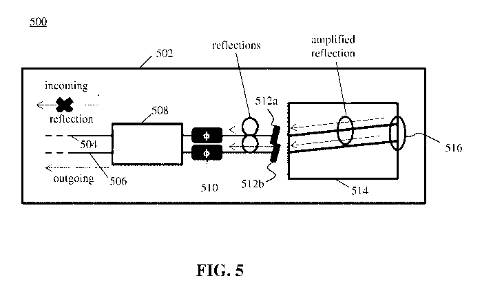
[0040] FIG. 5 illustrates a photonic integrated circuit 500 according to an
embodiment. Photonic
integrated circuit 500 includes many similar elements to the previously
described photonic
integrated circuits 200 and 300. Elements such as substrate 502, first and
second waveguides
504 and 506, coupling region 508, optical modulators 510, and facets 512a and
512b will not be
described again in detail, except as they apply to this embodiment using an
optical amplifier 514.
An example of optical amplifier 514 is a semiconductor optical amplifier
(BOA).
[0041] Optical amplifier 514 may be a single element aligned to both facets
512a and 512b, or it may
include two separate amplifying units coupled to each facet, respectively.
Optical amplifier 514
may include a reflective coating 516 to increase the amount of reflected light
within an active gain
region of optical amplifier 514. Eventually, amplified light will couple back
into first waveguide
504 and second waveguide 506. As illustrated in FIG. 5, reflections will also
occur from facets
512a and 512b.
[0042] Ideally, the amplified light propagating back towards coupling region
508 in each of first
waveguide 504 and second waveguide 506 is the same. This would theoretically
occur if coupler
CA 02979306 2017-09-11
WO 2016/142464
PCT/EP2016/055117
7
region 508 was perfectly balanced, the amplification occurring for both beams
being fed back into
first waveguide 504 and second waveguide 506 is identical and equally biased,
and the quality of
optical coupling is equal at both interfaces. However, in practice, this
situation is nearly
impossible to produce. One or more optical modulating elements 510 may be
implemented to
shift the phase of the reflected, amplified light. According to an embodiment,
the phase of the
reflected light in both waveguides 504 and 506 is shifted such that the
reflected light in both
waveguides constructively interfere within second waveguide 506 and
destructively interfere
within first waveguide 504 after passing through coupling region 508. In this
way, the amplified
light does not interfere with the input light in first waveguide 504.
[0043] Optical amplifier 514 may be integrated within substrate 502. In this
way, the same etching steps
may be performed when fabricating the device to define both waveguides 504 and
506 as well as
the gain region of optical amplifier 514. This monolithic integration allows
for very good alignment
between facets 512a and 512b and optical amplifier 514. In another example,
optical amplifier
514 may be fabricated on a separate substrate and bonded to substrate 502.
This may allow for
the creation of a very high gain region when using particular materials better
suited for optical
amplifier 514, but may make alignment with facets 512a and 512b more
difficult. Reflected light
may be amplified within optical amplifier 514 using methods well known to one
skilled in the art,
such as optical or electrical pumping.
[0044] FIG. 6 illustrates a photonic integrated circuit 600 according to an
embodiment. Photonic
integrated circuit 600 shares many similarities with photonic integrated
circuit 300 except for the
inclusion of optical amplifier 618. Like photonic integrated circuit 300,
photonic integrated circuit
600 has substrate 602, first waveguide 604, second waveguide 606, first
coupling region 608,
second coupling region 610, first set of optical modulating elements 614 and
second set of optical
modulating elements 612. End facets 616a and 616b are aligned with optical
amplifier 618.
[0045] In an embodiment, first coupling region 608 and second coupling region
610 are arranged as a
Mach-Zehnder interferometer. This may allow for power to be accurately
balanced between both
first waveguide 604 and second waveguide 606 using second set of optical
modulating elements
612, while phase may be independently controlled in the waveguide segments
using first set of
one or more optical modulating elements 614. Alternatively, this arrangement
has an advantage
of being capable of directing reflections from facets 616a and 616b separately
from reflected light
that was amplified in optical amplifier 618. For example, the reflections from
facets 616a and
616b may have their phase adjusted to only be output at waveguide 604 after
passing through
both first coupling region 608 and second coupling region 610 while the
amplified reflections may
have their phase adjusted to only be output at waveguide 606 after passing
through both first
coupling region 608 and second coupling region 610. This approach may also be
used to
compensate for inaccuracies in fabrication, imperfect cleaning or coupler
imbalance. Higher
order implementations may also be considered for further compensation of
imbalance over a
given wavelength range, or in different polarization states.
[0046] An example interferometer arrangement that may be used to perform OCT
on a sample is
illustrated in FIG. 7. Various embodiments of an optical integrated circuit as
illustrated in FIGs. 2-
CA 02979306 2017-09-11
WO 2016/142464
PCT/EP2016/055117
8
3 and 5-6 may be included within OCT system 701 to help mitigate the effects
of undesirable
reflections that would degrade the signal received at the detector. OCT system
701 includes an
optical source 702, a splitting element 704, a sample arm 706, a reference arm
708, a delay unit
712, and a detector 714. Delay unit 712 may include various light modulating
elements. These
modulating elements may perform phase and/or frequency modulation to
counteract undesired
optical effects in the light, and to select one or more depths of sample 710
to be imaged. The
use of the term "light" may refer to any range of the electromagnetic
spectrum. In an
embodiment, the term "light" refers to infrared radiation at a wavelength of
about 1.3 pm.
[0047] In the embodiment shown, delay unit 712 is located within reference arm
708. However, it should
be understood that delay unit 712 may instead be located in sample arm 706.
Alternatively,
various elements of delay unit 712 may be present in both sample arm 706 and
reference arm
708. For example, elements of delay unit 712 that introduce a variable delay
to the light may be
located in sample arm 706, while elements that modulate different polarization
modes of the light
may be located in reference arm 708. In one example, sample arm 706 and
reference arm 708
are optical waveguides, such as patterned waveguides or optical fibers. In an
embodiment, all of
the components of OCT system 701 are integrated onto a planar lightwave
circuit (PLC). In
another embodiment, at least the components within delay unit 712 are
integrated on the same
substrate of an optical integrated circuit. Other implementations may be
considered as well, such
as, for example, fiber optic systems, free-space optical systems, photonic
crystal systems, etc.
[0048] It should be understood that OCT system 701 may include any number of
other optical elements
not shown for the sake of clarity. For example, OCT system 701 may include
mirrors, lenses,
gratings, splitters, micromechanical elements, etc., along the paths of sample
arm 706 or
reference arm 708.
[0049] Splitting element 704 is used to direct light received from optical
source 702 to both sample arm
706 and reference arm 708. Splitting element 704 may be, for example, a bi-
directional coupler,
an optical splitter, or any other modulating optical device that converts a
single beam of light into
two or more beams of light. Splitting element 704 may incorporate, for
example, one or more
photonic circuits described with respect to FIGS. 2A, 3A, 5, and 6.
[0050] Light that travels down sample arm 706 ultimately impinges upon sample
710. In an
embodiment, sample arm 706 includes a waveguide that guides the light towards
one or more of
addressable elements 902. Sample 710 may be any suitable sample to be imaged,
such as
tissue. The light scatters and reflects back from various depths within sample
710, and the
scattered/reflected radiation is collected back into sample arm 706. In
another embodiment, the
scattered/reflected radiation is collected back into a different waveguide
than the transmitting
waveguide. The scan depth may be chosen via the delay imposed on the light
within delay unit
712.
[0051] Light within sample arm 706 and reference arm 708 is recombined before
being received at
detector 714. In the embodiment shown, the light is recombined by splitting
element 704. In
another embodiment, the light is recombined at a different optical coupling
element than splitting
element 704. Detector 714 may include any number of photodiodes, charge-
coupling devices,
CA 02979306 2017-09-11
WO 2016/142464
PCT/EP2016/055117
9
and/or CMOS structures to transduce the received light into an electrical
signal. The electrical
signal contains depth-resolved optical data related to sample 710 and may be
received by a
processing device for further analysis and signal processing procedures. As
used herein, the
term "depth-resolved" defines data in which one or more portions of the data
related to specific
depths of an imaged sample can be identified.
[0052] Optical source 702 may include one or more light emitting diodes (LEDs)
or laser diodes. For
example, LEDs may be used when performing time domain and/or spectral domain
analysis,
while tunable lasers may be used to sweep the wavelength of the light across a
range of
wavelengths.
[0053] OCT system 701 is illustrated as an interferometer design similar to a
Michelson interferometer,
according to an embodiment. However, other interferometer designs are possible
as well,
including Mach-Zehnder or Mireau interferometer designs.
[0054] It is to be appreciated that the Detailed Description section, and not
the Summary and Abstract
sections, is intended to be used to interpret the claims. The Summary and
Abstract sections may
set forth one or more but not all exemplary embodiments of the present
invention as
contemplated by the inventor(s), and thus, are not intended to limit the
present invention and the
appended claims in any way.
[0055] Embodiments of the present invention have been described above with the
aid of functional
building blocks illustrating the implementation of specified functions and
relationships thereof.
The boundaries of these functional building blocks have been arbitrarily
defined herein for the
convenience of the description. Alternate boundaries can be defined so long as
the specified
functions and relationships thereof are appropriately performed.
[0056] The foregoing description of the specific embodiments will so fully
reveal the general nature of
the invention that others can, by applying knowledge within the skill of the
art, readily modify
and/or adapt for various applications such specific embodiments, without undue
experimentation,
without departing from the general concept of the present invention.
Therefore, such adaptations
and modifications are intended to be within the meaning and range of
equivalents of the
disclosed embodiments, based on the teaching and guidance presented herein. It
is to be
understood that the phraseology or terminology herein is for the purpose of
description and not of
limitation, such that the terminology or phraseology of the present
specification is to be
interpreted by the skilled artisan in light of the teachings and guidance.
[0057] The breadth and scope of the present invention should not be limited by
any of the above-
described exemplary embodiments, but should be defined only in accordance with
the following
claims and their equivalents.