Note : Les descriptions sont présentées dans la langue officielle dans laquelle elles ont été soumises.
CA 02983389 2017-10-19
WO 2016/175688
PCT/SE2015/050476
1
DRIFT COMPENSATION
Technical field
The invention disclosed herein generally relates to serial production of
electric circuits and technology for operating such circuits. In particular,
it re-
lates to methods and devices for manufacturing and operating realizations of
a predefined electric circuit design in a manner to reduce the impact of envi-
ronment-induced drift. It further relates to a signal processing device
compris-
ing a realization of a predefined electric circuit and a compensation stage
configured to compensate drift in relation to a reference behaviour of the
elec-
tric circuit design generally or to a reference behaviour of the specific
realiza-
tion of the electric circuit design.
Background
In an electric circuit experiencing drift, a change in an environment
condition leads to a normally undesirable change in an operational property of
the circuit. Operational properties may include voltage, current, frequency,
phase, amplitude, total power, power spectrum, delay, polarization and modu-
lation characteristics. Environment conditions may include external factors,
such as fluctuations in ambient temperature, internal temperature, humidity or
magnetic flux density, but also internal factors such as variations in signals
that are generated expressly for use by the electric circuit, e.g., signals in
electric or optical form supplying the circuit with energy, input data or
other
information. An environment condition may be quantitatively described by a
value of an environment parameter.
In a general approach illustrated in figure 1A, a circuit 110õ,, 120õ, is
modelled as a device producing an output signal y(t) in response to an input
signal x(t) that the circuit currently receives. If the circuit is assumed to
be
approximately time-invariant and the input and output signals are modelled as
(combinations of) periodic functions of time, the circuit can be characterized
quantitatively in terms of its gain G(w) or phase 4)(w) at different values of
the
frequency w. The term frequency response is used to refer to a collection of
CA 02983389 2017-10-19
WO 2016/175688
PCT/SE2015/050476
2
gain or phase values, or both, for frequencies in a relevant frequency range
wa 5 w 5 wb. In the present disclosure, the general notation Q(w) is meant to
cover both gain, phase and any combined representation of both these quan-
tities (complex or otherwise two-dimensional, such as
Q(w) = G(w)exp(/il)(co)) ). The operational properties of a circuit that
change
because of drift may include gain or phase, or both.
The precise drift behaviour of a circuit may differ quantitatively or quali-
tatively between different operating frequencies. The frequency dependence
of an electric property's drift may be captured by measuring a series of fre-
quency responses under different environment conditions, e.g. a collection of
stable values of an observable environment parameter. An equivalent alterna-
tive may be to measure the electric property at a collection of stable
operating
frequencies while the environment conditions are changing in a known fash-
ion.
Other than artificial stabilization of a circuit's operating environment, it
has been a commonly practised approach for reducing the negative of drift to
make direct measurements and then apply a corresponding compensation.
The compensation may for instance aim to approach the current output signal
(or frequency response) of the circuit to a reference signal (or reference fre-
quency response). The effective drift, i.e. with compensation applied, is
thereby reduced.
The applicant's earlier disclosure W01 4094823A1 is cited as one ex-
ample, where techniques for compensating a frequency-dependent in-
phase/quadrature channel mismatch are proposed. Direct measurements
may be an attractive option for circuits operating under changing environment
conditions, since drift-induced variations are captured as part of the
measured
signal, and may ultimately be compensated. The approach based on direct
measurements may however be computationally costly or otherwise respond
relatively slowly.
From the applicant's application W01 0069365A1, it is furthermore
known that a nonlinearity error in an analog-to-digital converter (ADC) can be
estimated ¨ and ultimately compensated ¨ using a plurality of linear filters
in
accordance with a discrete-time model of the converter that mimics the ADC's
3
behaviour. According to that disclosure, the discrete-time model is tuned to
each individual ADC by applying test signals and measuring the correspond-
ing output signal energy. This approach is advantageous by its relatively mod-
est computational expense and low algorithmic delay, but could have accu-
racy problems unless the ADC is operated under stable environment condi-
tions.
Summary
It is an object of the present invention to propose methods and devices
for manufacturing realizations of an electric circuit design that may be oper-
ated while experiencing a reduced effective drift, e.g., by proposing a tech-
nique for correcting the respective output signals of the realizations by a
com-
pensation signal. It is a further object to propose such manufacturing methods
and devices with an improved throughput per unit time. It is a still further
ob-
ject to propose methods and devices for operating a realization of the
electric
circuit design with a reduced effective drift despite changing environment con-
ditions.
Considered are electric circuits, in particular semiconductor circuits or
integrated circuits, that have been manufactured in accordance with a prede-
fined electric circuit design. Example types of circuit designs include:
analog-
to-digital converter, digital-to-analog converter, upconversion mixer, downcon-
version mixer, frequency modulator, frequency demodulator, programmable-
gain amplifier, low-noise amplifier as well as amplifiers in general. At least
one input¨output signal pair may be identified for the electric circuit
design,
wherein the input signal and output signal may be electric signals themselves,
or may alternatively be received or generated optically, mechanically, acousti-
cally or by a different physical form of energy, using suitable transducers.
The
electric circuits may be seen as (physical) realizations of the electric
circuit
design; furthermore, they may be said to belong to a main lot of realiza-
Date Recue/Date Received 2021-10-12
CA 02983389 2017-10-19
WO 2016/175688
PCT/SE2015/050476
4
tions. The electric circuits may have been serially produced (or produced in a
relatively large quantity, or produced on an industrial scale, or mass pro-
duced). A design-specific model has been defined in order to describe a fre-
quency response of all realizations of the electric circuit design in depend-
once of at least one environment parameter (see previous section for exam-
ples). In particular, the design-specific model may predict distinct frequency
responses, and typically does so, for distinct values of the environment pa-
rameter. While the accuracy of the design-specific model may be satisfactory
in relation to some or most realizations, manufacturing defects, material de-
fects and other irregularities may cause the accuracy to be reduced in
relation
to other realizations.
In one embodiment, a unit in the main lot of realizations undergoes all
of the following. First, a unit-specific frequency response is recorded (or
measured) at a stable value of the environment parameter(s), by performing
measurements on the unit. The design-specific model, when evaluated at the
stable value of the environment parameter(s), is then fitted to the unit-
specific
frequency response, whereby a unit-specific model is obtained, which de-
scribes a frequency response for the unit in dependence of the environment
parameter(s). Finally, data representing the unit-specific model thus obtained
.. is stored in association with the unit. This embodiment may achieve the
object
of manufacturing the electric circuit design so that at least one of its
realiza-
tions may be operated at reduced effective drift, since the stored data may be
accessed and used to predict the drift behaviour of the realization (in terms
of
changes in its frequency response) in a context where the realization is oper-
ated.
The data representing the unit-specific model may be stored in the re-
alization in a local memory, which is accessible from a connected device. Al-
ternatively, the data is stored in a memory of a compensation stage config-
ured to be operated in association with the realization, or in a memory that
.. such compensation stage may access during operation. Further alternatively,
the data may be stored in a networked library, at a location marked with an
identifier of the realization with which it is associated.
CA 02983389 2017-10-19
WO 2016/175688 PCT/SE2015/050476
The unit-specific model may be represented and stored as a finite table
of values. During operation of the unit, this table is read out by a compensa-
tion stage, which may optionally interpolate between the read values. Alterna-
tively, the unit-specific model may be represented by a formula (analytic ex-
5 pression depending on frequency and the environment parameter(s)), the
numeric parameters of which have been fitted to the unit after the unit has
been manufactured, and which is evaluated during operation to enable com-
pensation. The representation of the model as a formula may sometimes be
more storage-efficient.
In one embodiment, the compensation stage with which the realization
operates is configured to determine a present value of the environment pa-
rameter(s) and to compensate drift based thereon in relation to a reference
frequency response, which is independent of the environment parameter(s).
In particular, the compensation may include evaluating the unit-specific model
at the determined present value of the environment parameter(s) and to de-
termine the amount of compensation needed to reach agreement with the
reference frequency response within a desired accuracy. More precisely, the
compensation may include determining a current operating frequency and
evaluating the frequency response (i.e., gain, phase or both) at the current
operating frequency and at the determined value of the environment parame-
ter(s). It is preferred that compensation is effected in the digital domain.
As
such, in the types of circuit designs mentioned above, it is preferred that
the
compensation stage is arranged on a side of the circuit where signals are rep-
resented in digital form.
In one embodiment, the design-specific model is prepared based on
information from measurements that have been performed on realizations
belonging to a test lot of realizations of the electric circuit design. As
used in
this disclosure, a realization belongs to the "main lot" unless it belongs to
the
"test lot". The main lot may be produced on one or more parallel production
lines having substantially equivalent production equipment and using sub-
stantially equivalent raw materials, While relatively extensive measurements
may be performed on the realizations in the test lot (e.g., recording of fre-
quency responses for plural values of the environment parameter(s) or
CA 02983389 2017-10-19
WO 2016/175688
PCT/SE2015/050476
6
equivalently, recording a response at a collection of fixed frequencies for
changing values of the environment parameter(s)), the main lot is produced
under normal cost pressure, whereby the measuring may be reduced towards
the minimal amount that is thought sufficient to guarantee that the perform-
ance of each realization lies within commercially acceptable bounds, Also for
profitability reasons, it is normally to be avoided to make the test lot more
numerous than justified, whereas the main lot is not restricted as to its
total
number, rather the main lot should comprise a large number of realizations to
benefit from economies of scale. The test lot may be produced as a separate
test series using the same production equipment as will be used for the main
lot. Alternatively, the test lot is formed by extracting produced samples from
the main lot while serial production is running; this means that the main lot
need not be produced at a later point in time than the test lot. In this
alterna-
tive approach, no complete design-specific model will be available when the
earliest units are being produced; instead, one may revert to the earliest
units
later, record frequency responses at stable values of the environment pa-
rameter(s) and define unit-specific models for those units as described above.
On M1 realizations in the test lot, a number N of frequency responses
are recorded, each for a stable value of the environment parameter(s). One or
more frequency responses are recorded for each realization. It is not neces-
sary for all frequency responses to be recorded at identical (sets of) values
of
the environment parameter(s). While not essential to the present embodi-
ment, a certain variation in the environment parameter(s) is in fact
desirable,
so that the design-specific model may be defined on the basis of data points
that are distributed over the contemplated working range of the electric
circuit
design. Likewise, it is advantageous to perform measurements on more than
one single realization of the electric circuit design, and preferably produced
by
different production lines if plural lines are provided, so that individual
irregu-
larities are 'averaged out' and neutralized. Hence, the number M1 of realize-
tions in the test lot, just like the number N of frequency responses recorded
for these, are to be chosen in view of the following factors:
i) Higher cost pressure from market = decrease M1 or N or both.
CA 02983389 2017-10-19
WO 2016/175688
PCT/SE2015/050476
7
ii) Wider required working range (environment parameter(s)) = in-
crease N.
iii) Higher variation between realizations = increase M1.
In an approach where the design-specific model is refined progressively by
fitting it to more and more data points, a high variation between realizations
(third factor) may translate into slow convergence of the model. It is noted
that
in such circumstances, the accuracy of the design-specific model is not nec-
essarily a factor that limit the performance for a specific realization of the
de-
sign; instead, an increased effort into fitting the design-specific model to
indi-
vidual realizations may be a more efficient measure to take.
In one embodiment, temperature may be an environment parameter,
on which the design-specific model depends. To cover the working range effi-
ciently, some frequency responses for the test lot may be recorded at ambient
temperature (e.g., laboratory temperature), others while artificial cooling or
heating is applied. This cooling or heating may be stabilized using feedback
control, so that the frequency response is recorded at a reasonably stable
temperature. A similar technique may be adopted for stabilizing other envi-
ronment parameters in order for the measurements on the test lot to be of
high reliability.
In one embodiment, the step of fitting the design-specific model
to the frequency response recorded for a specific unit (in the main lot) may
include determining a unit-specific calibration term that approximates a devia-
tion between the design-specific model, when evaluated for said stable value
of the environment parameter(s), and the unit-specific frequency response on
the other. The unit-specific calibration term may be frequency-independent, or
may vary with frequency. In the latter case, the unit-specific calibration
term
may correspond to a function of frequency being a difference between, on the
one hand, the frequency response that the design-specific model predicts for
the value of the environment parameter(s) and, on the other hand, the actual
frequency response recorded for the specific unit in the main lot.
Alternatively,
if a proportional gain less than unity is applied, the unit-specific
calibration
term may correspond to a downscaled version of this difference.
CA 02983389 2017-10-19
WO 2016/175688
PCT/SE2015/050476
8
In one embodiment, the design-specific model may comprise two mu-
tually independent contributions: one basic frequency response (function of
frequency only) and one compensation term (function of the environment pa-
rameter(s) and optionally of frequency). Since these contributions are based
on collective quantities computed from measurements for the test lot, both are
unit-independent. A unit-specific model, applicable for a unit in the main
lot,
may therefore comprise three mutually independent contributions, namely the
unit-independent basic frequency response, the unit-independent cornpensa-
tion term and the unit-specific calibration term (function of frequency only).
In
mathematical formalism, letting w denote frequency, letting T and V be ex-
ample environment parameters, and letting m be an index identifying the unit
for which the unit-specific model is derived, the contributions on their most
general form may be written: Q0(w), P(w; T, V), Rm(w). The unit-specific
model may therefore be separated into three terms that are susceptible to
independent evaluation: Qm(w; T, V) = Q0(w) + P(w; T, V) + Rni(w). It is re-
called that the unit-independent compensation term P and the unit-specific
calibration term R, may be constant with respect to frequency. It is noted
that
a unit-specific model may be represented by two types of stored data, namely
data having been prepared on the basis of a plurality of frequency responses
measured for a test lot of realizations of the electric circuit design (first
type)
and data having been prepared on the basis of a measurement of a unit-
specific frequency response for the unit, at a stable value of the environment
parameter(s). Importantly, the data of the second type may have been pre-
pared on the basis of a measurement of a single frequency response, or at
least on the basis of a small number of measurements that would alone have
been insufficient for defining a statistically reliable model of the unit's
fre-
quency response.
In one embodiment, an environment parameter, on which the design-
specific model depends, may be the value of a supply voltage (or drive volt-
age) for powering the electric circuit design.
In one embodiment, an environment parameter, on which the design-
specific model depends, may be the value of a gain of a pre-amplifier, with
which the electric circuit design is configured to cooperate. Pre-
amplification
CA 02983389 2017-10-19
WO 2016/175688
PCT/SE2015/050476
9
may be practised in connection with ADCs (or digitizers) in an I/Q modulator
or I/Q demodulator.
As already noted, the reference frequency response can be assigned
independently for each realization of the electric circuit design. The
reference
frequency response is normally a function independent of the environment
parameter(s). The reference frequency response for a particular realization of
the electric circuit design may be selected in accordance with a currently de-
sired goal, such as reduction of particular realization's drift, or reduction
of
two realizations' relative drift, or reduction of mutual drift between the
units in
a group of realizations, or equalizing frequency responses of two or more re-
alizations throughout the environment parameter(s) range. Some of these
goals may only be achieved if the reference frequency response is independ-
ently assignable for each realization.
In one embodiment, a first realization of the electric circuit design is
operated in conjunction with a second realization and with a compensation
stage configured to compensate drift of at least the first realization. In
this
embodiment, the reference frequency response is a frequency response of
the second realization. In this connection, the second realization is used as
a
reference regardless of any drift it experiences with respect to the environ-
ment parameter(s). Alternatively, the second realization is compensated (by
the same or by a further compensation stage) to have reduced drift, and the
reference frequency response for the first realization is chosen in such man-
ner that it mimics the behaviour of the compensated second realization. In
this connection, the reference frequency response for the second realization
may be chosen to simplify the drift compensation task as far as possible, in
particular, by choosing a reference frequency response that is close (in a
suitable sense, such as L1 or L2 norm) to the actual frequency response in the
greater part of the working range. This arrangement may help reduce errors
deriving from a pairwise mismatch between two circuits, such as I/Q imbal-
ance errors and errors associated with time-interleaved ADC
Time-interleaved ADCs is one example application where two or more
realizations of the same electric circuit design are arranged in parallel and
where uncontrolled deviations between the realizations could degrade the
CA 02983389 2017-10-19
WO 2016/175688
PCT/SE2015/050476
accuracy of the ADC. Temperature and supply voltage are preferred as envi-
ronment parameters in this connection.
I/Q modulators and I/Q demodulators is a further example application
where two realizations of a same electric circuit design are operated in con-
5 junction, more precisely two ADCs in parallel branches of the modulator
or
demodulator. In this connection, the compensation stage may be an I/O mis-
match (channel mismatch) compensator that may be configured to correct
one of the respective ADC output signals (corresponding to each of the I and
Q channels). Alternatively, correction is applied downstream of a data de-
10 modulator that processes the I and Q channels and combines these into a
common output signal. If a preamplifier is arranged upstream of the ADCs (in
particular a variable-gain amplifier, such as one preamplifier upstream of the
respective ADC in each branch of the I/Q modulator or I/Q demodulator, or a
common preamplifier upstream of both branches), the characteristics of the
signal vary with the present gain of the preamplifier(s). The inventors have
realized that the preamplification gain and/or other settings influencing the
behaviour of the preamplifier(s) (collectively: gain state) is relevant as an
en-
vironment parameter in the above sense. This is to say, the design-specific
model may predict different frequency responses for different gain states in
.. this embodiment.
In one embodiment, the electric circuit design relates to an ADC for
converting an analog input signal into a digital output signal. The reference
frequency response may for such a design be unit-independent in the sense
that a plurality of realizations are compensated according to identical copies
of a reference frequency response. This may achieve the double purpose of
reducing drift and reducing imperfections, such as nonlinearities of the
electric
circuit design. The inventors have realized that an advantageous combination
of environment parameters is supply voltage and temperature.
In one embodiment, the data representing the unit-specific model may
express a difference between an actual frequency response and a reference
frequency response. Alternatively, the data may express a ratio of the actual
frequency response and the reference frequency response. The frequency
response may include gain, phase, or a combination of these quantities. This
CA 02983389 2017-10-19
WO 2016/175688
PCT/SE2015/050476
11
is an advantageous way of representing the unit-specific model, since on av-
erage, the values to be represented will normally be close to zero (for a dif-
ference) or close to one (for a ratio). Such values can be efficiently
quantized
using an entropy-coding approach.
In a further aspect, a manufacturing system comprising a number of
sections that cooperate to realize a predefined electric circuit of the type
de-
scribed above. The sections of the system may be co-located, in particular
physically connected or otherwise integrated, or may alternatively be distrib-
uted geographically. In one embodiment, the manufacturing system corn-
prises a memory storing a design-specific model of the electric circuit
design,
an assembly section for producing yet uncalibrated realizations of the
electric
circuit design, and a calibration section which is communicatively coupled to
the memory. In normal operation, all realizations produced by the assembly
section will be calibrated by the calibration section, The calibration section
specifically comprises: an analyzer for measuring a frequency response of a
produced unit, an environment sensor for determining the environment condi-
tions under which such frequency response is measured (practically, by
measuring a value of the environment parameter(s) referred to above), and a
device programmer for fitting the design specific model to the measured fre-
quency response, and thereby obtaining a unit-specific model, of which a rep-
resentation is to be stored in association with the unit. The frequency re-
sponse is preferably measured at an approximately stable value of the envi-
ronment parameter(s).
Because only a limited amount of measurements are needed for the
realizations in the main lot, the proposed manufacturing system may be im-
plemented to have a high throughput per unit time, thereby fulfilling one of
the
above objects of the invention.
In one embodiment, the manufacturing system further comprises a
testing section, in which a testing environment sensor, a testing analyzer and
a processor cooperate to define the design-specific model on the basis of
measurements on a test lot of realizations of the electric circuit design. As
already described, while one of said realizations is maintained at a stable
value of the environment parameter(s), a frequency response is measured for
CA 02983389 2017-10-19
WO 2016/175688
PCT/SE2015/050476
12
the realization. Data (frequency responses) is collected for all realizations
in
the test lot and preferably for different stable (sets of) values of the
environ-
ment parameter(s), whereby the design-specific model can be defined. Data
representing the design-specific model is stored in the memory of the manu-
facturing system, where it may be accessed by the calibration section.
In a further aspect, a signal processing device comprises a unit which
is a realization of a predefined electric circuit design, a memory storing
data
representing a unit-specific model descriptive of the unit, and a compensation
stage configured to compensate drift in relation to a reference frequency re-
sponse, on the basis of the unit-specific model and a value of one or more
environment parameters, on which the unit-specific model depends, The
compensation stage may determine the value of the environment parame-
ter(s) using an environment sensor, such as a local thermometer. Alterna-
tively, the compensation stage obtains this information from another corripo-
nent of the signal processing device, such as a voltmeter arranged to deter-
mine a present value of a supply voltage.
In one embodiment, the memory of the signal processing device stores
data of a least two types representing quantitative aspects of the unit-
specific
model. As explained above, data of the first type has been derived based on
a relatively larger number of measurements (on the test lot), while data of
the
second type has been derived based on one or a relatively smaller number of
measurements (on the unit, as part of the main lot).
In a further aspect, a unit which is a realization of a predefined electric
circuit design is operated with drift compensation by referring to data repre-
senting a unit-specific model of the kind described above. More precisely, a
present value of an environment parameter on which the model depends is
determined, the model is evaluated for the present value, and appropriate
correction is applied in order to compensate the unit's deviation from a refer-
ence frequency response. In particular, the compensation may include deter-
mining a current operating frequency, evaluating the model and the reference
frequency response for this frequency only, and applying local compensation.
When local compensation is applied, it may be sufficient to obtain only such
13
data that represents the unit-specific model at or near the current operating
frequency.
In different implementations, the data representing the unit-specific
model may be stored in the unit or an associated memory, or may be re-
trieved from a networked library in a location designated by a unique
identifier
associated with the unit.
As noted above, the data representing the unit-specific model may re-
late to a look-up table, or an expression that can be evaluated for concrete
values of variables of which the expression depends. The expression may
contain elementary algebraic or transcendental functions or simple special
functions, or a combination of these. In particular, the expression may be a
polynomial of order less than ten, preferably less than five, such as less
than
four, such as a cubic or quadratic polynomial.
In a further aspect, there is provided a computer program product corn-
prising a computer-readable medium with instructions for causing a program-
mable computer to execute one of the methods described above. Examples
of computer-readable media are given below.
In one embodiment, there is provided a method associated with a pre-
defined electric circuit design, wherein each electric circuit manufactured in
accordance with the electric circuit design defines a frequency response be-
tween an input signal and an output signal in a frequency range, the method
comprising: i) defining, based on measurements on a test lot of electric
circuits manufactured in accordance with the electric circuit design, a design-
specific model for the electric circuit design, the design-specific model
describing a
frequency response of the electric circuit design in dependence of at least
one parameter affecting operation of the electric circuit design; and for a
unit
in a main lot of electric circuits manufactured in accordance with the
electric
circuit design, wherein the main lot includes electric circuits outside the
test lot
of electric circuits, and wherein the unit is outside the test lot of electric
cir-
cults: ii-1) obtaining a unit-specific frequency response as a frequency re-
sponse for the unit measured at a certain value of the at least one parameter;
ii-2) fitting the design-specific model at the certain value of the at least
one
parameter to the unit-specific frequency response, whereby a unit-
Date Recite/Date Received 2023-06-13
13a
specific model for the unit is obtained describing a frequency response for
the
unit in dependence of the at least one parameter; and ii-3) storing, in
associa-
tion with the unit, data representing the unit-specific model.
In one embodiment, there is provided a manufacturing system for man-
ufacturing electric circuits in accordance with a predefined electric circuit
de-
sign, wherein each electric circuit defines a frequency response between an
input signal and an output signal in a frequency range, the manufacturing sys-
tem comprising: a testing section configured to define, based on measure-
ments on a test lot of electric circuits manufactured in accordance with the
electric circuit design, a design-specific model for the electric circuit
design,
the design-specific model describing a frequency response of the electric cir-
cuit design in dependence of at least one parameter affecting operation of the
electric circuit design; a memory for storing the design-specific model; an as-
sembly section for producing electric circuits manufactured in accordance
with the electric circuit design that are due for calibration; and a
calibration
section comprising: a sensor for measuring the at least one parameter; an an-
alyzer arranged in proximity of the sensor and being configured to obtain, for
a
unit being an electric circuit outside the test lot of electric circuits and
pro-
duced by the assembly section, a unit-specific frequency response as a fre-
quency response for the unit measured at a certain measured value of the at
least one parameter; and a device programmer configured to fit the design-
specific model to the unit-specific frequency response at the certain value of
the at least one parameter, whereby a unit-specific model for the unit is ob-
tained describing a frequency response for the unit in dependence of the at
least one parameter, and to store, in association with the unit, data
represent-
ing the unit-specific model.
In one embodiment, there is provided a signal processing device com-
prising: a unit being an electric circuit manufactured in accordance with a
pre-
defined electric circuit design; a memory storing data representing a unit-spe-
cific model for the unit, the unit specific model describing a frequency re-
sponse between an input signal and an output signal of the unit, in a fre-
quency range, in dependence of the at least one parameter T affecting opera-
tion of the electric circuit design; and a compensation stage configured to
Date Recite/Date Received 2023-06-13
13b
retrieve the data from the memory, to determine a present value of the at
least one parameter, and, based on the present value and the unit-specific
model, to compensate a deviation between a frequency response of the unit
and a reference frequency response, wherein the reference frequency re-
sponse is independent of the at least one parameter, wherein the memory
stores at least data of a first type and data of a second type representing
the
unit-specific model, the first type having been prepared on the basis of a plu-
rality of frequency responses measured for a test lot of electric circuits
manu-
factured in accordance with the electric circuit design, and the second type
having been prepared on the basis of a measurement of a unit-specific fre-
quency response for the unit at a certain value of the at least one parameter
wherein the unit is outside the test lot of electric circuits manufactured in
ac-
cordance with the electric circuit design.
In one embodiment, there is provided a method of operating a unit be-
ing an electric circuit manufactured in accordance with a predefined electric
circuit design, the method comprising: obtaining data representing a unit-spe-
cific model for the unit, the unit-specific model describing a frequency re-
sponse between an input signal and an output signal of the unit, in a fre-
quency range, in dependence of at least one parameter affecting operation of
the electric circuit design; determining a present value of the at least one
pa-
rameter, and based on the present value and the unit-specific model, com-
pensating a deviation between a frequency response of the unit and a refer-
ence frequency response, wherein the reference frequency response is inde-
pendent of the at least one parameter, wherein the data includes data of a
first type and data of a second type, the first type having been prepared on
the basis of a plurality of frequency responses measured for a test lot of
elec-
tric circuits manufactured in accordance with the electric circuit design, and
the second type having been prepared on the basis of a measurement of a
unit-specific frequency response for the unit at a certain value of the at
least
one parameter wherein the unit is outside the test lot of electric circuits
manu-
factured in accordance with the electric circuit design.
It is noted that features from the embodiments described above may
be combined to form new embodiments without departing from the scope of
Date Recue/Date Received 2022-08-05
13c
the invention. This holds true also in cases where the features have been re-
cited in mutually different claims, unless the features are technically incom-
patible.
Brief description of the drawings
Embodiments will now be described in greater detail and with refer-
ence to the accompanying drawings, on which:
figure 1A shows an electric circuit design;
figure 1B shows an electric circuit design and a corresponding corn-
pensation stage, according to one embodiment;
figure 2 shows a manufacturing system for realizing an electric circuit
design, according to one embodiment;
figure 3 shows an electric circuit design with an integrated memory for
storing a unit-specific model, according to one embodiment;
Date Recue/Date Received 2021-10-12
CA 02983389 2017-10-19
WO 2016/175688 PCT/SE2015/050476
14
figure 4 shows a signal processing device with an integrated cornpen-
sation stage and memory for storing a unit-specific model, according to one
embodiment;
figure 5 shows a detail of a I/Q demodulator with a compensation stage
according to one embodiment;
figure 6 shows a time-interleaved ADC with N 2 parallel subconvert-
ers and a compensation stage according to one embodiment;
figures 7A, 7B, 7C and 7D show details of time-interleaved ADCs each
having four parallel subconverters and at least one compensation stage ac-
cording to one embodiment; and
figure 8 shows a detail of a frequency demodulator with a compensa-
tion stage according to one embodiment.
All figures are schematic and generally show only parts that are neces-
sary for the purpose of elucidating the invention, whereas other parts may be
omitted or merely suggested.
Detailed description of embodiments
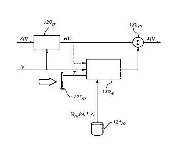
Figure 1A has been briefly discussed above. Figure 1B shows an iden-
tical unit 120m, which is a realization (in the main lot) of a predefined
electric
circuit design that is operated in conjunction with a compensation stage 130m.
The compensation stage 130m may serve the unit 120m or additional units as
well. For the purposes of compensating drift in the unit 120m, however, the
compensation stage 130m retrieves data representing a unit-specific model
Qm(w; T, V) from a memory 121m. The unit-specific model predicts a fre-
quency response (including gain, phase or a combination of these quantities)
for each value in the allowed range of the operating frequency w and two en-
vironment parameters T and V. The allowed range may for instance be a
neighbourhood of a triple of nominal values (wo, To, Vo). In the example, the
unit-specific model takes into account the effect of one internal and one ex-
temal quantity, wherein the internal quantity is being read out directly from
an
electric line, and the external quantity is measured using a sensor 131m. In
variations to this embodiment, the unit-specific model may consider only ex-
ternal or only internal factors, or a combination of any number of each. In
the
CA 02983389 2017-10-19
WO 2016/175688
PCT/SE2015/050476
example, the unit-specific model depends of a supply voltage of V [volt], with
which the unit 120m is driven, and a temperature of T [Kelvin]. Here, the volt-
age can be read out directly from a line parallel to the supply voltage line
into
the unit 120m, whereas a dedicated temperature sensor 131m is arranged in
5 proximity of the unit 120m and communicatively connected to the compensa-
tion stage 130m.
The compensation stage 130m may optionally receive the output signal
y(t) of the unit 120m, based on which it may determine a current operating
frequency w. It is emphasized that the compensation stage 130m need not
10 use the y(t) to determine the current drift of the device; this is
instead pre-
dicted by the unit-specific model. Alternatively, the compensation stage 130m
receives the input signal x(t) and determines the current operating frequency
w based on that signal. As yet another alternative, the compensation stage
130m applies frequency-independent compensation, wherein there is no need
15 to determine the current operating frequency w; in this situation the
unit-
specific model may be frequency-independent, or may change to such little
extent due to frequency, that compensation with reasonable accuracy can be
achieved without specific regard to frequency.
By evaluating the unit-specific model for current values of the environ-
ment parameters (and optionally, for a current operating frequency), the com-
pensation stage 130m determines an actual frequency response of the unit
120m. Based on the actual frequency response and on a predetermined refer-
ence frequency response, the compensation stage 130m outputs a compen-
sation signal, which a summer 132m adds to the output signal y(t) of the unit
120m, whereby a compensated output signal z(t) is obtained. In normal opera-
tion of the compensation stage 130m, the drift with respect of the environment
parameters of the compensated output signal z(t) (effective drift) is reduced
compared to that of the output signal y(t).
As noted previously, the compensation stage 130, may alternatively
access the unit-specific model expressed in terms of an actual deviation from
the reference frequency response. One may then typically use a constant
multiple of the deviation as the compensation signal to be added to the output
signal y(t). This approach may be computationally advantageous and, as ex-
CA 02983389 2017-10-19
WO 2016/175688
PCT/SE2015/050476
16
plained, advantageous from the point of view of memory usage (effecient
quantization/coding; no need to store reference frequency response) as well.
If it is expected that the reference frequency response will be substituted
over
the lifetime of the unit 120m, however, it may be preferable to store the
refer-
once frequency response separately from the unit-specific model.
In an alternative but functionally equivalent implementation, the sum-
mer 132 may be replaced by a multiplier (not shown) which acts multiplica-
tively upon the output signal y(t) in that this signal is rescaled by a factor
given by the compensation signal. In this implementation, it may be conven-
ient to represent the unit-specific model as a ratio of a reference frequency
response and an actual frequency response of the unit.
Figure 2 shows a manufacturing system 200, which for simplicity has
been drawn as a co-located assembly and in a schematic fashion. It is re-
called that the sections of the manufacturing system may well be geographi-
cally distributed and/or may be operated in a non-contemporaneous fashion.
In the system, an assembly section 210 produces units 1201, 1202, ... which
are realizations of a predetermined electric circuit design. The electric
circuit
design may be encoded in a memory as a hardware description, a circuit lay-
out or the like, and may optionally be supplemented by instructions concern-
ing raw materials to be used. The units 1201, 1202, ... leave the assembly sec-
tion in an uncalibrated condition, and drift compensation of the units while
still
in this condition is only possible on the basis of direct measurements. The
system 200 further comprises a calibration section 220, a device programmer
230, a memory 240 storing a design-specific model and an optional testing
section 250.
In the calibration section 220, an environment sensor 221 measures a
value of one or more environment parameters, on which the design-specific
model depends. For purposes of illustration, the environment parameters
have been denoted by T and V on the drawing, and the environment sensor
221 has been exemplified by a thermometer symbol; it is recalled that the in-
vention is by no means limited to models dependent on two environment pa-
rameters nor environment parameters from which one is temperature. The
calibration section 220 may further comprise means (not shown) for actively
CA 02983389 2017-10-19
WO 2016/175688
PCT/SE2015/050476
17
bringing about desired environment conditions, such as a power source for
applying a selected supply voltage. When the measured or applied environ-
ment conditions are stable within an applicable accuracy, the analyzer 222
applies a test input signal x(t) to the unit currently present (on the
drawing:
unit 1205) and records an output signal y(t) in order to produce a frequency
response in a relevant frequency interval [wa, wb]. Data representing the fre-
quency response thus produced are then supplied from the analyzer 222 to
the device programmer 230.
The device programmer 230 is configured to retrieve the design-
specific model (or relevant portions thereof) from the memory 240 and fit the
design-specific model to the frequency response of the unit 1205 under con-
sideration, so that a unit-specific model is obtained. The device programmer
230 is further configured to store data representing the unit-specific model
of
a given unit 120m in a memory 130m associated with the unit. As noted above,
the memory 130m may be internal or external to the unit 120m, or may be part
of a networked library, from which it may be accessed by one or more com-
pensation stages (not shown in figure 2).
In the optional testing section 250 of the manufacturing system 200,
there is provided a testing environment sensor 251 arranged in proximity of a
testing analyzer 252 together with optional means (not shown) for actively
applying a relevant environment condition to a unit under testing. The meas-
urement results, including frequency responses in a relevant interval, are ana-
lyzed by a processor 253, which defines the design-specific model based on
the results and forwards data representing the model for storage in the mem-
ory 240. Under normal cost pressure, it is contemplated that measurements in
the testing section 250 are only to be performed on units belonging to a test
lot of realizations of the electric circuit design. Units in the main lot are
only to
be measured in the calibration section 220.
As to products of the manufacturing system 200, figure 3 shows a seri-
ally produced unit 120m with an integrated memory 121m for storing data rep-
resenting a unit-specific model. The integrated memory 121m, which is pref-
erably of a non-volatile type that does not require sustained powering to main-
tain stored data, has been made accessible from a compensation stage (not
CA 02983389 2017-10-19
WO 2016/175688
PCT/SE2015/050476
18
shown) which can be arranged in conjunction with the unit 120,õ and is re-
sponsible for compensating drift For instance, a wireless or wired connection
may be established between the integrated memory 121m and the compensa-
tion stage.
As an alternative to the above approach of arranging an integrated
memory containing the unit-specific model, figure 4 shows a serially produced
signal processing device 400 arranged to receive an input signal x(t) and to
supply, as its final output, a compensated output signal z(t) that is produced
by a summer 432 as a sum of, on the one hand, a raw output signal y(t) from
a unit 420, which is a realization of an electric circuit design, and on the
other
hand, a compensation signal prepared by a compensation processor 430.
The compensation processor 430 may be configured to derive the compensa-
tion signal on the basis of the unit-specific model retrieved from a first mem-
ory 421 and evaluated for a current operating frequency and a present value
of an environment parameter, and further on the basis of a reference fre-
quency response CLef of the unit, retrieved from a second memory 422, with
which the compensation processor 430 compares the predicted frequency
response. In the example illustrated in figure 4, the current operating fre-
quency is derived from the raw output signal y(t). For an approximately time-
invariant electric circuit design, an equivalent result will be obtained if
the op-
erating frequency is derived from the input signal x(t). The present value of
the environment parameter, on which the unit-specific model depends, is
measured by a sensor 431 arranged in proximity of the unit 420.
As has been indicated by a dashed frame on the drawing, the sensor
431, summer 432 and compensation processor 430 may be regarded as a
compensation stage 410 being a cooperating assembly comprising these de-
vices. Such compensation stage 410 receives the raw output signal y(t) and
produces the compensated output signal z(t). The sensor is included in the
compensation stage 410 as an integral part. The compensation stage 410
may be said to process the raw input signal y(t) into a less drift-affected
sig-
nal, rather than adding a compensation term that cancels (part of) the drift-
induced deviation from the reference frequency response.
CA 02983389 2017-10-19
WO 2016/175688
PCT/SE2015/050476
19
An industrially useful application of the circuits shown in figures 3 and 4
is ADCs. Cancellation of drift as such is the primary purpose of the cornpen-
sation arrangements shown or enabled in these circuits. The inventors how-
ever envision that a compensation processor or compensation stage of the
type exemplified in figure 4 can be given further responsibilities, such as
the
cancellation or reduction of nonlinearity errors.
Turning now to presently contemplated applications where a realization
of an electric circuit design is operated in conjunction with further
realizations,
figure 5 shows a detail of an in-phase/quadrature demodulator 500. Such a
device has been described in greater detail in the applicant's earlier disclo-
sure W010105694A1. The I/Q demodulator 500, which may be arranged in a
quadrature receiver, comprises an upper branch acting as in-phase (I) signal
path and a lower path acting as quadrature (Q) signal path. The I signal path
comprises a first mixer 514a, and the Q signal path comprises a second mixer
514b. Both mixers 514a and 514b are adapted to process a preamplified ra-
dio-frequency (RF) signal on an input port 510. The preamplified RF signal is
produced on the basis of a received RF signal supplied at point 506, to which
a suitable gain is applied. The gain may be applied either by a common pre-
amplifier 508 or by preamplifiers 516a and 516b (shown as variable-gain am-
plifiers) arranged downstream of the respective mixers 514a and 514b in
each branch of the I/Q demodulator. Preferably, the gain is signal-adaptive
and may change so as to respond to variations in the received RF signal, in
particular variations due to changing reception conditions to achieve a
desired
swing of the signal at the input port 510.
Furthermore, the I/Q demodulator 500 comprises a local oscillator (LO)
unit 517, which is adapted to generate LO signals to the mixers 514a and
514b. The LO signals supplied to the mixers 514a and 514b are provided in
quadrature, i.e., ideally, there is a 90-degree mutual phase shift between the
LO signals. The mixers 514a and 514b are arranged to perform frequency
down-conversion of a signal frequency band of interest of the RF signal to a
lower frequency range. According to the embodiment illustrated in figure 5,
the I/Q demodulator 500 further comprises a first filter 520a and a second
filter 520b in the I and Q signal paths respectively, shown downstream of the
CA 02983389 2017-10-19
WO 2016/175688
PCT/SE2015/050476
variable-gain preamplifiers 516a and 516b in figure 5. The filters 520a and
520b are arranged to suppress undesired frequency components output from
the mixers 514a and 514b and possibly amplified by preamplifiers 516a and
516b. In figure 5, the filters 520a and 520b are illustrated as low-pass
filters.
5 However, in other embodiments, where the I/Q demodulator may be of a dif-
ferent type (e.g., not necessarily adapted for use in a direct conversion re-
ceiver), the filters 520a and 520b may instead be band-pass filters. Moreover,
in the embodiment illustrated in figure 5, the I/Q demodulator 500 comprises a
first ADC 525a and a second ADC 525b in the I and Q signal paths, respec-
10 tively. The first ADC 525a is adapted to convert the output signal from
the
filter 520a into a digital representation for generating a real-valued uncom-
pensated digital !component. Similarly, the second ADC 525h is adapted to
convert the output signal from the filter 520b into a digital representation
for
generating a real-valued uncompensated digital Q component. These real-
15 valued signals may together be regarded as an uncompensated complex digi-
tal signal.
As explained in W010105694A1, poor channel balancing, i.e., a condi-
tion where the transfer functions of the I and 0 signal paths are not approxi-
mately equal, limits the achievable image attenuation, which is otherwise a
20 desirable property of an I/0 demodulator. Such imbalance is normally due
to
temperature variations, manufacturing inaccuracies, and other non-idealities
of the physical components in the land Q signal paths.
To compensate the problems with insufficient image attenuation, the
1/Q demodulator 500 further comprises a compensation stage 530, which is
adapted to compensate imbalance between the I and Q signal paths. The
compensation stage 530 is adapted to receive the uncompensated digital sig-
nal from a point 532a, 532 downstream of the ADCs 525a, 525b and to re-
duce said imbalance. In alternative embodiments, one or more intervening
components (not shown) for generating signals based on the output signals
from the ADCs 525a and 525b may be connected immediately downstream of
these components. Nonlimiting examples of such intervening components
may e.g. be filters or components for performing sample-rate conversion,
such as interpolation or decimation.
CA 02983389 2017-10-19
WO 2016/175688
PCT/SE2015/050476
21
In an example implementation of the setup shown in figure 5, the com-
pensation stage 530 compensates outputs of both the first ADC 525a and the
second ADC 525b, on the basis of unit-specific models, which are retrieved
from memory 521 and take into account at least a present gain state (or gain
setting). The present gain state may be a setting of the common preamplifier
508 (illustrated in figure 5 by a dashed connection line) or of each of the
pre-
amplifiers 516a, 516b arranged in each branch or both of these. (For illustra-
tion purposes, it has been suggested in figure 5 that the unit-specific models
also include the influence of an external environment parameter, which is
measured using a sensor 531.) The first ADC 525a is compensated towards a
reference frequency response 0
¨ref,1 = Qref,l(W) that is independent of the gain
state but may otherwise be close to the uncompensated frequency response
(in the working range) of the first ADC 525a. The second ADC 525b is com-
pensated towards an identical or approximately identical frequency response
as the first ADC 525a, that is, 0
¨ref,2 = Qref,1- Configured this way, the corn pen-
sation stage 530 helps ensure that the I/Q demodulator stays balanced
throughout the working range, in particular for different gain states of the
pre-
amplifier 508 and/or the preamplifiers 516a, 516b.
In a further example implementation, the compensation stage 530 is
replaced by two channel-wise compensation stages arranged in the respec-
tive branches and operating independently. With regard to the language of
the appended claims, the combination of two channel-wise compensation
stages functionally constitutes an I/Q mismatch compensator. The two chan-
nel-wise compensation stages may have been programmed to apply identical
reference frequency responses, so that both channels are compensated to-
wards a common reference point and channel mismatch is reduced or limited.
This may lead to a relatively simpler implementation but may in general be
associated with more bandwidth-limited performance than the option shown in
figure 5.
It is believed to be within the abilities of those skilled on the art to
adapt, using common general knowledge and/or routine experimentation, the
compensation stage described above with reference to figure 5 for use in an
I/Q modulator.
CA 02983389 2017-10-19
WO 2016/175688
PCT/SE2015/050476
22
In figure 8, there is illustrated a demodulator. The demodulator differs
from the I/Q modulator according to figure 5 in that it operates on a single
channel or on multiple channels to which a common LO signal is applied. Put
differently, the demodulator illustrated in figure 8 provides a real-valued
scalar
or real-valued vector as output. The demodulator may be arranged in an RF
receiver or may be associated with an RF receiver.
The demodulator comprises components adapted to process an input
signal, preferably an RF signal, supplied to the demodulator at point 806 and
to provide a digital signal at point 834 as outcome of the processing. As
shown in figure 8, the demodulator comprises a first preamplifier 808, a
filter
812, a mixer 814, a local oscillator (LO) 817 connected to the mixer 814, a
second preamplifier 816, an ADC 825 and a compensation stage 830 at the
far downstream end. The components function analogously to their counter-
parts in figure 5. In particular, the filter 812 may be a low-pass filter.
With this
setup, the signal reaching the input side of the ADC 825 has undergone at
least one of the operations mixing, filtration, amplification in the first
preampli-
fier 808 and amplification in the second preamplifier 816. In an embodiment,
at least one of the preamplifiers has variable gain and its gain state (or
gain
setting) is fed to the compensation stage 830 as an environment parameter.
As such, the action of the compensation stage 830 at a given point in time
may be influenced by the current gain state of the first preamplifier 808 or
the
current gain state of the second preamplifier 816 or both. More precisely, the
compensation stage 830 compensates drift with respect to a (predefined) ref-
erence frequency response by predicting the actual behaviour of the ADC 825
in accordance with the unit-specific model evaluated at this value of the cur-
rent gain state.
Figure 6 shows a time-interleaved ADC 600, comprising a number
N a 2 of parallel subconverters 6201, 6202, each being arranged in a sig-
nal path extending from an input port 601 to an output port 602 of the time-
interleaved ADC 600. The respective, potentially diverging channel frequency
responses along the signal path from the input port 601 up to each subcon-
verter 620m has been schematically indicated by a respective transfer function
610,,,. Downstream of the N subconverters 6201, 6202, there is
arranged a
CA 02983389 2017-10-19
WO 2016/175688
PCT/SE2015/050476
23
common compensating stage 630, receiving N inputs and generating N out-
puts. Downstream of the compensating stage 630, a selector 640 is arranged,
which has been schematically drawn as a switch, configured to connect one
at a time of the N outputs of the compensating stage 630 to the output port
602 of the time-interleaved ADC 600.
The compensating stage 630 retrieves data representing unit-specific
models of the subconverters 6201, 6202, ... and further includes a sensor 631
for sensing a present value of one or more environment parameters on which
the unit-specific models depend The sensor 631 may comprise subsensors
associated with each of the subconverters 6201, 6202, ..., so that a local
value
of the environment parameter(s) can be measured with high accuracy. The
compensating stage 630 is capable of compensating drift in the output signal
of each of the subconverters 6201, 6202, ...., so that the output signal ap-
proaches a reference frequency response Qref,rn that has been set for a cone-
sponding subconverter 620m. The designer of the time-interleaved ADC 600
is free to select reference frequency responses that further equalize the sub-
converters 6201, 6202, ,.. to one another, and throughout a relevant frequency
range; this is discussed below with reference to figure 7. The compensation
stage 630 may further be responsible for compensating undesired diver-
gences among the channel frequency responses; this problem has been dis-
cussed previously in the applicant's application EP2158680A1.
In a variation of the structure shown in figure 6, the compensation
stage 630 may be located downstream of the selector 640.
Figure 7A shows a detail of a time-interleaved ADC with four parallel
subconverters 7201, 7202, 7203, 7204. In addition to compensating drift in
each of the subconverters 7201, 7202, 7203, 7204, it is desired to limit the
mu-
tual drift among the subconverters 7201, 7202, 7203, 7204. For this purpose,
three compensation stages 73012, 73023, 73034 are included. Each of these is
connected to a respective environment sensor 73121, 73123, 73134 and to a
memory 72121, 72123, 72134 storing data that represents unit-specific models
of the subconverters 7201, 7202, 7203, 7204. Downstream of the compensa-
tors 73012, 73023, 73034, there may be provided a selector similar to the
selec-
tor 640 shown in figure 6.
CA 02983389 2017-10-19
WO 2016/175688
PCT/SE2015/050476
24
Figure 7B illustrates a functionally equivalent alternative to the layout
according to figure 7A. Three compensation stages 73012, 73032, 73042 are
included, but unlike the cascade-like layout of figure 7A, all three use the
fre-
quency response of the second subconverter 7202 as a reference frequency
response. This difference, which implies that the output of the second sub-
converter 720 is passed through three successive compensation stages, may
translate into a reduction in error propagation among the four compensated
signals.
Figure 7C illustrates a functionally equivalent alternative to the layout
according to figure 7A. Here, a single compensation stage 7301234 is common
to all four subconverters 7201, 7202, 7203, 7204. Because the single corn pen-
sation stage 7301234 has contemporaneous access to signals from all four
subconverters, superior performance can be expected. This also makes it
possible to carry out sophisticated, possibly signal-adaptive, joint compensa-
tion schemes.
Finally, figure 7D illustrates a hybrid approach, in which a first pre-
compensation stage 73013 is responsible for reducing mutual drift between
the output signals of the first 7201 and third 7203 subconverters, and a
second
pre-compensation stage 73024 is responsible for reducing mutual drift be-
tween the output signals of the second 7202 and fourth 7204 subconverters.
Downstream of the pre-compensation stages, a common compensation stage
7301234 applies final compensation to further reduce mutual drift within each
mentioned pair of signals and, additionally, between the two pairs. Due to a
stabilizing action that may be expected from the pre-compensation stages
73013 and 73024, the common compensation stage 7301234 has a more man-
ageable compensation task to fulfil and is likely to be successful in this
under
a wider range of operating conditions.
Closing remarks
Even though the present disclosure describes and depicts specific ex-
ample embodiments, the invention is not restricted to these specific exam-
ples. Modifications and variations to the above example embodiments can be
CA 02983389 2017-10-19
WO 2016/175688
PCT/SE2015/050476
made without departing from the scope of the invention, which is defined by
the accompanying claims only.
In the claims, the word "comprising" does not exclude other elements
or steps, and the indefinite article "a" or "an" does not exclude a plurality.
The
5 mere fact that certain measures are recited in mutually different
dependent
claims does not indicate that a combination of these measures cannot be
used to advantage. Any reference signs appearing in the claims are not to be
understood as limiting their scope.
The devices and methods disclosed above may be implemented as
10 software, firmware, hardware or a combination thereof. In a hardware
imple-
mentation, the division of tasks between functional units referred to in the
above description does not necessarily correspond to the division into physi-
cal units; to the contrary, one physical component may have multiple func-
tionalities, and one task may be carried out in a distributed fashion, by
several
15 physical components in cooperation. Certain components or all components
may be implemented as software executed by a digital processor, signal
processor or microprocessor, or be implemented as hardware or as an appli-
cation-specific integrated circuit. Such software may be distributed on com-
puter readable media, which may comprise computer storage media (or non-
20 transitory media) and communication media (or transitory media). As is
well
known to a person skilled in the art, the term computer storage media in-
cludes both volatile and nonvolatile, removable and non-removable media
implemented in any method or technology for storage of information such as
computer readable instructions, data structures, program modules or other
25 data. Computer storage media includes, but is not limited to, RAM, ROM,
EEPROM, flash memory or other memory technology, CD-ROM, digital ver-
satile disks (DVD) or other optical disk storage, magnetic cassettes, magnetic
tape, magnetic disk storage or other magnetic storage devices, or any other
medium which can be used to store the desired information and which can be
accessed by a computer. Further, it is well known to the skilled person that
communication media typically embodies computer readable instructions,
data structures, program modules or other data in a modulated data signal
CA 02983389 2017-10-19
WO 2016/175688 PCT/SE2015/050476
26
such as a carrier wave or other transport mechanism and includes any infor-
mation delivery media.