Note : Les descriptions sont présentées dans la langue officielle dans laquelle elles ont été soumises.
SYSTEM AND METHOD FOR QUALITY ASSURANCE OF A BIOSENSOR TEST
STRIP
REFERENCE TO RELATED APPLICATIONS
This application is a divisional application of Canadian application number
2,570,186 filed
December 12, 2006.
TECHNICAL FIELD OF THE INVENTION
The present invention relates to an apparatus for use in measuring signals
such as those
related to concentrations of an analyte (such as blood glucose) in a
biological fluid as well
as those related to interferants (such as hematocrit and temperature in the
case of blood
glucose) to analyte concentration signals. The invention relates more
particularly to a
system and method for quality assurance of a biosensor test strip.
BACKGROUND OF THE INVENTION
Measuring the concentration of substances in biological fluids is an important
tool for the
diagnosis and treatment of many medical conditions. For example, the
measurement of
glucose in body fluids, such as blood, is crucial to the effective treatment
of diabetes.
Diabetic therapy typically involves two types of insulin treatment: basal, and
meal-time.
Basal insulin refers to continuous, e.g. time-released insulin, often taken
before bed. Meal-
time insulin treatment provides additional doses of faster acting insulin to
regulate
fluctuations in blood glucose caused by a variety of factors, including the
metabolization of
sugars and carbohydrates. Proper regulation of blood glucose fluctuations
requires
accurate measurement of the concentration of glucose in the blood. Failure to
do so can
produce extreme
complications, including blindness and loss of circulation in the extremities,
which can
ultimately deprive the diabetic of use of his or her fingers, hands, feet,
etc.
Multiple methods are known for determining the concentration of analytes in a
blood
sample, such as, for example, glucose. Such methods typically fall into one of
two
categories: optical methods and electrochemical methods. Optical methods
generally
involve spectroscopy to observe the spectrum shift in the fluid caused by
concentration of
1
CA 2984221 2017-10-27
the analyte, typically in conjunction with a reagent that produces a known
color when
combined with the analyte. Electrochemical methods generally rely upon the
correlation
between a current (Amperometry), a potential (Potentiometry) or accumulated
charge
(Coulometry) and the concentration of the analyte, typically in conjunction
with a reagent
that produces charge-carriers when combined with the analyte. See, for
example, U.S.
Patent Nos. 4,233,029 to Columbus, 4,225,410 to Pace, 4,323,536 to Columbus,
4,008,448
to Muggli, 4,654,197 to Lilja et al., 5,108,564 to Szuminsky et al., 5,120,420
to Nankai et
al., 5,128,015 to Szuminsky et al., 5,243,516 to White, 5,437,999 to Diebold
et al.,
5,288,636 to Pollmann et al., 5,628,890 to Carter et al., 5,682,884 to Hill et
al., 5,727,548
to Hill et al., 5,997,817 to Crismore et al., 6,004,441 to Fujiwara et al.,
4,919,770 to
Priedel, et al., and 6,054,039 to Shieh. The biosensor for conducting the
tests is typically a
disposable test strip having a reagent thereon that chemically reacts with the
analyte of
interest in the biological fluid. The test strip is mated to a nondisposable
test meter such
that the test meter can measure the reaction between the analyte and the
reagent in order to
determine and display the concentration of the analyte to the user.
FIG. 1 schematically illustrates a typical prior art disposable biosensor test
strip, indicated
generally at 10 (see, for example, U.S. Patent Nos. 4,999,582 and 5,438,271).
The test
strip 10 is formed on a nonconductive substrate 12, onto
hich are formed conductive areas 14,16. A chemical reagent 18 is applied over
the
conductive areas 14,16 at one end of the test strip 10. The reagent 18 will
react with the
analyte of interest in the biological sample in a way that can be detected
when a voltage
potential is applied between the measurement electrodes 14a and 16a.
The test strip 10 therefore has a reaction zone 20 containing the measurement
electrodes
14a,16a that comes into direct contact with a sample that contains an analyte
for which the
concentration in the sample is to be determined. In an amperometric or
coulometric
electrochemical measurement system, the measurement electrodes 14a, 16a in the
reaction
zone 20 are coupled to electronic circuitry (typically in a test meter (not
shown) into which
the test strip 10 is inserted, as is well known in the art) that supplies an
electrical potential
to the measurement electrodes and measures the response of the electrochemical
sensor to
this potential (e.g. current, impedance, charge, etc.). This response is
proportional to the
analyte concentration.
2
CA 2984221 2017-10-27
The test meter contacts the test strip 10 at contact pads 14b, 16b in a
contact zone 22 of the
test strip 10. Contact zone 22 is located somewhat remotely from measurement
zone 20,
usually (but not always) at an opposite end of the test strip 10. Conductive
traces 14c, 16c
couple the contact pads 14b, 16b in the contact zone 22 to the respective
measurement
electrodes 14a,16a in the reaction zone 20.
Especially for biosensors 10 in which the electrodes, traces and contact pads
are comprised
of electrically conductive thin films (for instance, noble metals, carbon ink,
and silver
paste, as non-limiting examples), the resistivity of the conductive traces
14c,16c that
connect the contact zone 22 to the reaction zone 20 can amount to several
hundred Ohms
or more. This parasitic resistance causes a potential drop along the length of
the traces
14c, 16c, such that the potential presented to the measurement electrodes
14a,16a in the
reaction zone 20 is considerably less than the potential applied by the test
meter to the
contact pads 14b, 16b of the test strip 10 in the contact zone 22. Because the
impedance of
the reaction taking place within the reaction zone 20 can be within an order
of magnitude
of the parasitic resistance of the traces 14c,16c, the signal being measured
can have a
significant offset due to the 1-R (current x resistance) drop induced by the
traces. If this
offset varies from test strip to test strip, then noise is added to the
measurement result.
Furthermore, physical damage to the test strip 10, such as abrasion, cracks,
scratches,
chemical degradation, etc. can occur during manufacturing, shipping, storage
and/or user
mishandling. These defects can damage the conductive areas 14,16 to the point
that they
present an extremely high resistance or even an open circuit. Such increases
in the trace
resistance can prevent the test meter from performing an accurate test.
Thus, a system and method are needed that will allow for confirmation of the
integrity of
test strip traces, for measurement of the parasitic resistance of test strip
traces, and for
controlling the potential level actually applied to the test strip measurement
electrodes in
the reaction zone. The present invention is directed toward meeting these
needs.
SUMMARY OF THE INVENTION
The present invention provides a test strip for measuring a signal of interest
in a biological
fluid when the test strip is mated to an appropriate test meter, wherein the
test strip and the
test meter include structures to verify the integrity of the test strip
traces, to measure the
3
CA 2984221 2017-10-27
parasitic resistance of the test strip traces, and to provide compensation in
the voltage
applied to the test strip to account for parasitic resistive losses in the
test strip traces.
In one aspect of the invention, there is provided a biosensor system for
detecting the
concentration of an analyte using a biosensor test strip, the system
comprising: a biosensor
test strip comprising: a working electrode; a working electrode trace
operatively coupled
to the working electrode; a working sense trace operatively coupled to the
working
electrode (814a); a counter electrode; a counter electrode trace operatively
coupled to the
counter electrode; and a counter sense trace operatively coupled to the
counter electrode; a
test meter having an interface for receiving the biosensor test strip; and a
difference
amplifier having first and second difference amplifier inputs and a difference
amplifier
output, wherein the first difference amplifier input is operatively coupled to
the working
sense trace and the second difference amplifier input is operatively coupled
to the counter
sense trace; and wherein the difference amplifier output is operatively
coupled to the
counter electrode trace.
In another aspect of the invention, there is provided a biosensor system
comprising: a
biosensor test strip, as described hereinbefore; a test meter coupled to the
biosensor test
strip, the test meter comprising: a difference amplifier having first and
second difference
amplifier inputs and a difference amplifier output, wherein the first
difference amplifier
input is operatively coupled to the working sense trace and the second
difference amplifier
input is operatively coupled to the counter sense trace; a reference voltage
source; and a
voltage follower amplifier having first and second voltage follower inputs and
a voltage
follower output, wherein the first voltage follower input is coupled to the
reference voltage
source, the second voltage follower input is coupled to the difference
amplifier output, and
the voltage follower output is coupled to the counter electrode trace.
In still another aspect of the invention, there is provided a method for
applying a stimulus
having a desired magnitude to a biological sample under test in a measurement
cell of a
test strip, the method comprising the steps of: applying a stimulus to the
test strip;
measuring a magnitude of a voltage difference that is produced across the
measurement
cell in response to the stimulus; and adjusting the magnitude of the stimulus
applied to the
test strip (800) such that the voltage difference produced across the
measurement cell has
substantially the same magnitude as the desired magnitude.
4
CA 2984221 2017-10-27
In still another aspect of the invention, there is provided a method for
making a
measurement of an analyte using a test strip comprising a measurement cell, a
counter
electrode, and a working electrode, the method comprising the steps of:
receiving the test
strip into a biosensor device; applying a stimulus to the counter electrode to
produce a
potential across the measurement cell; measuring the potential difference
developed across
the measurement cell by the application of the stimulus; adapting the stimulus
applied to
the counter electrode based upon the measured potential difference developed
across the
measurement cell.
In yet another aspect of the invention, there is provided a method for
measuring a parasitic
impedance of at least one trace of a biosensor test strip, the biosensor test
strip being as
described hereinbefore; the method comprising the steps of: selectively
placing a resistor
having a known impedance in series with the working sense trace and working
electrode
trace to form a series circuit having a series circuit impedance comprising
the known
impedance of the resistor and a working sense trace impedance and a working
electrode
trace impedance; selectively applying a stimulus to produce a current passing
through the
series circuit; measuring the current flowing through the series circuit;
using the current
measurement to calculate the parasitic impedance of at least one trace of a
biosensor test
strip.
In a further aspect of the invention, there is provided a method for measuring
a parasitic
impedance of at least one trace of a biosensor test strip, the biosensor test
strip being as
described hereinbefore; the method comprising the steps of: selectively
placing a resistor
having a known impedance in series with the counter sense trace and counter
electrode
trace to form a series circuit having a series circuit impedance comprising
the known
impedance of the resistor and a counter sense trace impedance and a counter
electrode
trace impedance; selectively applying a stimulus to produce a current passing
through the
series circuit; measuring the current flowing through the series circuit; and
using the
current measurement to calculate the parasitic impedance of at least one trace
of a
biosensor test strip.
In a further aspect of the invention, there is provided a method for using a
biosensor meter
to measure a parasitic impedance of at least one trace of a biosensor test
strip, the
biosensor test strip being as described hereinbefore; and the biosensor meter
comprising: a
5
CA 2984221 2017-10-27
biosensor meter test strip interface comprising: a working electrode contact
pad, a working
sense contact pad, a counter electrode contact pad, and a counter sense
contact pad; the
method comprising the steps of: receiving the test strip into the biosensor
meter;
operatively coupling the test strip to the biosensor meter test strip
interface such that the
working electrode trace is operatively coupled to the working electrode
contact pad, the
working sense trace is operatively coupled to the working sense contact pad,
the counter
electrode trace is operatively coupled to the counter electrode contact pad,
and the counter
sense trace is operatively coupled to the counter sense trace; selectively
switching a
resistor having a known impedance into series with the working sense trace and
working
electrode trace to form a series circuit having a series circuit impedance
comprising the
known impedance of the resistor and a working sense trace impedance and a
working
electrode trace impedance; providing a stimulus to produce a current passing
through the
series circuit; measuring the current flowing through the series circuit; and
using the
current measurement to calculate the working electrode trace (814c) impedance
and of the
working sense trace impedance.
In a still further aspect of the invention, there is provided a method for
using a biosensor
meter to measure a parasitic impedance of at least one trace of a biosensor
test strip, the
biosensor test strip being as described hereinbefore; and the biosensor meter
comprising: a
biosensor meter test strip interface comprising: a working electrode contact
pad, a working
sense contact pad, a counter electrode contact pad, and a counter sense
contact pad; the
method comprising the steps of: receiving the test strip into the biosensor
meter;
operatively coupling the test strip to the biosensor meter test strip
interface such that the
working electrode trace is operatively coupled to the working electrode
contact pad, the
working sense trace is operatively coupled to the working sense contact pad,
the counter
electrode trace is operatively coupled to the counter electrode contact pad,
and the counter
sense trace is operatively coupled to the counter sense trace; selectively
switching a
resistor having a known impedance in series with the counter sense trace and
counter
electrode trace to form a series circuit having a series circuit impedance
comprising the
known impedance of the resistor and a counter sense trace impedance and
counter
electrode trace impedance; selectively applying a stimulus to produce a
current passing
through the series circuit; measuring the current flowing through the series
circuit; and
using the current measurement to calculate an indication of the counter sense
trace
impedance and counter electrode trace impedance.
6
CA 2984221 2017-10-27
BRIEF DESCRIPTION OF THE DRAWINGS
The invention will be further described, by way of example only, with
reference to the
accompanying drawings, in which:
FIG. 1 is schematic plan view of a typical prior art test strip for use in
measuring the
concentration of an analyte of interest in a biological fluid.
FIG. 2 is a schematic plan view of a first embodiment test strip according to
the present
invention.
FIG. 3 is a schematic diagram of a first embodiment electronic test circuit
for use with the
first embodiment test strip of FIG. 2.
FIG. 4 is an exploded assembly view of a second typical test strip for use in
measuring the
concentration of an analyte of interest in a biological fluid.
FIG. 5 illustrates a view of an ablation apparatus suitable for use with the
present
invention.
FIG. 6 is a view of the laser ablation apparatus of FIG. 5 showing a second
mask.
FIG. 7 is a view of an ablation apparatus suitable for use with the present
invention.
FIG. 8 is a schematic plan view of a second embodiment test strip according to
the present
invention.
FIG. 9 is a schematic diagram of a second embodiment electronic test circuit
for use with
the second embodiment test strip of FIG. 8.
FIG. 10 is a schematic diagram of a third embodiment electronic test circuit
for use with the
second embodiment test strip of FIG. 8.
DETAILED DESCRIPTION OF THE PREFERRED EMBODIMENTS
For the purposes of promoting an understanding of the principles of the
invention, reference
will now be made to the embodiment illustrated in the drawings, and specific
language will
be used to describe that embodiment. It will nevertheless be understood that
no limitation
of the scope of the invention is intended. Alterations and modifications in
the illustrated
device, and further applications of the principles of the invention as
illustrated therein, as
would normally occur to one skilled in the art to which the invention relates
are
contemplated, are desired to be protected. In particular, although the
invention is discussed
7
CA 2984221 2017-10-27
in terms of a blood glucose meter, it is contemplated that the invention can
be used with
devices for measuring other analytes and other sample types. Such
alternative
embodiments require certain adaptations to the embodiments discussed herein
that would
be obvious to those skilled in the art.
Although the system and method of the present invention may be used with test
strips
having a wide variety of designs and made with a wide variety of construction
techniques
and processes, a first embodiment electrochemical test strip of the present
invention is
illustrated schematically in FIG. 2, and indicated generally at 200. Portions
of test strip 200
which are substantially identical to those of test strip 10 are marked with
like reference
designators. Referring to FIG. 2, the test strip 200 comprises a bottom
substrate 12 formed
from an opaque piece of 350 m thick polyester (such as Melinex 329, trade-
mark,
available from DuPont) coated on its top surface with a 50 nm conductive gold
layer (for
instance by sputtering or vapor deposition, by way of non-limiting example).
Electrodes,
connecting traces and contact pads therefor are then patterned in the
conductive layer by a
laser ablation process. The laser ablation process is performed by means of an
excimer laser
which passes through a chrome-on-quartz mask. The mask pattern causes parts of
the laser
field to be reflected while allowing other parts of the field to pass through,
creating a
pattern on the gold which is evaporated where contacted by the laser light.
The laser
ablation process is described in greater detail hereinbelow. For example,
working 214a,
counter 216a, and counter sense 224a electrodes may be formed as shown and
coupled to
respective measurement contact pads 214b, 216b and 224b by means of respective
traces
214c, 216c and 224c. These contact pads 214b, 216b and 224b provide a
conductive area
upon the test strip 200 to be contacted by a connector contact of the test
meter (not shown)
once the test strip 200 is inserted into the test meter, as is well known in
the art.
FIGs. 2 and 3 illustrate an embodiment of the present invention that improves
upon the
prior art test strip designs by allowing for compensation of parasitic I-R
drop in the counter
electrode line of the test strip. It will be appreciated that the test strip
200 of FIG. 2 is
substantially identical to the prior art test strip 10 of FIG. 1, except for
the addition of the
counter sense electrode 224a, contact pad 224b, and trace 224c. Provision of
the counter
sense line 224 allows the test meter (as described hereinbelow) to compensate
for parasitic
resistance between the contact pads 216b,224b. Note that the embodiment of
FIG. 2 when
used with the circuit of FIG. 3 only compensates for the I-R drop on the
counter electrode
side of the test strip 200. Parasitic resistance on the working electrode side
of the test strip
8
CA 2984221 2017-10-27
200 cannot be detected using this circuitry, although it could be replicated
on the working
electrode side if desired, as will be apparent to those skilled in the art
with reference to the
present disclosure. Further methods for compensating for parasitic resistance
on both the
working and counter sides of the test strip are presented hereinbelow. The
counter sense
line of FIG. 2 therefore allows the test meter to compensate for any parasitic
resistance
potential drop in the counter line 216, as explained in greater detail with
respect to FIG. 3.
Referring now to FIG. 3, there is shown a schematic electrical circuit diagram
of a first
embodiment electrode compensation circuit (indicated generally at 300) housed
within the
test meter. As indicated, the circuit couples to contact pads 214b, 216b and
224b when the
test strip 200 is inserted into the test meter. As will be appreciated by
those skilled in the
art, a voltage potential is applied to the counter electrode contact pad 216b,
which will
produce a current between the counter electrode 216a and the working electrode
214a that
is proportional to the amount of analyte present in the biological sample
applied to the
reagent 18. The current from working electrode 214a is transmitted to working
electrode
contact pad 214b by means of working electrode trace 214c and provided to a
current-to-
voltage amplifier 310. The analog output voltage of amplifier 310 is converted
to a digital
signal by analog-to-digital converter (AID) 312. This digital signal is then
processed by
microprocessor 314 according to a previously stored program in order to
determine the
concentration of analyte within the biological sample applied to the test
strip 200. This
concentration is displayed to the user by means of an appropriate output
device 316, such
as a liquid crystal display (LCD) screen.
Microprocessor 314 also outputs a digital signal indicative of the voltage
potential to be
applied to the counter electrode contact pad 216b. This digital signal is
converted to an
analog voltage signal by digital-to-analog converter (D/A) 318. The analog
output of D/A
318 is applied to a first input of an operational amplifier 320. A second
input of the
operational amplifier 320 is coupled to counter sense electrode contact pad
224b. The
output of operational amplifier 320 is coupled to the counter electrode
contact pad 216b.
Operational amplifier 320 is connected in a voltage follower configuration, in
which the
amplifier will adjust its output (within its physical limits of operation)
until the voltage
appearing at its second input is equal to the commanded voltage appearing at
its first input.
The second input of operational amplifier 320 is a high impedance input,
therefore
9
CA 2984221 2017-10-27
substantially no current flows in counter sense line 224. Since substantially
no current
flows, any parasitic resistance in counter sense line 224 will not cause a
potential drop, and
the voltage appearing at the second input of operational amplifier 320 is
substantially the
same as the voltage at counter sense electrode 224a, which is in turn
substantially the same
as the voltage appearing at counter electrode 216a due to their close physical
proximity.
Operational amplifier 320 therefore acts to vary the voltage potential applied
to the counter
electrode contact pad 216b until the actual voltage potential appearing at the
counter
electrode 216a (as fed back over counter sense line 224) is equal to the
voltage potential
commanded by the microprocessor 314. Operational amplifier 320 therefore
automatically
compensates for any potential drop caused by the parasitic resistance in the
counter
electrode trace 216c, and the potential appearing at the counter electrode
216a is the
desired potential. The calculation of the analyte concentration in the
biological sample
from the current produced by the working electrode is therefore made more
accurate, since
the voltage that produced the current is indeed the same voltage commanded by
the
microprocessor 314. Without the compensation for parasitic resistance voltage
drops
provided by the circuit 300, the microprocessor 314 would analyze the
resulting current
under the mistaken presumption that the commanded voltage was actually applied
to the
counter electrode 216a.
Many methods are available for preparing test strips having multiple
electrodes, such as
carbon ink printing, silver paste silk-screening, scribing metalized plastic,
electroplating,
chemical plating, and photo-chemical etching, by way of non-limiting example.
One
preferred method of preparing a test strip having additional electrode sense
lines as
described herein is by the use of laser ablation techniques. Examples of the
use of these
techniques in preparing electrodes for biosensors are described in US 7437398,
"Biosensors with Laser Ablation Electrodes with a Continuous Coverlay
Channel", and in
US 6662439 entitled "Laser Defined Features for Patterned Laminates and
Electrode."
Laser ablation is particularly useful in preparing test strips according to
the present
invention because it allows conductive areas having extremely small feature
sizes to be
accurately manufactured in a repeatable manner. Laser ablation provides a
means for
adding the extra sense lines of the present invention to a test strip without
increasing the
size of the test strip.
CA 2984221 2017-10-27
It is desirable in the present invention to provide for the accurate placement
of the
electrical components relative to one another and to the overall biosensor. In
a preferred
embodiment, the relative placement of components is achieved, at least in
part, by the use
of broad field laser ablation that is performed through a mask or other device
that has a
precise pattern for the electrical components. This allows accurate
positioning of adjacent
edges, which is further enhanced by the close tolerances for the smoothness of
the edges.
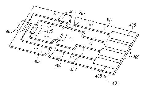
Figure 4 illustrates a simple biosensor 401 useful for illustrating the laser
ablation process
of the present invention, including a substrate 402 having formed thereon
conductive
to material 403 defining electrode systems comprising a first electrode set
404 and a second
electrode set 405, and corresponding traces 406, 407 and contact pads 408,
409,
respectively. Note that the biosensor 401 is used herein for purposes of
illustrating the
laser ablation process, and that it is not shown as incorporating the sense
lines of the
present invention. The conductive material 403 may contain pure metals or
alloys, or other
materials, which are metallic conductors. Preferably, the conductive material
is absorptive
at the wavelength of the laser used to form the electrodes and of a thickness
amenable to
rapid and precise processing. Non-limiting examples include aluminum, carbon,
copper,
chromium, gold, indium tin oxide (ITO), palladium, platinum, silver, tin
oxide/gold,
titanium, mixtures thereof, and alloys or metallic compounds of these
elements.
Preferably, the conductive material includes noble metals or alloys or their
oxides. Most
preferably, the conductive material includes gold, palladium, aluminum,
titanium,
platinum, ITO and chromium. The conductive material ranges in thickness from
about
10 nm to 80 nm, more preferably, 30 nm to 70 nm, and most preferably 50 nm. It
is
appreciated that the thickness of the conductive material depends upon the
transmissive
property of the material and other factors relating to use of the biosensor.
While not illustrated, it is appreciated that the resulting patterned
conductive material can
be coated or plated with additional metal layers. For example, the conductive
material may
be copper, which is then ablated with a laser into an electrode pattern;
subsequently, the
copper may be plated with a titanium/tungsten layer, and then a gold layer, to
form the
desired electrodes. Preferably, a single layer of conductive material is used,
which lies on
the base 402. Although not generally necessary, it is possible to enhance
adhesion of the
conductive material to the base, as is well known in the art, by using see
11
CA 2984221 2017-10-27
d or ancillary layers such as chromium nickel or titanium. In preferred
embodiments,
biosensor 401 has a single layer of gold, palladium, platinum or ITO.
Biosensor 401 is illustratively manufactured using two apparatuses 10, 10',
shown in
Figures 5, 6 and 7, respectively. It is appreciated that unless otherwise
described, the
apparatuses 410, 410' operate in a similar manner. Referring first to Figure
5, biosensor
401 is manufactured by feeding a roll of ribbon 420 having an 80 nm gold
laminate, which
is about 40 mm in width, into a custom fit broad field laser ablation
apparatus 410. The
apparatus 410 comprises a laser source 411 producing a beam of laser light
412, a
chromium-plated quartz mask 414, and optics 416. It is appreciated that while
the
illustrated optics 416 is a single lens, optics 416 is preferably a variety of
lenses that
cooperate to make the light 412 in a pre-determined shape.
A non-limiting example of a suitable ablation apparatus 410 (Figures 5-6) is a
customized
MicrolineLaser 200-4 laser system commercially available from LPKF Laser
Electronic
GmbH, of Garbsen, Germany, which incorporates an LPX-400, LPX-300 or LPX-200
laser
system commercially available from Lambda Physik AG, Gottingen, Germany and a
chromium-plated quartz mask commercially available from International
Phototool
Company, Colorado Springs, Co.
For the MicrolineLaser 200-4 laser system (Figures 5-6), the laser source 411
is a LPX-200
KrF-UV-laser. It is appreciated, however, that higher wavelength UV lasers can
be used in
accordance with this disclosure. The laser source 411 works at 248nm, with a
pulse energy
of 600mJ, and a pulse repeat frequency of 50 Hz. The intensity of the laser
beam 412 can
be infinitely adjusted between 3% and 92% by a dielectric beam attenuator (not
shown).
The beam profile is 27x15mm2 (0.62 sq. inch) and the pulse duration 25ns. The
layout on
the mask 414 is homogeneously projected by an optical elements beam expander,
homogenizer, and field lens (not shown). The performance of the homogenizer
has been
determined by measuring the energy profile. The imaging optics 416 transfer
the structures
of the mask 414 onto the ribbon 420. The imaging ratio is 2:1 to allow a large
area to be
removed on the one hand, but to keep the energy density below the ablation
point of the
applied chromium mask on the other hand. While an imaging of 2:1 is
illustrated, it is
appreciated that the any number of alternative ratios are possible in
accordance with this
12
CA 2984221 2017-10-27
disclosure depending upon the desired design requirements. The ribbon 420
moves as
shown by arrow 425 to allow a number of layout segments to be ablated in
succession.
The positioning of the mask 414, movement of the ribbon 420, and laser energy
are
computer controlled. As shown in Figure 5, the laser beam 412 is projected
onto the
ribbon 420 to be ablated. Light 412 passing through the clear areas or windows
418 of the
mask 414 ablates the metal from the ribbon 420. Chromium coated areas 424 of
the mask
414 blocks the laser light 412 and prevent ablation in those areas, resulting
in a metallized
structure on the ribbon 420 surface. Referring now to Figure 6, a complete
structure of
electrical components may require additional ablation steps through a second
mask 414'.
It is appreciated that depending upon the optics and the size of the
electrical component to
be ablated, that only a single ablation step or greater than two ablation
steps may be
necessary in accordance with this disclosure. Further, it is appreciated that
instead of
multiple masks, that multiple fields may be formed on the same mask in
accordance with
this disclosure.
Specifically, a second non-limiting example of a suitable ablation apparatus
410' (Figure
7) is a customized laser system commercially available from LPKF Laser
Electronic
GmbH, of Garbsen, Germany, which incorporates a Lambda STEEL (Stable energy
eximer
laser) laser system commercially available from Lambda Physik AG, Gottingen,
Germany
and a chromium-plated quartz mask commercially available from International
Phototool
Company, Colorado Springs, Co. The laser system features up to 1000 mJ pulse
energy at
a wavelength of 308 nm. Further, the laser system has a frequency of 100 Hz.
The
apparatus 410' may be formed to produce biosensors with two passes as shown in
Figures
5 and 6, but preferably its optics permit the formation of a 10x40 mm pattern
in a 25 ns
single pass.
While not wishing to be bound to a specific theory, it is believed that the
laser pulse or
beam 412 that passes through the mask 414, 414', 414" is absorbed within less
than 1 !AM
of the surface 402 on the ribbon 420. The photons of the beam 412 have an
energy
sufficient to cause photo-dissociation and the rapid breaking of chemical
bonds at the
metal/polymer interface. It is believed that this rapid chemical bond breaking
causes a
sudden pressure increase within the absorption region and forces material
(metal film 403)
to be ejected from the polymer base surface. Since typical pulse durations are
around 20-
13
CA 2984221 2017-10-27
25 nanoseconds, the interaction with the material occurs very rapidly and
thermal damage
to edges of the conductive material 403 and surrounding structures is
minimized. The
resulting edges of the electrical components have high edge quality and
accurate placement
as contemplated by the present invention.
Fluence energies used to remove or ablate metals from the ribbon 420 are
dependent upon
the material from which the ribbon 420 is formed, adhesion of the metal film
to the base
material, the thickness of the metal film, and possibly the process used to
place the film on
the base material, i.e. supporting and vapor deposition. Fluence levels for
gold on
KALADEX range from about 50 to about 90 mJ/cm2, on polyimide about 100 to
about
120 mJ/cm2, and on MELINEX about 60 to about 120 mJ/cm2. It is understood
that
fluence levels less than or greater than the above mentioned can be
appropriate for other
base materials in accordance with the disclosure.
Patterning of areas of the ribbon 420 is achieved by using the masks 414,
414'. Each mask
414, 414' illustratively includes a mask field 422 containing a precise two-
dimensional
illustration of a pre-determined portion of the electrode component patterns
to be formed.
Figure 5 illustrates the mask field 422 including contact pads and a portion
of traces. As
shown in Figure 6, the second mask 414' contains a second corresponding
portion of the
traces and the electrode patterns containing fingers. As previously described,
it is
appreciated that depending upon the size of the area to be ablated, the mask
414 can
contain a complete illustration of the electrode patterns (Figure 7), or
portions of patterns
different from those illustrated in Figures 5 and 6 in accordance with this
disclosure.
Preferably, it is contemplated that in one aspect of the present invention,
the entire pattern
of the electrical components on the test strip are laser ablated at one time,
i.e., the broad
field encompasses the entire size of the test strip (Figure 7). In the
alternative, and as
illustrated in Figures 5 and 6, portions of the entire biosensor are done
successively.
While mask 414 will be discussed hereafter, it is appreciated that unless
indicated
otherwise, the discussion will apply to masks 414', 414" as well. Referring to
Figure 5,
areas 424 of the mask field 422 protected by the chrome will block the
projection of the
laser beam 412 to the ribbon 420. Clear areas or windows 418 in the mask field
422 allow
the laser beam 412 to pass through the mask 414 and to impact predetermined
areas of the
14
CA 2984221 2017-10-27
ribbon 420. As shown in Figure 5, the clear area 418 of the mask field 422
corresponds to
the areas of the ribbon 420 from which the conductive material 403 is to be
removed.
Further, the mask field 422 has a length shown by line 430 and a width as
shown by line
432. Given the imaging ratio of 2:1 of the LPX-200, it is appreciated that the
length 30 of
the mask is two times the length of a length 434 of the resulting pattern and
the width 432
of the mask is two times the width of a width 436 of the resulting pattern on
ribbon 420.
The optics 416 reduces the size of laser beam 412 that strikes the ribbon 420.
It is
appreciated that the relative dimensions of the mask field 422 and the
resulting pattern can
to vary in accordance with this disclosure. Mask 414' (Figure 6) is used to
complete the two-
dimensional illustration of the electrical components.
Continuing to refer to Figure 5, in the laser ablation apparatus 410 the
excimer laser source
411 emits beam 412, which passes through the chrome-on-quartz mask 414. The
mask
field 422 causes parts of the laser beam 412 to be reflected while allowing
other parts of
the beam to pass through, creating a pattern on the gold film where impacted
by the laser
beam 412. It is appreciated that ribbon 420 can be stationary relative to
apparatus 410 or
move continuously on a roll through apparatus 410. Accordingly, non-limiting
rates of
movement of the ribbon 420 can be from about 0 m/min to about 100 m/min, more
preferably about 30 m/min to about 60 m/min. It is appreciated that the rate
of movement
of the ribbon 420 is limited only by the apparatus 410 selected and may well
exceed 100
m/min depending upon the pulse duration of the laser source 411 in accordance
with the
present disclosure.
Once the pattern of the mask 414 is created on the ribbon 420, the ribbon is
rewound and
fed through the apparatus 410 again, with mask 414' (Figure 6). It is
appreciated, that
alternatively, laser apparatus 410 could be positioned in series in accordance
with this
disclosure. Thus, by using masks 414, 414', large areas of the ribbon 420 can
be patterned
using step-and-repeat processes involving multiple mask fields 422 in the same
mask area
to enable the economical creation of intricate electrode patterns and other
electrical
components on a substrate of the base, the precise edges of the electrode
components, and
the removal of greater amounts of the metallic film from the base material.
CA 2984221 2017-10-27
The second embodiment of the present invention illustrated in FIGs. 8 and 9
improve upon
the prior art by providing for I-R drop compensation of both the working and
counter
electrode leads on the test strip. Referring now to FIG. 8, there is
schematically illustrated
a second embodiment test strip configuration of the present invention,
indicated generally
at 800. The test strip 800 comprises a bottom substrate 12 coated on its top
surface with a
50 nm conductive gold layer (for instance by sputtering or vapor deposition,
by way of
non-limiting example). Electrodes, connecting traces and contact pads therefor
are then
patterned in the conductive layer by a laser ablation process as described
hereinabove. For
example, working 814a, working sense 826a, counter 216a, and counter sense
224a
electrodes may be formed as shown and coupled to respective measurement
contact pads
814b, 826b, 216b and 224b by means of respective traces 814c, 826c, 216c and
224c.
These contact pads 814b, 826b, 216b and 224b provide a conductive area upon
the test
strip 800 to be contacted by a connector contact of the test meter (not shown)
once the test
strip 800 is inserted into the test meter.
It will be appreciated that the test strip 800 of FIG. 8 is substantially
identical to the first
embodiment test strip 200 of FIG. 2, except for the addition of the working
sense electrode
826a, contact pad 826b, and trace 826c. Provision of the working sense line
826 allows the
test meter to compensate for any I-R drop caused by the contact resistance of
the
connections to the contact pads 814b and 216b, and to compensate for the trace
resistance
of traces 814c and 216c.
Referring now to FIG. 9, there is shown a schematic electrical circuit diagram
of a second
embodiment electrode compensation circuit (indicated generally at 900) housed
within the
test meter. As indicated, the circuit couples to contact pads 826b, 814b, 216b
and 224b
when the test strip 800 is inserted into the test meter. As will be
appreciated by those
skilled in the art, a voltage potential is applied to the counter electrode
contact pad 216b,
which will produce a current between the counter electrode 216a and the
working electrode
814a that is proportional to the amount of analyte present in the biological
sample applied
to the reagent 18. The current from working electrode 814a is transmitted by
working
electrode trace 814c to working electrode contact pad 814b and provided to
current-to-
voltage amplifier 310. The analog output voltage of amplifier 310 is converted
to a digital
signal by A/D 312. This digital signal is then processed by microprocessor 314
according
to a previously stored program in order to determine the concentration of the
analyte of
16
CA 2984221 2017-10-27
interest within the biological sample applied to the test strip 800. This
concentration is
displayed to the user by means of LCD output device 316.
Microprocessor 314 also outputs a digital signal indicative of the voltage
potential to be
applied to the counter electrode contact pad 216b. This digital signal is
converted to an
analog voltage signal by D/A 318 (reference voltage source). The analog output
of D/A
318 is applied to a first input of an operational amplifier 320. A second
input of the
operational amplifier 320 is coupled to an output of operational amplifier
910. Operational
amplifier 910 is connected in a difference amplifier configuration using an
instrumentation
amplifier. A first input of operational amplifier 910 is coupled to working
sense electrode
contact pad 826b, while a second input of operational amplifier 910 is coupled
to counter
sense electrode contact pad 224b. The output of operational amplifier 320 is
coupled to the
counter electrode contact pad 216b. When the biosensor test strip (800) is
coupled to a test
meter a first input of the operational amplifier 910 operatively coupled to
the working
sense trace 826c and a second input is operatively coupled to the counter
sense trace 224c.
The output of the operational amplifier is operatively coupled to the counter
electrode
trace. The operational amplifier 910 in this configuration works as a
difference amplifier.
Operational amplifier 320 is connected in a voltage follower configuration, in
which the
amplifier will adjust its output (within its physical limits of operation)
until the voltage
appearing at its second input is equal to the commanded voltage appearing at
its first input.
Both inputs of operational amplifier 910 are high impedance inputs, therefore
substantially
no current flows in counter sense line 224 or working sense line 826. Since
substantially
no current flows, any parasitic resistance in counter sense line 224 or
working sense line
826 will not cause a potential drop, and the voltage appearing across the
inputs of
operational amplifier 910 is substantially the same as the voltage across the
measurement
cell (i.e. across counter electrode 216a and working electrode 814a). Because
operational
amplifier 910 is connected in a difference amplifier configuration, its output
represents the
voltage across the measurement cell.
Operational amplifier 320 will therefore act to vary its output (i.e. the
voltage potential
applied to the counter electrode contact pad 216b) until the actual voltage
potential
appearing across the measurement cell is equal to the voltage potential
commanded by the
microprocessor 314. Operational amplifier 320 therefore automatically
compensates for
17
CA 2984221 2017-10-27
any potential drop caused by the parasitic resistance in the counter electrode
trace 216c,
counter electrode contact 216b, working electrode trace 814c, and working
electrode
contact 814b, and therefore the potential appearing across the measurement
cell is the
desired potential. The calculation of the analyte concentration in the
biological sample
from the current produced by the working electrode is therefore made more
accurate.
FIG. 10, in conjunction with FIG. 8, illustrates a third embodiment of the
present invention
that improves over the prior art by providing I-R drop compensation for both
the working
and counter electrode lines, as well as providing verification that the
resistance of both the
working and counter electrode lines is not above a predetermined threshold in
order to
assure that the test meter is able to compensate for the I-R drops. Referring
now to FIG.
10, there is shown a schematic electrical circuit diagram of a third
embodiment electrode
compensation circuit (indicated generally at 1000) housed within the test
meter. The
electrode compensation circuit 1000 works with the test strip 800 of FIG. 8.
As indicated,
the circuit couples to contact pads 826b, 814b, 216b and 224b when the test
strip 800 is
inserted into the test meter. As will be appreciated by those skilled in the
art, a voltage
potential is applied to the counter electrode contact pad 216b, which will
produce a current
between the counter electrode 216a and the working electrode 814a that is
proportional to
the amount of analyte present in the biological sample applied to the reagent
18. The
current from working electrode 814a is transmitted to working electrode
contact pad 814b
by working electrode trace 814c and provided to current-to-voltage amplifier
310. The
output of current-to-voltage amplifier 310 is applied to the input of
instrumentation
amplifier 1002 which is configured as a buffer having unity gain when switch
1004 in the
closed position. The analog output voltage of amplifier 1002 is converted to a
digital
signal by A/D 312. This digital signal is then processed by microprocessor 314
according
to a previously stored program in order to determine the concentration of
analyte within the
biological sample applied to the test strip 800. This concentration is
displayed to the user
by means of LCD output device 316.
Microprocessor 314 also outputs a digital signal indicative of the voltage
potential to be
applied to the counter electrode contact pad 216b. This digital signal is
converted to an
analog voltage signal by D/A 318. The analog output of D/A 318 is applied to
the input of
an operational amplifier 320 that is configured as a voltage follower when
switch 1006 is
in the position shown. The output of operational amplifier 320 is coupled to
the counter
18
CA 2984221 2017-10-27
electrode contact pad 216b, which will allow measurement of a biological fluid
sample
applied to the reagent 18. Furthermore, with switches 1006, 1008 and 1010
positioned as
illustrated in FIG. 10, the circuit is configured as shown in FIG. 9 and may
be used to
automatically compensate for parasitic and contact resistance as described
hereinabove
with respect to FIG. 9.
In order to measure the amount of parasitic resistance in the counter
electrode line 216,
switch 1008 is placed in the position shown in FIG. 10, switch 1006 is placed
in the
position opposite that shown in FIG. 10, while switch 1010 is closed. The
operational
amplifier 320 therefore acts as a buffer with unity gain and applies a voltage
potential to
counter electrode contact pad 216b through a known resistance Rnom. This
resistance
causes a current to flow in the counter electrode line 216 and the counter
sense line 224
that is sensed by current-to-voltage amplifier 310, which is now coupled to
the current
sense line through switch 1010. The output of current-to-voltage amplifier 310
is provided
to the microprocessor 314 through AID 312. Because the value of Rnom is known,
the
microprocessor 314 can calculate the value of any parasitic resistance in the
counter sense
line 224 and the counter electrode line 216. This
parasitic resistance value can be
compared to a predetermined threshold stored in the test meter to determine if
physical
damage has occurred to the test strip 800 or if nonconductive buildup is
present on the
contact pads to such an extent that the test strip 800 cannot be reliably used
to perform a
test. In such situations, the test meter may be programmed to inform the user
that an
alternate test strip should be inserted into the test meter before proceeding
with the test.
In order to measure the amount of parasitic resistance in the working
electrode line 814,
switches 1006 and 1008 are placed in the position opposite that shown in FIG.
10, while
switch 1010 is opened. The operational amplifier 320 therefore acts as a
buffer with unity
gain and applies a voltage potential to working sense contact pad 826b through
a known
resistance Rnom. This resistance causes a current to flow in the working sense
line 826
and the working electrode line 814 that is sensed by current-to-voltage
amplifier 310. The
output of current-to-voltage amplifier 310 is provided to the microprocessor
314 through
A/D 312. Because the value of Rnom is known, the microprocessor 314 can
calculate the
value of any parasitic resistance in the working sense line 826 and the
working electrode
line 814. This parasitic resistance value can be compared to a predetermined
threshold
stored in the test meter to determine if physical damage has occurred to the
test strip 800 or
19
CA 2984221 2017-10-27
if nonconductive buildup is present on the contact pads to such an extent that
the test strip
800 cannot be reliably used to perform a test. In such situations, the test
meter may be
programmed to inform the user that an alternate test strip should be inserted
into the test
meter before proceeding with the test.
While the invention has been illustrated and described in detail in the
drawings and
foregoing description, the description is to be considered as illustrative and
not restrictive
in character. Only the preferred embodiment, and certain other embodiments
deemed
helpful in further explaining how to make or use the preferred embodiment,
have been
shown. All changes and modifications that come within the spirit of the
invention are
desired to be protected.
CA 2984221 2017-10-27