Note : Les descriptions sont présentées dans la langue officielle dans laquelle elles ont été soumises.
CA 02986140 2017-11-15
WO 2016/187300 PCT/US2016/033077
TITLE
ELECTRON PARAMAGNETIC RESONANCE (EPR) SYSTEMS WITH ACTIVE CANCELLATION
RELATED APPLICATIONS
[0001] This application claims the benefit of U.S. Provisional Patent
Application No. 62/163,042
filed on May 18, 2015, which is incorporated herein by reference.
FIELD OF THE INVENTION
[0002] This invention relates to Electron Paramagnetic Resonance (EPR)
systems. More
particularly, to an active cancellation structure for EPR systems.
BACKGROUND OF INVENTION
[0003] Interference-resilient transceivers, where the receiver (RX) is able to
operate without
performance degradation under a large interference power, are often required
in many
applications including full-duplex wireless communication, magnetic resonance
and dielectric
spectroscopy, and full-duplex radar. Existing interference-resilient
transceivers can be
characterized into two categories: (1) Reject the interference at IF with
little voltage gain at RF
(mixer-first). (2) Reject the interference at RF using a high-Q filter.
Unfortunately, method 1
suffers from large 1/f noise contributed by mixers and baseband circuitries at
low IF due to the
lack of voltage gain at RF. While method 2 has a low interference P ldB when
the frequency
offset between the interference and desired RX signal is small due to the low
quality factor of the
RF filter. Thus, method 2 is limited by the filter quality factor.
[0004] Recently, Electron Paramagnetic Resonance (EPR) spectroscopy has
attracted great
interest from both academia and industry. It is in concept highly similar to
nuclear magnetic
resonance (NMR), except that EPR spectroscopy detects magnetic moments
generated by
unpaired electrons instead of nucleus. EPR spectroscopy has a broad range of
applications, such
1
CA 02986140 2017-11-15
WO 2016/187300 PCT/US2016/033077
as discussed in WO 2015/048249 filed Sept. 25, 2014, US2014/0091802 filed
Sept. 30, 2013,
and 2014/0097842 filed Sept. 30, 2013.
[0005] In EPR spectroscopy, there is a desire for low NF at low IF. TX and RX
may operate at
the same time, where TX operates at fTx of several to tens of GHz. TX leakage
power may easily
reach -10dBm. RX may operate at fTx fm, where fm is tens of kHz. The
interference is caused
by the power leakage from the transmitter (TX) (self-interference), which may
operate at GHz
frequencies, and can easily reach -10dBm. Moreover, the frequency offset
between the TX and
the desired RX signal, as well as the frequency of the IF signal, may be less
than 100kHz. Under
such stringent conditions, existing interference-resilient architectures
cannot satisfy both noise
and linearity requirements, simultaneously. As a result, conventional high-
performance EPR
spectrometers may separate the TX and RX into dedicated discrete components
that are bulky
and costly.
[0006] An active cancellation structure is discussed herein that improves
sensitivity of EPR
systems or the like.
2
CA 02986140 2017-11-15
WO 2016/187300 PCT/US2016/033077
SUMMARY OF INVENTION
[0007] In one embodiment, an active cancellation system may be utilized to
cancel interference,
such as from transmitter leakage or self-interference in a transceiver of an
electron paramagnetic
resonance (EPR) spectrometer. The active cancellation system may be inserted
between the
transmitter and receiver. The active cancellation system may receive the
output of the
transmitter, and generate a cancellation signal with the same amplitude, but
1800 phase shifted
relative to the self-interference signal. The cancellation system may include
an attenuator/
amplitude tuner, buffer, and phase shifter. In some embodiments, the
cancellation system may
further include an I/Q generator and the phase shifter may be a Cartesian
phase shifter.
[0008] In yet another embodiment, an active cancellation method may include
receiving an
output signal from a transmitter, and attenuating/amplitude tuning the signal.
The signal may
then be sent to a buffer, which may further tune the amplitude of the signal
in some
embodiments. The signal may be converted into a phase shifted 180 relative to
the self-
interference signal, and subsequently combined to provide a cancellation
signal that can be
provided to a receiver to mitigate or eliminate self-interference. In some
embodiments, the
method may also include converting a differential signal into a quadrature
signal, which is later
combined after proper weighting of I and Q to produce the cancellation signal.
[0009] The foregoing has outlined rather broadly various features of the
present disclosure in
order that the detailed description that follows may be better understood.
Additional features and
advantages of the disclosure will be described hereinafter.
3
CA 02986140 2017-11-15
WO 2016/187300 PCT/US2016/033077
BRIEF DESCRIPTION OF THE DRAWINGS
[0010] For a more complete understanding of the present disclosure, and the
advantages thereof,
reference is now made to the following descriptions to be taken in conjunction
with the
accompanying drawings describing specific embodiments of the disclosure,
wherein:
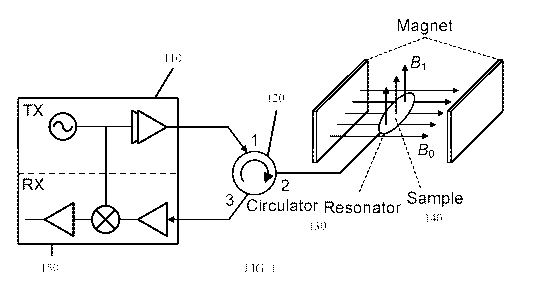
[0011] FIG. 1 shows the architecture of an absorption-power-based EPR
spectrometer;
[0012] FIG. 2 shows an illustrative embodiment of a transceiver architecture
providing self-
interference cancellation;
[0013] FIG. 3 presents the schematic of a self-interference cancellation
circuit;
[0014] FIGS. 4(a)-4(c) respectively show a simple capacitor divider, inductor-
assisted capacitor
divider with an ideal inductor, and inductor-assisted capacitor divider with a
real inductor;
[0015] FIGS. 5(a)-5(b) respectively show simulation results for the dividing
ratio under different
inductor Q, and simulation results for the phase shift of the divider output
under different
inductor Q;
[0016] FIG. 6 shows simulated noise power at the LNA output and the
cancellation circuit
output when the cancellation circuit gain is set at the maximum value;
[0017] FIGS. 7(a)-7(b) respectively show schematic of a VCO and a current-mode
logic (CML)
frequency divider;
[0018] FIG. 8 shows a schematic of a power amplifier (PA);
[0019] FIG. 9 shows a schematic of a receiver (RX) front end;
[0020] FIG. 10 shows a schematic of baseband amplifiers;
[0021] FIG. 11 shows a micrograph of a fabricated chip;
[0022] FIG. 12 shows measurement results for the VCO tuning range;
[0023] FIG. 13 shows measured TX output power versus frequency;
4
CA 02986140 2017-11-15
WO 2016/187300 PCT/US2016/033077
[0024] FIGS. 14(a)-14(b) respectively show measured self-interference
cancellation under
different interference power and phase, and measured self-interference
cancellation under
different frequencies;
[0025] FIG. 15 shows measurement results for the RX conversion gain;
[0026] FIG. 16 shows measurement results for the RX NF under various
conditions;
[0027] FIGS. 17(a)-17(b) respectively show the signal spectrum measured at the
monitoring
node under a TX leakage of -20dBm and plot of the conversion gain of the RX at
various TX
leakage power levels;
[0028] FIGS. 18(a)-18(c) show the principles of the magnetic field-sweep and
the frequency-
sweep methods in EPR spectroscopy;
[0029] FIGS. 19(a)-19(b) show measured EPR response from DPPH powder sample in
(a) log
scale and (b) linear scale using the Bo-sweep method;
[0030] FIGS. 20(a)-20(b) measured EPR response for DPPH power using the
frequency sweep
method in (c) linear scale and (d) log scale;
[0031] FIGS. 21(a)-21(b) respectively show the measured EPR response of MgO-Cr
+ crystal in
the linear scale and log scale using the Bo-sweep method;
[0032] FIGS. 21(c)-21(d) respectively show the measured EPR response of 63mg
Fe304
nanoparticles in the linear scale and log scale using the Bo-sweep method; and
[0033] FIG. 22 shows EPR recorder voltage v. current for several trials.
CA 02986140 2017-11-15
WO 2016/187300 PCT/US2016/033077
DETAILED DESCRIPTION
[0034] Refer now to the drawings wherein depicted elements are not necessarily
shown to scale
and wherein like or similar elements are designated by the same reference
numeral through the
several views.
[0035] Referring to the drawings in general, it will be understood that the
illustrations are for the
purpose of describing particular implementations of the disclosure and are not
intended to be
limiting thereto. While most of the terms used herein will be recognizable to
those of ordinary
skill in the art, it should be understood that when not explicitly defined,
terms should be
interpreted as adopting a meaning presently accepted by those of ordinary
skill in the art.
[0036] It is to be understood that both the foregoing general description and
the following
detailed description are exemplary and explanatory only, and are not
restrictive of the invention,
as claimed. In this application, the use of the singular includes the plural,
the word "a" or "an"
means "at least one", and the use of "or" means "and/or", unless specifically
stated otherwise.
Furthermore, the use of the term "including", as well as other forms, such as
"includes" and
"included", is not limiting. Also, terms such as "element" or "component"
encompass both
elements or components comprising one unit and elements or components that
comprise more
than one unit unless specifically stated otherwise.
[0037] Transceivers have many applications, but in some cases, interference
resulting from
transmitter (TX) leakage (or self-interference) may cause signal accuracy
issues for such
applications. As the transmitted signal is generally known, it is possible to
generate a cancelation
signal in accordance with the known transmitted signal and cancel the
interference at RF.
[0038] An electron paramagnetic resonance (EPR) spectrometer is the equipment
that measures
the EPR response of a sample. Continuous-wave absorption-power-based EPR
spectrometer are
6
CA 02986140 2017-11-15
WO 2016/187300 PCT/US2016/033077
the most widely-used type of EPR spectrometer and are discussed herein. Figure
1 shows the
architecture of an absorption-power-based EPR spectrometer. During the
measurement, the
transmitter (TX) 110 delivers a microwave signal through circulator 120 to the
resonator 130,
which contains the sample 140. The resonator generates a strong
electromagnetic field B1, which
interacts with the sample and excites electron transition. The static magnetic
field Bo is gradually
swept, but the frequency and power of the TX signal is fixed. When EPR occurs,
a portion of the
electromagnetic energy is absorbed by the sample, altering the reflected
microwave power from
the resonator 130. The receiver (RX) 150 receives the reflected power, down-
converts it to
baseband, and monitors the change. To reduce the effects of low-frequency
noise, the static field
Bo is modulated. The frequency of the received signal at the baseband output
of the RX 150 is the
same as the modulation frequency. Theoretically, to maximize the sensitivity
of the system, the
modulation frequency should be much higher than the flicker noise corner of
the RX 150.
Unfortunately, due to limitations, such as the difficulty of generating a
strong high-frequency
magnetic field, the modulation frequency in current EPR spectrometers rarely
exceeds 100kHz.
This poses a stringent requirement on the RX NF at low baseband frequencies.
[0039] In an absorption-power-based EPR spectrometer, the minimally-detectable
number of
electron spins is proportional to the square root of the RX noise factor and
inversely-proportional
to the TX output power. Unfortunately, low RX NF and large TX output power
cannot be
simultaneously satisfied using single-chip-transceiver-based EPR
spectrometers. This is caused
by the TX self-interference signal present at the RX input. During the
operation of an EPR
spectrometer, a small portion of the TX signal, denoted as TX self-
interference, always couples
to the RX input through two major coupling mechanisms: 1) the finite isolation
value of the
circulator, and 2) the reflection from the resonator due to non-perfect
matching. As an example,
7
CA 02986140 2017-11-15
WO 2016/187300 PCT/US2016/033077
the typical amplitude of the TX self-interference signal is lower than the TX
output power (e.g.
¨30dB). Its frequency only deviates from the RX frequency by the modulation
frequency of the
Bo field, which is no more than 100kHz in the nonlimiting examples discussed.
Because the
frequency of the TX self-interference and EPR signals deviate by only a small
amount, it is
extremely challenging to remove the TX self-interference signal before down-
conversion by a
filter. As indicated before, the baseband frequency for an EPR spectrometer is
the same as the
modulation frequency of the magnetic field Bo. At such low frequencies, the
flicker noise of
mixers and baseband amplifiers can contribute significantly to the RX NF, if
it is not suppressed
by a strong voltage amplification before down-conversion. However, if the TX
is generating a
strong output signal, the TX self-interference would be excessively large at
the RX input,
saturating the RX and preventing a large voltage gain. As a result, a large TX
output power and
a low RX NF cannot be simultaneously achieved without using the improved
architecture
discussed herein. While some techniques have been proposed for mitigating the
TX self-
interference in an in-band full-duplex transceiver as discussed previously,
they provide poor NF
at low baseband frequencies.
[0040] The following discussion of a transceiver with active self-interference
cancellation
includes discussion of examples to demonstrate particular aspects of the
present disclosure. It
should be appreciated by those of ordinary skill in the art that the methods
and parameters
described in the examples that follow merely represent illustrative
embodiments of the
disclosure. Those of ordinary skill in the art should, in light of the present
disclosure, appreciate
that many changes can be made in the specific embodiments described and still
obtain a like or
similar result without departing from the spirit and scope of the present
disclosure. While
nonlimiting examples discussed herein are directed towards EPR spectrometers,
the claims are
8
CA 02986140 2017-11-15
WO 2016/187300 PCT/US2016/033077
not limited to use with EPR spectrometers except where explicitly stated.
[0041] Transceiver Architecture
[0042] A transceiver with active self-interference cancellation is discussed
herein. In order to
improve the sensitivity of the EPR spectrometer, integration of a cancellation
circuit on the
transceiver chip is proposed to mitigate the TX self-interference. In EPR
spectroscopy, the
sensitivity of the system increases with the operation frequency, thereby
making it desirable to
have a high operation frequency. Figure 2 shows an illustrative embodiment of
a transceiver
architecture providing self-interference cancellation. In some embodiments,
the transceiver may
provide TX 210 and RX 250 on the same chip. In other embodiments, the TX 210
and RX 250
may be separated. In some embodiments, the transceiver may be utilized for EPR
spectroscopy.
The TX 210 may provide a voltage controlled oscillator (VCO) 220, divider 230,
and
amplifier(s) 240 utilized to produce a desired output. In order to cancel the
TX self-interference
signal or leakage, an on-chip self-interference cancellation circuit 215 is
inserted between the TX
210 and the RX 250. The cancellation circuit 215 takes the TX output 225 as
its input. A
cancellation signal 235 should have the same amplitude as the TX self-
interference signal or
leakage, but should be shifted 180 phase shift to properly cancel the
interference. Ideally, a
cancellation signal has an identical amplitude to and shifted exactly 180
from the TX self-
interference signal so that it will perfectly cancel the interference signal.
However, a variance of
5% from the amplitude or 180 phase shift may be sufficient for substantial
cancellation of the
interference signal, and considered to be approximately equal amplitude or 180
. One the
cancellation signal 235 has been phase shifted it can be provided to the input
of the receiver 245
to cancel the TX self-interference signal. In order to achieve a low RX NF,
the noise penalty
from the self-interference cancellation circuit must be minimized. Toward this
purpose, the
9
CA 02986140 2017-11-15
WO 2016/187300 PCT/US2016/033077
cancellation signal is injected after the Low-Noise Amplifier (LNA) 255,
instead of at the RX
input. By carefully choosing the gain of the LNA 255, the noise contribution
from the
cancellation circuit 215 can be suppressed, while the RX still maintains good
linearity.
[0043] After the TX self-interference signal is removed from the RX, the
desired EPR signal is
further amplified by amplifier 265 and then down-converted to baseband. At the
baseband input,
a DC offset filtering block 275 is used to reject the DC offset. In some
embodiments, because the
baseband signal in EPR spectroscopy is typically on the order of tens of kHz,
external 10i.tF
capacitors may be utilized in the DC offset filtering block 275. After
filtering, the remaining
EPR signal is further amplified by baseband amplifiers 285 and delivered to an
off-chip data-
acquisition unit for processing. Further details of the transceiver
architecture are discussed
below with respect to drawings providing additional details of the
architecture.
[0044] Self-Interference Cancellation Circuit
[0045] The self-interference cancellation circuit may generate a cancellation
signal with tunable
phase and amplitude to cancel the interference signal. No assumptions have
been made on the
phase of the interference signal so the cancellation circuit is required to
have 360 phase
tunability. As a nonlimiting example, the amplitude of the TX self-
interference signal is assumed
to have a maximum value of approximately -10dBm, considering 20dBm TX output
power and a
30dB TX-RX isolation. As introduced before, the cancellation signal is
injected into RX after the
EPR signal has been amplified by a LNA, whose gain is designed to be
approximately 10dB in
the experimentation. Therefore, the maximum amplitude of the cancellation
signal is required to
exceed OdBm. Moreover, it is desirable that the cancellation signal has at
least 15dB of
amplitude tunability so that a relatively weak self-interference signal can be
cancelled as well.
[0046] Figure 3 presents the schematic of the self-interference cancellation
circuit, which may be
CA 02986140 2017-11-15
WO 2016/187300 PCT/US2016/033077
part of an EPR spectrometer such as shown previously in figure 2. The
cancellation circuit may
receive an output 310 (e.g. PA output) from a transmitter, thereby essentially
sampling the signal
that is to be cancelled. Because the TX output may exceed a certain decibel-
milliwatts level (e.g.
20dBm), the PA output 310 (e.g. from amplifier 240) may be attenuated and
amplitude tuned by
an attenuator/amplitude tuner 320 before outputting the signal or cancellation
signal to the
remainder of the cancellation circuit; otherwise, the active devices in the
cancellation circuit may
face severe reliability/breakdown concerns. In some embodiments, the
attenuator at the input of
the cancellation circuit may be realized through a voltage divider or through
an active circuit or
device. In some embodiments, the active circuit or device may have a gain of
smaller than 1 to
increase the isolation between the output and input. As a nonlimiting example,
the active circuit
may be transistor based. In order to reduce the noise from the self-
interference cancellation
circuit, the amplitude tuner may be merged with the attenuator (or herein
attenuator/amplitude
tuner 320). An extra stage to perform amplitude tuning for the cancellation
signal can be
utilized, but the merged attenuator/amplitude tuner 320 is preferred. Two
varactors (e.g. reverse-
biased diode varactors) are merged with the voltage divider and used to
perform the amplitude
tuning to minimize the added thermal noise. A resistor divider could be
utilized, but the two
reverse-biased diode varactors are preferred. By changing the capacitance of
the varactors, the
dividing ratio is varied. In a divider containing only two capacitors Ci and
C2, as shown in
Figure 4(a), if the varactor capacitance Ci can be increased by Nx, without
considering the load
impedance, the amplitude tuning range of the divider output is
Ncl +c2
(1)
cl + c2
[0047] To achieve a large amplitude tuning range of the divider output, the
tuning range of the
11
CA 02986140 2017-11-15
WO 2016/187300 PCT/US2016/033077
varactor capacitance should be maximized. Unfortunately, in the process where
the proposed
transceiver is implemented, the tuning range of the varactor capacitance is
limited to
approximately 2-3x. Therefore, the amplitude tunability of the divider output
is restricted to
10dB or less. This number could be further reduced if the load impedance is
considered. In order
to enlarge the amplitude tuning range of the divider output, a parallel LC
resonance network is
used to increase the tuning range for the effective capacitance of the
varactor. As shown in
Figure 4(b), if an inductor is connected in parallel to the varactor, the
admittance of the network
becomes
(2)
If the value of L and C1 are chosen such that the admittance always has a
positive imaginary part,
the effective capacitance of this LC network would be
C =C1 ¨ ¨ (3)
f
Now the tuning range of Cuff is
(4)
By choosing Ci slightly larger than ,, the tuning range of Cuff could be
much larger than 3,
and thus the amplitude of the divider output could achieve a large tuning
range. Moreover,
because the admittance of the LC network is purely imaginary and remains
positive, the phase
shift of the voltage divider is constant across all the dividing ratios.
[0048] In reality, the quality factor of the inductor may limit the amplitude
tuning range of the
12
CA 02986140 2017-11-15
WO 2016/187300 PCT/US2016/033077
divider output. If the inductor has a quality factor of Q, the admittance of
the parallel LC
network is
= jwCi+ = jwC1 õ _______________________________________ (5)
L' (1 a42L' 4aLQ
Q"
Note that the effective capacitance remains the same, as in the case where the
inductor is ideal,
but the admittance now has a positive real part. The resulting tuning range of
the dividing ratio is
Lt2 (Cm+ Cef f ¨yr,ax)
(6)
Here Ceff_max and Ceff_min are the maximum and minimum values of Cuff. This
equation shows that,
for the same values of Cuff and C2, a lower inductor Q results in a lower
tuning range of the
dividing ratio. Moreover, the phase shift of the divider output would vary at
different dividing
ratios due to the finite inductor Q. Figures 5(a)-5(b) respectively plot the
simulation results for
the dividing ratio under different inductor Q and for the phase shift of the
output of the voltage
divider under different inductor Q. The simulation is performed at 4.5GHz. C2
is set at 200fF, the
inductance is chosen to be 0.8nH, and Ci is varied from 2pF to 5pF. As shown,
the inductor Q
should be maximized to achieve a larger tuning range of the divider ratio plus
a small variation
in the phase shift of the divider output. As a nonlimiting example
corresponding to experimental
example, with an inductor Q of 13, the divider output has a tuning range of
14dB, and the phase
shift across the entire tuning range is within 4 in simulation.
[0049] Returning to figure 3, a high input-impedance buffer 330 follows the
attenuator/amplitude tuner 320 and receives the signal from the tuner. The
input impedance of
the buffer 330 can be absorbed into the quality factor of the inductor when
analyzing the
performance of the voltage divider. Because the amplitude of the divider
output can still be large,
13
CA 02986140 2017-11-15
WO 2016/187300 PCT/US2016/033077
high breakdown transistors are used when constructing the buffer, such as
with, but not limited
to, high breakdown transistors (e.g. 10V or higher). To provide additional
tuning of the
amplitude of the cancellation signal, the load impedance of the buffer can be
varied. The signal
from the buffer 330, which has been amplitude tuned and attenuated, may be
provided to a phase
shifter 340. The phase shifter 340 receiving the signal may phase shift the
cancellation signal to
180 relative to the TX self-interference signal. The cancellation signal may
be outputted by the
phase shifter 340 to a receiver to cancel the interference caused by TX
leakage.
[0050] In some embodiments, the signal or cancellation signal may be a
differential signal. In
such embodiments, an I-Q generator 350 may follow the buffer and converts the
differential
signal into a quadrature signal. The quadrature signal is sent to a Cartesian
phase shifter 360,
which phase shifts and assigns different weights to the I and Q branches of
the quadrature signal
to provide proper weighting for the cancellation signal to cancel the self-
interference signal. I
can be regarded as a vector on the real axis and Q can be regarded as a vector
on the imaginary
axis. By proper weighting of I and Q, it is possible to generate any value on
the complex plane.
Subsequently, the I and Q branches are combined to form the cancellation
signal. The weights of
the I and Q signals are controlled by varying the gain of the two buffers 330
that amplify the
signal. The cancellation signal is finally injected into the RX through a
buffer.
[0051] An important criteria of the self-interference cancellation circuit is
that its noise
contribution must be small. To achieve this goal, voltage amplification in the
cancellation circuit
is mostly avoided, as any voltage gain will amplify the noise of the
cancellation circuit as well.
Figure 6 presents the simulation results of the noise contribution from the
cancellation circuit.
The simulation is performed when the gain of the cancellation circuit is set
at the maximum
value. At the LNA output, where the cancellation signal is injected to the RX,
the noise
14
CA 02986140 2017-11-15
WO 2016/187300 PCT/US2016/033077
introduced from the cancellation circuit is much smaller than the noise caused
by the LNA
(including the noise from the 500 LNA input and the noise produced by the
LNA). This
translates to a noise penalty of only 0.2dB.
[0052] Design of the TX and RX
[0053] Additional components of the EPR spectrometer shown in figure 2 are
discussed in
further detail herein. The TX signal is generated using a Voltage-Controlled
Oscillator (VCO)
220. The frequency of the VCO 220 may be designed to be twice the operation
frequency of the
EPR spectrometer. A frequency divider 230 then divides the frequency of the
VCO signal by
two, simultaneously providing I and Q signals that are necessary to generate
the LO signals for
the down-conversion mixer. Figures 7(a)-7(b) presents the schematic of the VCO
and the
frequency divider. The VCO takes a differential cross-coupled design. As a
nonlimiting example,
the VCO frequency is around 9GHz, The frequency divider uses a Current-Mode
Logic (CML)
structure, which is suitable for high-speed operation.
[0054] Returning to figure 2, following the frequency divider 230, an
amplifier chain or power
amplifier (PA) 240 amplifies the TX signal. The PA 240 finally delivers the
signal to a
differential pair of loads (e.g. 50S2). The schematic of the PA is shown in
Figure 8. The PA is
based on a class-AB design and is fully integrated on-chip. The simulated
input-referred ldB
compression point (P ldB) is 7dBm.
[0055] The detailed design of the RX front-end corresponding to the EPR
spectrometer in figure
2 is presented in figure 9. The first stage in the RX is an inductive-
degenerated cascode LNA
910. The load of the LNA 910 is shared with the buffer 920 of the self-
interference cancellation
circuit, which injects the cancellation signal at the LNA output. In order to
monitor the effects of
the self-interference cancellation, a voltage-monitoring buffer 930 is added
at the LNA output.
CA 02986140 2017-11-15
WO 2016/187300 PCT/US2016/033077
This buffer 930 senses the LNA output, attenuates it (e.g. 10dB), and then
sends it to output
pads. The monitor output of the monitoring buffer 930 is used to guide the
amplitude and the
phase tuning of the cancellation signal. A Gm cell buffer (CMOS part of 940)
amplifies the signal
further. After the TX self-interference signal has been removed from the RX,
the remaining EPR
signal is further amplified to suppress the flicker noise caused by mixers and
baseband
amplifiers. Referring to figure 2, the down-conversion is performed by a
current-mode passive
mixer 270. Compared to active mixers, the passive mixer 270 introduces a
smaller flicker noise.
Moreover, by minimizing the input impedance of the baseband Trans-Impedance
Amplifier
(TIA), a current-mode passive mixer 270 provides an improved linearity. This
is because the
large voltage swing, which causes device nonlinearities, is avoided in the
circuit. The LO signal
of the passive mixer is generated from the l/Q outputs of the frequency
divider following the
VCO (e.g. LO generator 280). The signal may have a 25% duty cycle, increasing
the mixer
conversion gain by 3dB, compared to a 50% duty cycle LO. The design of the Gm
cell (CMOS
part of 940) is also shown in figure 9. It is constructed using a class AB
CMOS cell. The Gm cell
has very high linearity. In simulation, the trans-conductance gain is only
reduced by ldB when
the input voltage swing reaches 1.4V.
[0056] The design of the baseband amplifiers is shown in figure 10. The
baseband TIA is
implemented using a common-base amplifier. The input impedance is kept small
(e.g., 100) to
increase the linearity of the Gm cell and the passive mixer. The signal is
finally amplified and
delivered off chip through a buffer (e.g. 500).
[0057] Transceiver measurement results
[0058] Figure 11 presents the micrograph of the reported transceiver. The
transceiver chip is
fabricated in IBM 0.13iim BiCMOS process technology. It occupies an area of
4.8mm by 2.5mm
16
CA 02986140 2017-11-15
WO 2016/187300 PCT/US2016/033077
and consumes 2W of DC power during the operation. Major blocks of the
transceiver are labeled
in the figure.
[0059] The measured frequency tunability of the TX signal is shown in figure
12. During this
measurement, the voltage of the tuning node of the on-chip VCO is varied, and
the frequency of
the frequency divider output is measured using an Agilent signal analyzer
N9030A. As shown in
the figure, the frequency of the signal can be varied from 3.8GHz to 5.2GHz.
[0060] The TX output power versus frequency is shown in figure 13. This power
is measured
after the differential TX outputs have been combined using an off-chip balun.
It is observed that
the TX can generate a maximum output power of 22dBm. The measured 3dB
bandwidth is 1GHz
(from 3.8GHz to 4.8GHz.).
[0061] The performance of the self-interference cancellation circuit is shown
in figures 14(a)-
14(b). The purpose of these measurements is to determine if the cancellation
circuit can cancel
the TX self-interference signal across a wide range of phase, amplitude, and
frequencies. During
this measurement, the TX output is connected to the RX input through an
external phase shifter
and a variable-gain attenuator. Therefore, the phase and amplitude of the self-
interference signal
can be externally controlled and varied. Moreover, the frequency of the self-
interference signal
can be controlled by varying the oscillation frequency of the on-chip VCO. As
the phase,
amplitude, and frequency of the TX self-interference signal are extensively
varied, the control
voltage of the on-chip self-interference cancellation circuit is changed to
cancel the self-
interference signal. As a proof-of-concept design, an external voltage supply
with a step voltage
of 0.01V provides the control voltages for the cancellation circuit. Figures
14(a)-14(b)
respectively show the measurement results for interference power (dBm) v.
phase (degrees) and
interference power cancellation (dB) v. frequency (GHz). Clearly, the TX self-
interference signal
17
CA 02986140 2017-11-15
WO 2016/187300 PCT/US2016/033077
can be cancelled by at least 32dB across a wide range of phases, amplitudes,
and frequencies.
[0062] The RX conversion gain and linearity are studied next in Figure 15. As
is shown in this
figure, the RX achieves a conversion gain of 46dB. If the self-interference
cancellation circuit is
turned off, the self-interference PldB is -20dBm. However, when the self-
interference
cancellation circuit is turned on and the TX self-interference signal is
cancelled, the self-
interference PldB increases to -8dBm. This demonstrates the effectiveness of
the self-
interference cancellation circuit.
[0063] Finally, the NF of the RX is studied. During the NF measurement, a
stable external RF
source is used to generate the TX and LO signals for the down-conversion
mixer. This improves
measurement accuracy, especially at low baseband frequencies. As shown in
Figure 16, when
both the TX and the cancellation circuit are turned off, the RX achieves a NF
of 3.1dB/6.3dB at
10MHz/50kHz baseband frequencies. When the TX remains off and the cancellation
circuit is
turned on and configured at the maximum gain settings, the cancellation
circuit incurs a noise
penalty of no more than 0.6dB across the baseband frequencies from 50kHz to
10MHz. When
the TX and cancellation circuit are turned on and the self-interference power
is -10dBm at the
RX input, the RX NF is 6.8dB/11.1dB at 10MHz/50kHzbaseband. The degradation in
the NF is
believed to be attributed to multiple factors, such as the increased noise of
the power supply and
ground rail caused by the TX. If the cancellation circuit is turned off under
the same self-
interference power, the RX NF is 12.4dB/20.7dB at 10MHz/50kHz baseband
frequencies. This
demonstrates that the self-interference cancellation circuit can improve the
NF significantly
when there is a strong TX self-interference signal at the RX input.
[0064] Table I provides a summary of the performance of an improved
transceiver. The reported
transceiver achieves the lowest NF, especially at low baseband frequencies.
The flicker noise
18
CA 02986140 2017-11-15
WO 2016/187300 PCT/US2016/033077
corner of the reported transceiver is 60kHz, more than one order of magnitude
lower than prior
works. Furthermore, the reported transceiver is the first work that
demonstrates the operation of
the in-band full-duplex RX and the associated self-interference cancellation
circuit when a co-
integrated TX is operating at the same time and frequency band and generating
> 20dBm power.
This work
Architecture Self-interference
cancellation at RF with
large voltage gain
before down-
conversion
On-chip blocks Transceiver
Operating freq. 3.8-4.8 GHz
TX output power 22dBm
Maximum RX gain 46dB
RX NF (TX & 3.1dB3
cancellation circuit
Off)
RX NF at 50kHz 6.3dB
baseband frequency
(TX & cancellation
circuit Off)
RX 1/f noise corner 60kHz
(TX & cancellation
circuit Off)
RX NF degradation <0.6dB
when cancellation
circuit is on (TX Off)
RX NF when co- 6.8dB/11.1dB at
integrated TX is On 10MHz/50kHz
and self-interference baseband frequency
cancellation circuit (22dBm/-10dBm
cancels TX self- TX/self-interference
interference power)
Self-interference -8dBm
PldB
Technology 0.13 m BiCMOS
Table I: Performance summary
[0065] In order to demonstrate the advantage of active cancelation in real-
world
applications, a spectrometer based on the proposed transceiver for Electron
Paramagnetic
Resonance (EPR) spectroscopy was built and tested.
19
CA 02986140 2017-11-15
WO 2016/187300 PCT/US2016/033077
[0066] In the proposed transceiver, it is demonstrated that 15dB improvement
in SNR can
be achieved compared to the previous work. Furthermore, in addition to the
traditional
method of magnetic-field sweep, for the first time, the method of frequency-
sweep in EPR
spectroscopy is demonstrated.
[0067] Figure 17(a) presents the signal spectrum measured at the monitoring
node under a TX
leakage of -20dBm. It is observed that 38dB cancelation of the TX leakage can
be achieved.
Figure 17(b) plots the conversion gain of the RX at various TX leakage power
levels. The active
cancelation improves the interference PldB from -25dBm to -8dBm, and increases
the RX gain
by up to 15dB. During this measurement, the TX output is sent to the RX input
through an
external variable-gain attenuator to mimic the TX leakage. The leakage power
is adjusted by
tuning the attenuation value. The TX leakage power at the power monitoring
node in the RX is
measured to evaluate the effect of cancellation and guide the tuning of the
VGA and phase
shifter in the active cancellation block. During the tuning, both Vtunel and
Vtune2 are tuned
from OV to 1.2V with a step resolution of 10mV. Since RX adopts an onchip VCO
as the LO,
due to the phase noise and frequency instability of the VCO, an accurate
measurement of NF at
10kHz IF is unavailable. The simulated NF of the RX at 10kHz IF improves by
5.2dB when
active cancelation is enabled. To the best of the authors' knowledge, this is
the first
demonstration of a fully-integrated transceiver with an active TX leakage
cancelation structure.
[0068] The principles of the magnetic field-sweep and the frequency-sweep
methods in EPR
spectroscopy are shown in figures 18(a)-18(c). The EPR response of a sample
near magnetic
field Bo and frequency fo is a function of (B/f): F(B/f). Due to the 10kHz
modulation of the B
d E I B
field, F(B/f) is differentiated J13 f
. As shown in 18(b), method 1 may involve
CA 02986140 2017-11-15
WO 2016/187300 PCT/US2016/033077
fixing f and sweeping B. As f is fixed, the line shape is the same as F (B/f).
As shown in 18(c),
method 2 may involve fixing B and sweeping f. As f is not fixed, the line
shape is different with
F (B/f). For samples with narrow line-width, the variation of f is small.
Therefore, the measured
line shape is in close proximity to F (B/f).
[0069] EPR spectrometer measurement results
[0070] Utilizing the reported transceiver, an EPR spectrometer was built and
tested. The
resonator of the spectrometer has a quality factor of approximately 30.
Figures 19(a)-19(b)
respectively plot the measured EPR response of a DPPH sample the assembled
spectrometer.
During the measurement, the frequency of the TX signal is fixed, and the Bo
field is swept with a
100kHz modulation. The TX delivers around 20dBm output power, and the self-
interference
power at the input of the RX is approximately -10dBm. As shown in figure
19(a), if the
cancellation circuit is configured to cancel the TX self-interference, the
resulted SNR increases
by approximately 7dB. This demonstrates the effectiveness of the self-
interference cancellation
circuit. Compared to a EPR spectrometer based on a single-chip transceiver
without active
cancellation, the sensitivity of the reported spectrometer is 25 dB higher.
[0071] In addition to the method of BO-sweep, for the first time, the method
of frequency sweep
is successfully performed in the EPR spectroscopy. The results of this
measurement are shown in
Figure 20(a) and 20(b). This measurement is very challenging in conventional
EPR
spectrometers because, as the frequency deviates from the resonance frequency
of the resonator,
the reflected TX power saturates the RX, alters the conversion gain, and
distorts the EPR
response. However, it is demonstrated that the active cancelation keeps the RX
gain flat, even
when the frequency deviates from the resonance frequency of the resonator by
more than
10MHz. This feature reduces the distortion by up to 15dB, which is sufficient
to capture the EPR
21
CA 02986140 2017-11-15
WO 2016/187300 PCT/US2016/033077
response of samples with a narrow line-width, including DPPH.
[0072] Figures 21(a) and 21(b) are the measured EPR response of 52mg MgO-Cr +
crystal in the
linear scale and log scale using the Bo-sweep method, respectively. Figures
21(c) and 21(d) are
the measured EPR response of 63mg Fe304 nanoparticles in the linear scale and
log scale using
the Bo-sweep method, respectively. The average particle size of the Fe304
nanoparticles is 20nm.
[0073] The active cancellation system and EPR sensors discussed herein may
have broad
applicability to various applications involving identifying and locating
certain types of materials.
In some embodiments, the active cancellation system and EPR sensor can be
utilize for a method
of detecting EPR spectrum of transitional metals, asphaltenes, vanadium, Fe2+,
Mn2+, organic
materials in crude oil, Kerogen, naturally occurring free radicals, magnetic
nano-particles, and
scale. The EPR response of Kerogen in rock, rack samples, shale, etc. can be
used for the
purpose of characterization, type of and amount of Kerogen, including
determining maturity of
hydrocarbon within the rock. In this application, we can filter and sample
rock (e.g. bit cuttings)
at the surface during drilling operations, as a nonlimiting example during LWD
(Logging While
Drilling) & MWD (Measurement While Drilling) operations, in a dedicated tool
measuring rock
formation. This may occur during drilling at or close behind drill bit or in a
laboratory setting.
[0074] EPR can be used to characterize asphaltenes in the flow of fluids
retrieve from the well or
in the rock formation. It can also be used to characterize asphaltenes in the
sample rock (e.g. bit
cuttings) at the surface during drilling operations; during LWD & MWD
operations in dedicate
tool measuring rock formation during drilling at or close behind drill bit; or
in a laboratory
setting.
[0075] EPR can be used, but not limited to, as a dedicated tool for LWD & MDW
operations.
These measurements can be done in dedicated wireline tool; after drilling as
open hole reservoir
22
CA 02986140 2017-11-15
WO 2016/187300 PCT/US2016/033077
characterization tool; or later in the life of the well as reservoir
characterization and optimization
tool. Non-limiting examples include asphaltene profiling through reservoir,
kerogen profiling
throughout formations, or the like. Applications include characterizing
kerogen, asphaltene, or
the like in tight shale source rock, conventional, or unconventional
reservoirs.
[0076] EPR can also be used as a tracer monitoring to characterize or measure
the concentration
of magnetic or paramagnetic nano-particle materials in harsh high temperature
high pressure well
environments. A non-limiting example includes injecting nanoparticles with
different EPR
signatures in different injection wells. Then using an EPR sensor in a
production well (e.g. well-
head) to detect the concentration of the injected nanoparticles in the
production well.
Nonlimiting applications for such techniques include using such measurements
to estimate the
connectivity of different injection wells to a production well, well mapping
including the
mapping of the well pathway and fractures, or the like.
[0077] EPR can also be used in downstream industry to improve the efficiency
and use of
chemicals in manufacturing processes. Non-limiting examples include measuring
asphaltenes
concentration in oil refining processes, measuring oxygen properties in
process of making beer,
measuring the level of free-radicals in food processing, measuring the quality
of engine oil in
motors or vehicles, or the like.
[0078] EPR can also be used to measure the type and severity of corrosion by
measuring the
concentration of transition metals or metal ions such as Fe2+, Mn2+, or Fe304,
or Fe203 in a
flow (e.g. in pipelines).
[0079] As a nonlimiting example, the EPR spectrum can be used to monitor
corrosion processes
(e.g. Fe2+, Mn2+). The EPR spectrum can be used to monitor asphaltenes
aggregation and
concentration in flow-assurance. It can also be used to determine flow
composition and flow rate
23
CA 02986140 2017-11-15
WO 2016/187300 PCT/US2016/033077
by measuring the asphaltenes concentration and velocity. Magnetic
nanoparticles can be used as
tracers in exploration and EPR can detect them. For flow-assurance, it is
possible to build a
closed-loop system where EPR sensor detects a problem (such as asphaltenes
aggregation/deposition) and chemical injection is used to mitigate the problem
(the claim on
closed-loop system). FIG. 22 shows EPR recorder voltage v. current for several
trials.
[0080] Conclusion: The first fully-integrated transceiver with active TX
leakage/noise
cancelation is reported. The single chip transceiver is utilized to build a
complete EPR
spectrometer. The transceiver is capable of performing both BO-sweep and
frequency-sweep EPR
spectroscopy. In the BO-sweep, an SNR improvement of 15dB compared to previous
work is
achieved. Furthermore, for the first time, the method of frequency-sweep is
performed in EPR
spectroscopy.
[0081] An in-band full-duplex transceiver for EPR spectroscopy application is
reported. The
transceiver utilizes a self-interference cancellation circuit to mitigate the
TX self-interference
problem. The TX was able to deliver 20dBm power while maintaining a low NF of
RX under a
strong TX self-interference signal. The transceiver has the lowest NF and
flicker noise corner,
compared to prior in-band full-duplex transceivers. Using the reported
transceiver, an EPR
spectrometer is built and tested. Compared to previous EPR spectrometers based
on single-chip
transceivers, the reported EPR spectrometer improves the SNR by 25dB.
[0082] Embodiments described herein are included to demonstrate particular
aspects of the
present disclosure. It should be appreciated by those of skill in the art that
the embodiments
described herein merely represent exemplary embodiments of the disclosure.
Those of ordinary
skill in the art should, in light of the present disclosure, appreciate that
many changes can be
made in the specific embodiments described and still obtain a like or similar
result without
24
CA 02986140 2017-11-15
WO 2016/187300 PCT/US2016/033077
departing from the spirit and scope of the present disclosure. From the
foregoing description,
one of ordinary skill in the art can easily ascertain the essential
characteristics of this disclosure,
and without departing from the spirit and scope thereof, can make various
changes and
modifications to adapt the disclosure to various usages and conditions. The
embodiments
described hereinabove are meant to be illustrative only and should not be
taken as limiting of the
scope of the disclosure.