Note : Les descriptions sont présentées dans la langue officielle dans laquelle elles ont été soumises.
1
3D IMAGING OPTOELECTRONIC MODULE
The field of the invention is that of the 3D imaging, and more
particularly space imaging, optoelectronic modules used for taking
photographs or videos in all the wavelengths, for example for planetology,
planet exploration, star view or satellite or launch vehicle monitoring
missions.
It is known that in the space industry, it is desirable to miniaturize
the 3D imaging optoelectronic modules while using larger optoelectronic
sensors having a greater resolution, and while reducing the cost of the
device.
Figure 1 presents a conventional design of an optoelectronic
device used in space imaging. It comprises, arranged according to an optical
axis 103:
an image-forming optical device 100 with lenses 101 and a
camera objective 102 and
a photosensitive sensor 200.
Figure 2 shows in more detail a photosensitive optoelectronic
sensor 200. It comprises an active part 201 such as a silicon chip bonded in
a package 203, for example of ceramic, which is the material generally used
for space applications. The reference plane of the sensor is in most cases
the rear face of the package 203. Electrical connections 204 in the form of
PGA (Pin Grid Array) pins make it possible to ensure the connection between
the chip and the outside of the package such as a PCB (Printed Circuit
Board) circuit. The package is covered with a glass 202 glued onto the
package 203.
The camera objective 102 must be perfectly aligned with the chip
201; it must be at right angles to the active surface of the chip and centred
on
this active surface. The centring accuracies demanded are of the order of
pm. This centring step is done manually and is followed by optical
30 measurement phases. This step is lengthy and difficult and requires
specific
tools and qualified personnel. It is difficult to very accurately centre the
camera objective on the chip because it is itself not very well centred in its
package. Figure 3 gives an idea of the positioning inaccuracies that appear in
the step of gluing the chip in its package. The chip 201 can be offset in the
CA 2989486 2017-12-19
2
plane XY as illustrated in Figure 3b and/or exhibit an error of
perpendicularity
in relation to the optical axis 103 for example because of a variable
thickness
of glue 205 as illustrated in Figure 3a. Errors of 150 pm and 80 pm, or even
more, are commonly observed. Once the sensor 200 is fabricated, the chip
201 is no longer accessible and its positioning can no longer be rectified.
The
result thereof is that the positioning accuracy of the photosensitive chip
does
not comply with the desired final accuracy.
One of the problems for space use is also keeping the sensor at a
low temperature. The performance levels of an optical sensor become
degraded very quickly when the temperature increases. It is mainly the dark
current which increases and in actual fact the black becomes grey which is a
nuisance in space applications for which black is predominant in most of the
images. This problem is amplified by the use of sensors having increasingly
greater resolution and therefore dissipating more power.
The solutions currently used to cool the sensors are the addition of
a Pelletier heat exchanger and a radiator for dissipating and for transmitting
the calories. Over and above the high cost of this exchanger + radiator, the
implementation thereof is difficult because the exchange surface of the chip
is its bottom face by which it is glued. In addition, given the bulk of this
assembly, the printed circuit board to which the sensor is connected is
remotely sited, which has drawbacks. In effect, the separation between the
sensor and the electronic components of the printed circuit board induces
electronic noises.
The aim of the invention is to mitigate these drawbacks.
Consequently, there currently remains a need for a 3D imaging
optoelectronic module that simultaneously satisfies all the abovementioned
requirements, in terms of dimensions, of cost, of centring and alignment
accuracy and of operating temperature.
More specifically, the subject of the invention is a 3D imaging
optoelectronic module intended to be fixed to an image-forming device, and
which comprises:
CA 2989486 2017-12-19
3
- an optoelectronic sensor comprising a package in which is housed a
photosensitive chip with planar active face, with, on the opposite face,
electrical connection pins connected to
- a stack of at least one printed circuit board equipped with electronic
components,
- the sensor and stack assembly being moulded in a resin and having
vertical faces according to Z metallized and etched to form electrical
interconnection tracks of the printed circuit boards.
It is mainly characterized in that it comprises a thermally
conductive rigid cradle in the form of a frame delimiting an aperture at its
centre through which said pins pass, the frame having a reference surface
according to X, Y and:
o on a top surface:
fixing reference points intended to centre and align the
image-forming device in relation to the reference surface,
fixing points intended to allow the fixing of the image-
forming device, and
o an inner bearing surface having bearing points of the sensor
adjusted for the active face of the chip to be centred and
aligned in relation to the reference surface.
The addition of this cradle simultaneously ensures the mechanical
securing, the optical alignment, the electrical connection and the thermal
dissipation. By virtue of this single piece, the cradle, the multiple
constraints
of use of an optical sensor, in the space domain in particular, are observed.
The cradle is a piece that is easy to fabricate, inexpensive and easy to
implement. As will be seen hereinbelow, a single operation is sufficient for
the positioning and gluing of the sensor.
The reference surface is for example the top surface.
The inner bearing surface is preferably collinear to the top surface.
The optoelectronic sensor is typically that of a camera.
CA 2989486 2017-12-19
4
Another subject of the invention is a method for fabricating a 3D
imaging optoelectronic module as described, characterized in that it
comprises the following steps:
- positioning the optoelectronic sensor on the inner bearing surface so
as to align and centre the active face of the chip in relation to the
reference surface by means of the centring points of the chip,
- fixing the positioned sensor, by gluing,
- assembling the sensor + frame assembly with the stack of printed
circuit boards,
- moulding the stack and the frame in resin without exceeding the top
surface of the frame,
- cutting along cutting axes according to Z to obtain side faces,
- metallizing and etching the side faces to electrically interconnect the
printed circuit boards.
Other features and advantages of the invention will become
apparent on reading the following detailed description, given as a nonlimiting
example and with reference to the attached drawings in which:
Figure 1, already described, schematically represents an imaging
optoelectronic device according to the prior art,
Figure 2, already described, schematically represents an example
of optoelectronic sensor according to the prior art, seen in cross section,
Figures 3 illustrate errors of positioning of the chip in its plane
(seen from above Figure 3b) and in relation to the optical axis (seen in cross
section Figure 3a),
Figure 4 schematically represents an example of elements used in
a 3D imaging optoelectronic module according to the invention, seen in cross
section,
Figure 5 schematically represents an example of frame used in a
3D imaging optoelectronic module according to the invention, in perspective,
Figure 6 schematically represents an example of a frame with a
thermal interface ready to receive a sensor,
Figures 7 schematically illustrate steps of fabrication of a 3D
imaging optoelectronic module according to the invention, Figure 7a
CA 2989486 2017-12-19
5
illustrating the step of moulding the sensor + cradle + stack assembly in
resin, Figure 7b illustrating the step of cutting the moulded assembly,
Figure 8 schematically represents an example of 3D imaging
optoelectronic module according to the invention seen in perspective.
From one figure to another, the same elements are identified by
the same references.
Hereinafter in the description, the expressions "front", "rear", "top",
"bottom" are used with reference to the orientation of the figures described.
In
as much as the elements can be positioned according to other orientations,
the directional terminology is indicated by way of illustration and is
non limiting.
An example of elements included in a 3D imaging optoelectronic
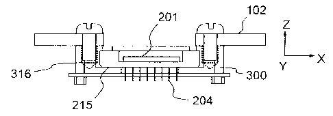
module according to the invention is described in relation to Figures 4 and 5.
It comprises a cradle in the form of a rigid frame 300 in which the sensor 200
is positioned and glued by its rear face 215. The aperture 314 of the frame is
provided to allow the passage of the electrical connections 204. It is
generally
rectangular but not necessarily.
This frame 300 is machined from a block with two planes which
are:
- the mounting plane 301 for gluing the sensor and
- the plane of the top face 302.
One of these two planes is a reference plane. Hereinafter in the
description, it is considered that it is the plane of the top face 302.
The frame 300 comprises:
- in the mounting plane 301, bearing points 313 for the sensor
(preferably three bearing points) used to align the chip 201 in relation
to the reference plane of the frame, in the three axes,
- on its top face 302, reference points 317 for fixing the camera
objective 102 intended to centre and align the optical axis of the
camera objective in relation to the reference plane of the frame. In our
example, two reference points are used, one oblong and the other
CA 2989486 2017-12-19
6
round; it is of course possible to use one or more other reference
points,
- on its
top face 302, tappings 316 or other equivalent means
intended to cooperate with means for fixing the camera objective 102
on the frame.
The outline of the frame is parallelepipedal, possibly dished on the
outside as in the example of Figure 5 with two dished sides. The internal
outline of the frame has a form corresponding to that of the sensor.
The step of gluing the sensor 200 in the frame 300 is performed by
a positioning machine of "pick and place" type for example. The machine
deposits a glue on the gluing surface 301 of the frame (= bearing surface of
the sensor), then positions the sensor 200 in the frame on this surface, then
performs the optical alignment of the chip 201 in relation to the frame (that
is
to say in relation to the reference planes) by adjusting the position of the
sensor in the three axes by virtue of the bearing points 313. This alignment
makes it possible to correct the error of perpendicularity of the chip 201 in
relation to the reference plane, as well as the offset in the mounting plane,
that is to say the errors illustrated in Figures 3a and 3b. The machine holds
the assembly (sensor + frame) in position during the polymerization of the
glue. The glue is typically an epoxy resin with or without fillers. This step
is
performed in a single stage and dispenses with all the subsequent setting
operations. After the gluing of the sensor, the sensitive face of the chip 201
(= face opposite the connection pins) is therefore collinear to the reference
plane, in this case to the top surface 302 of the frame.
A positioning accuracy in the mounting plane is thus obtained that
is typically of the order of 35 pm.
With the sensor being thus fixed to the frame, the camera
objective 102 of an image-forming device will be able to be fixed to the frame
300 by virtue of the fixing reference points 317 and of the tappings 316 on
the top face of the frame as can be seen in Figures 4 and 5. On completion
of these two steps (gluing the sensor and fixing the camera objective), there
will be an assurance that:
CA 2989486 2017-12-19
7
.
- the photosensitive face of the chip is collinear to the reference
plane of the frame and centred, and that
-
the optical axis of the camera objective is at right angles to the
reference plane of the frame and that the camera objective is centred.
The same steps are applied considering the mounting plane 301
as reference plane
The mounting plane and that of the top face are advantageously
collinear by construction.
The chip 201 can comprise 4 million pixels.
The frame is advantageously made of a thermally conductive
material such as aluminium or copper. Before the gluing step, a thermal
interface 318 shown in Figure 6 is preferably placed on the gluing surface
301. This thermal interface allows the passage of the electrical connection
pins 204 while ensuring a good thermal contact on the periphery of the
sensor. This thermal interface makes it possible to ensure the exchanger and
radiator functions in one and the same product. A thermally conductive glue
is typically used, such as a UV glue which also makes it possible to fix the
sensor 200 in the frame as indicated previously. By using an epoxy resin with
or without fillers as glue, the thermal conductivity obtained is less than 4
C/W
between the sensor 200 and the mechanical fixing plane 301.
When the sensor has been fixed to the frame, the sensor + frame
assembly is assembled with a stack of printed circuit boards 400 each
comprising one or more active and/or passive electronic components 401 on
one face or on both its faces, as shown in Figures 7a, 7b with a stack of four
printed circuit boards 400. These components 401 are typically passive
components for filtering parasitic interferences, for protecting the sensor,
and
active components such as processing units for the signals received by the
chip, power supplies.
One of the problems with the sensors is jointly ensuring the
mechanical fixing and the electrical link with these printed circuit boards.
The
connection to these printed circuit boards is made through a first printed
circuit board PCB which comprises electrical connection contacts, and
possibly electronic components. This PCB 400 is fixed to the frame 300 and
CA 2989486 2017-12-19
8
the connection pins 204 of the sensor 200 are electrically linked to the
connection contacts of the PCB by brazing. For example, the pins 204 pass
through the PCB and are brazed on the bottom face side of the PCB. The
frame 300 is thus sandwiched between the sensor and the PCB. This aspect
reinforces the mechanical strength and the PCB does not need to be
specifically in the same plane as the sensor 200 or the chip 201. This layout
makes it possible to have a proximity between the chip and the electronic
components of the stack, even by using a thermal interface as indicated
previously. This solution makes it possible to significantly reduce the
electronic noises which come into play in image capture.
As can be seen in Figure 7a, the sensor + cradle + stack assembly
is then moulded in resin 500 up to the reference plane 302 of the cradle or
slightly below as can be seen in the figure; the dimensions according to XY of
the frame are less than those of the stack as can be seen in the figure. The
moulded assembly is then cut according to the vertical cutting axes 501 (in
the axis Z) with which electrically conductive tracks 402 of each printed
circuit
board are flush as shown in Figure 7b. The vertical faces are then metallized
and etched to produce the electrical interconnections 502 between the
circuits of the stack as shown in Figure 8. The last printed circuit board 400
is
provided with external electrical connection means 404.
Such a module of which an example is shown in Figure 8 with:
- interconnection tracks 502 on its side faces,
- the cradle 300 of which can be seen the top face with its tappings
316 and its reference points 317 for fixing an image-forming device
100,
- the sensor of which the protective glass 202 and the package 203
can be seen,
will then be able to be associated with an image-forming device 100 with a
view to an imaging application, in particular a space imaging application.
CA 2989486 2017-12-19