Note : Les descriptions sont présentées dans la langue officielle dans laquelle elles ont été soumises.
CA 02990357 2017-12-20
DESCRIPTION
HIGH-FREQUENCY LINE
Technical Field
[0001] The present invention relates to a high-frequency
line to apply an electric signal to a modulation electrode of
an optical modulator or the like.
Background Art
[0002] There has been a demand for capacity enlargement of
an optical communication system along with an explosive
increase in data communication traffic in recent years, and
developments in integration and complication of optical
components used therein as well as an increase in speed of
signals are in progress. Examples of such optical components
include optical modulators. A polarization multiplexing
optical I/Q modulator in which two optical I/Q modulators (see
Non Patent Literature 1, for example), each based on a
Mach-Zehnder (MZ) modulator adaptable to multilevel modulation
such as QPSK (quadrature phase shift keying) and 16QAM (16
quadrature amplitude modulation), are integrated for two
polarized optical waves (a configuration including four
Mach-Zehnder modulators integrated in total) has been
increasingly used nowadays in order to enlarge a transmission
capacity.
- 1 -
CA 02990357 2017-12-20
[0003] This polarization multiplexing optical I/4
modulator can generate an optical modulation signal in the order
of 100 Gbits/s. However, in this process, it is necessary to
input a high-speed electric signal at a symbol rate of several
tens of gigahertz to each Mach-Zehnder modulator in the chip.
Usually, a high-frequency signal inputted through an RF
interface of a polarization multiplexing optical I/Q modulator
module package is passed through a high-frequency wiring board
in the module package and eventually supplied to the
polarization multiplexing optical I/Q modulator chip. In
order to suppress power loss and crosstalk in the above process,
it is essential to minimize wiring for connection between the
high-frequency wiring board and the polarization multiplexing
optical I/Q modulator chip.
[0004] To this end, the RF interface of the polarization
multiplexing optical I/Q modulator chip needs to be located at
an end of the chip by appropriately laying out a high-frequency
wiring in the chip. Fig. 1 shows a configuration of a
polarization multiplexing optical I /Q modulator in which 50-ohm
microstrip lines formed on a SI-InP substrate intersect with
InP-based optical waveguides. As a consequence, each
high-frequency line 103 connected to a modulation electrode 102
inevitably intersects with the optical waveguides 101 that
propagate optical signals.
Citation List
Non Patent Literature
- 2 -
CA 02990357 2017-12-20
[0005] NPL 1: Nobuhiro Kikuchi, et al., "80-Gb/s
Low-Driving-Voltage InP DQPSK Modulator With an n-p-i-n
Structure", IEEE PHOTONICS TECHNOLOGY LETTERS, Vol.21, No.12,
JUNE 15, 2009.
Summary of Invention
(Technical Problem)
[0006] Now, effects of intersection of high-frequency
wiring and optical waveguides on power loss and characteristic
impedance will be described based on a result of simulating a
situation where the high-frequency wiring intersects with the
optical waveguides. Figs. 2A and 2B illustrate models of a
microstrip line not having intersection with optical waveguides
and of a microstrip line having intersection with optical
waveguides which are used in the simulation, respectively. In
the simulation, a length of each line is set to 1.4mm. Moreover,
on the assumption that the polarization multiplexing optical
I/Q modulator is formed from four Mach-Zehnder modulators, the
line intersects with the optical waveguides 7 times at the
maximum, and calculation is conducted by assigning 7 as the
number of times of intersection. As for the simulation method,
the 1.4-mm line is equally divided into seven 200- m segments,
each of which is then subjected to calculation in the case of
not having the intersection with the optical waveguides and the
case of having the intersection with the optical waveguides,
and a result on the entire 1.4-mm line is calculated by
multiplying the obtained results (a matrix).
- 3 -
I
CA 02990357 2017-12-20
[0007] Figs. 3A and 3B show simulation results of power loss
(S21 characteristic, 50-ohm) and characteristic impedance,
respectively, in the presence and absence of the intersection
of the microstrip line with the optical waveguides. The results
show that the high-frequency wiring having the intersection
with the optical waveguides exhibits an increase in insertion
loss (S21) and a rise in characteristic impedance as compared
to the high-frequency wiring not having the intersection.
[0008] As described above, the conventional high-frequency
wiring in the polarization multiplexing optical I/Q modulator
or the like has a problem of significant deterioration in the
characteristics of the high-frequency line due to the
intersection with the optical waveguides.
[0009] The present invention has been made in view of the
aforementioned problem, and an object thereof is to provide a
high-frequency line including a structure to suppress an
impedance variation and occurrence of an excessive power loss
in high-frequency wiring having intersection with an optical
waveguide.
[0010] To solve the problem, the present invention provides
a high-frequency line including a dielectric body, a signal
electrode, and a ground electrode and configured to transmit
a high-frequency electric signal, which is characterized in
that when the high-frequency line is divided into segments each
having a length shorter than a wavelength of the high-frequency
electric signal, the signal electrode, the ground electrode,
and the dielectric body in one of the segments having
- 4 -
CA 02990357 2017-12-20
intersection of the high-frequency line with an optical
waveguide are structured to have characteristic impedance equal
to the characteristic impedance in another one of the segments
not having the intersection of the high-frequency line with the
optical waveguide.
[0011] Another aspect of the present invention is
characterized in that the signal electrode in the segment having
the intersection of the high-frequency line with the optical
waveguide has two or more different widths.
[0012] Another aspect of the present invention is
characterized in that the signal electrode in the segment having
the intersection of the high-frequency line with the optical
waveguide has two or more different thicknesses.
[0013] Another aspect of the present invention is
characterized in that a gap between the signal electrode and
the ground electrode in the segment having the intersection of
the high-frequency line with the optical waveguide has two or
more different distances.
[0014] Another aspect of the present invention is
characterized in that the dielectric body in the segment having
the intersection of the high-frequency line with the optical
waveguide has two or more different dielectric constants.
[0015] Another aspect of the present invention is
characterized in that the dielectric body in the segment having
the intersection of the high-frequency line with the optical
waveguide has two or more different thicknesses.
- 5 -
[0016] Another aspect of the present invention is characterized
in that the high-frequency line is a microstrip line.
[0017] Another aspect of the present invention is characterized
in that the high-frequency line is a coplanar line.
[0018] Another aspect of the present invention is characterized
in that the high-frequency line is a grounded coplanar line.
Advantageous Effects of Invention
[0019] According to the present invention, it is possible to
suppress an impedance variation and occurrence of an excessive
power loss in high-frequency wiring having intersection with an
optical waveguide.
[0019a] In an aspect, there is provided a high-frequency line
formed on a substrate comprising an optical waveguide, including
a dielectric body, a signal electrode, and a ground electrode and
configured to transmit a high-frequency electric signal in a
propagation direction, said signal electrode extending in the
propagation direction of the high frequency electric signal,
characterized in that the high-frequency line comprises segments
each having a length shorter than a wavelength of the high-frequency
electric signal; in one of the segments the optical waveguide
crosses the signal electrode in spaced relation to the signal
electrode; the signal electrode, the ground electrode, and the
dielectric body in said one of the segments where the optical
waveguide crosses the signal electrode are configured to have a
characteristic impedance equal to the characteristic impedance in
another one of the segments where the signal electrode and the
optical waveguide do not cross.
- 6 -
CA 2990357 2019-08-29
Brief Description of Drawings
[0020]
[Fig. l] Fig. 1
is a diagram showing a configuration of a
polarization multiplexing optical I/Q modulator including
microstrip lines;
[Fig. 2A] Fig. 2A is a diagram showing a model of a microstrip
line not having intersection with optical waveguides, which is used
in a simulation;
[Fig. 2B] Fig. 2B is a diagram showing a model of a microstrip
line having intersection with optical waveguides, which is used
in the simulation;
- 6a -
CA 2990357 2019-08-29
CA 02990357 2017-12-20
[Fig. 3A] Fig. 3A is a diagram showing a simulation result of
power loss (S21 characteristic, 50-ohm) in terms of the presence
and absence of the intersection of the microstrip line with the
optical waveguides, respectively;
[Fig. 30] Fig. 30 is a diagram showing a simulation result of
characteristic impedance in terms of the presence and absence
of the intersection of the microstrip line with the optical
waveguides, respectively;
[Fig. 4A] Fig. 4A is a top plan view of a high-frequency line
according to a first embodiment of the present invention;
[Fig. 40] Fig. 4B is a cross-sectional view of the
high-frequency line according to the first embodiment of the
present invention, which is taken along the IVB-IVB line in FIG.
4A;
[Fig. 4C] Fig. 4C is a transverse sectional view of the
high-frequency line according to the first embodiment of the
present invention, which is taken along the IVC-IVC line in FIG.
4A;
[Fig. 40] Fig. 40 is a transverse sectional view of the
high-frequency line according to the first embodiment of the
present invention, which is taken along the line in FIG.
4A;
[Fig. 5A] Fig. 5A is a diagram showing a model of a microstrip
line not having intersection with optical waveguides, which is
used in a simulation;
- 7 -
CA 02990357 2017-12-20
=
[Fig. 5B] Fig. 5B is a diagram showing a model of a microstrip
line having intersection with optical waveguides, which is used
in the simulation;
[Fig. 5C] Fig. 5C is a diagram showing a model of a microstrip
line having intersection with optical waveguides and including
a compensation structure using second signal electrode portions
325, which is used in the simulation;
[Fig. 6A] Fig. 6A is a diagram showing simulation results of
power loss (S21 characteristic, 50-ohm) in the case of not
having the intersection of the microstrip line with the optical
waveguides, in the case of having the intersection of the
microstrip line with the optical waveguides, and in the case
of having the intersection with the optical waveguides and
including the compensation structure using the second signal
electrode portions 325;
[Fig. 6B] Fig. 6B is a diagram showing simulation results of
characteristic impedance in the case of not having the
intersection of the microstrip line with the optical waveguides,
in the case of having the intersection of the microstrip line
with the optical waveguides, and in the case of having the
intersection with the optical waveguides and including the
compensation structure using the second signal electrode
portions 325;
[Fig. 7A1 Fig. 7A is a top plan view of a high-frequency line
according to a second embodiment of the present invention;
[Fig. 713} Fig. 7B is a cross-sectional view of the
high-frequency line according to the second embodiment of the
- 8 -
CA 02990357 2017-12-20
=
present invention, which is taken along the VIIB-VIIB line in
FIG. 7A;
[Fig. 7C] Fig. 7C is a transverse sectional view of the
high-frequency line according to the second embodiment of the
present invention, which is taken along the VIIC-VIIC line in
FIG. 7A;
[Fig. 7D] Fig. 7D is a transverse sectional view of the
high-frequency line according to the second embodiment of the
present invention, which is taken along the VIID-VIID line in
FIG. 7A;
[Fig. 8A] Fig. 8A is a diagram showing an example of simulating
a difference in characteristic concerning the power loss (the
S21 characteristic) of a grounded coplanar line designed for
50 n and depending on the presence and absence of the
intersection with the optical waveguides;
[Fig. 8B] Fig. 831s a diagram showing an example of simulating
a difference in characteristic concerning the characteristic
impedance of the grounded coplanar line designed for 50 Q and
depending on the presence and absence of the intersection with
the optical waveguides;
[Fig. 9A] Fig. 9A is a top plan view of a different grounded
coplanar line according to a third embodiment of the present
invention;
[Fig. 9B] Fig. 9B is a cross-sectional view of the different
grounded coplanar line according to the third embodiment of the
present invention, which is taken along the IXB-IXB line in Fig.
9A;
- 9 -
CA 02990357 2017-12-20
[Fig. 9C] Fig. 9C is a transverse sectional view of the
different grounded coplanar line according to the third
embodiment of the present invention, which is taken along the
IXC-IXC line in Fig. 9A;
[Fig. 9D] Fig. 9D is a transverse sectional view of the
different grounded coplanar line according to the third
embodiment of the present invention, which is taken along the
IXD-IXD line in Fig. 9A;
[Fig. 10A] Fig. 10A is a top plan view of an eclectic structure
of a different microstrip line and a grounded coplanar line
according to a fourth embodiment of the present invention;
[Fig. 10B] Fig. 10B is a cross-sectional view of the eclectic
structure of the different microstrip line and the grounded
coplanar line according to the fourth embodiment of the present
invention, which is taken along the XB-XB line in Fig. 10A;
[Fig. 10C] Fig. 10C is a cross-sectional view of the eclectic
structure of the different microstrip line and the grounded
coplanar line according to the fourth embodiment of the present
invention, which is taken along the XC-XC line in Fig. 10A;
[Fig. 10D] Fig. 10D is a transverse sectional view of the
eclectic structure of the different microstrip line and the
grounded coplanar line according to the fourth embodiment of
the present invention, which is taken along the XD-XD line in
Fig. 10A; and
[Fig. 10E] Fig. 10E is a transverse sectional view of the
eclectic structure of the different microstrip line and the
grounded coplanar line according to the fourth embodiment of
- 10 -
CA 02990357 2017-12-20
the present invention, which is taken along the XE-XE line in Fig.
10A.
Description of Embodiments
[0021] Embodiments of the present invention will be described
below in detail.
(First Embodiment)
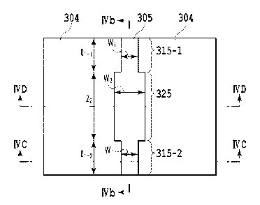
[0022] Fig. 4A shows a top plan view of a segment unit of a
high-frequency line according to a first embodiment of the present
invention, Fig. 4B shows a cross-sectional view thereof taken along
the IVB-IVB line, Fig. 4C shows a transverse sectional view thereof
taken along the IVC-IVC line, and Fig. 4D shows a transverse sectional
view thereof taken along the IVD-IVD line, respectively. The
high-frequency line of this embodiment is a microstrip line and has
a basic configuration in which a ground electrode 302, a dielectric
layer 304, and a signal electrode 305 are sequentially stacked on
a SI-InP substrate 301. In addition, as shown in the transverse
sectional view, an optical waveguide core 303 made of InP-based
semiconductor intersects with the high-frequency line in a crossing
manner.
[0023] The presence of the intersection with the optical
waveguide causes partial disconnection of the ground electrode 302
of the high-frequency line along a propagating direction, and part
of the dielectric layer 304 is replaced with an InP-based material
as shown in the cross-sectional view of Fig. 4B and the transverse
sectional view of Fig. 4D. As a
- 11 -
CA 02990357 2017-12-20
4
consequence, a dielectric constant between the ground electrode
302 and the signal electrode 305 is partially changed. This
means that characteristic impedance of the high-frequency line
varies in a region of intersection with the optical waveguide,
and an excessive loss of power is induced in the case of a
conventional structure in which the signal electrode is uniform
in the propagating direction.
[0024] As mentioned above, in the case of having the
intersection with the optical waveguides while not including
a compensation structure (in a uniform structure in the
propagating direction) , the S21 characteristic is deteriorated
(the power loss is increased) and the characteristic impedance
rises significantly as compared to the case of not having the
intersection with the optical waveguides. Deviation of the
characteristic impedance from a designed value causes
reflection of an electric signal whereby the characteristic is
deteriorated.
[0025] Accordingly, in this embodiment, the width of the
signal electrode 305 is partially increased in a certain region
covering the intersection with the optical waveguides along the
propagating direction of the high-frequency line, and based on
each segment obtained by equally dividing the high-frequency
line as shown in Figs. 4A to 4D. In the microstrip line, an
increase in width of the signal electrode 305 partially from
INT_ to w2 brings about an effect to reduce the characteristic
impedance as compared to the one with the uniform width wi-
- 12 -
CA 02990357 2017-12-20
[0026] The length (11-1+12+11-2) of each segment is set to
a sufficiently shorter length (about 1/10 or below in general)
than a wavelength of a high-frequency electric signal to be
inputted. Thus, the entire characteristic impedance including
front and back portions of the high-frequency line can be
regarded as the characteristic impedance obtained by adding up
respective characteristic impedances according to the ratios
of a length of a second signal electrode portion 325 having the
width w2 to a length of a first signal electrode portions 315
located at the front and back thereof and having the width 141,
and then averaging the added value. Accordingly, the electrode
width w2 of the second signal electrode portion 325 may be set
depending on the desired characteristic impedance and an
allowable length 12 of the second signal electrode portion 325.
[0027] Figs. aA to SC show models of the microstrip line
not having the intersection with the optical waveguides, the
microstrip line having the intersection with the optical
waveguides, and the microstrip line having the intersection
with the optical waveguides and including a compensation
structure using the second signal electrode portions 325,
respectively, which are used in the simulation. In the meantime,
Figs. 6A and 6B show simulation results concerning power loss
(S21 characteristic, 50-ohm) and characteristic impedance in
the case of not having the intersection of the microstrip line
with the optical waveguides, in the case of having the
intersection of the microstrip line with the optical waveguides,
and in the case of having the intersection with the optical
- 13 -
CA 02990357 2017-12-20
waveguides and including the compensation structure using the
second signal electrode portions 325. Effects of suppressing
a rise in power loss (S21) and a rise in characteristic impedance
due to the intersection with the optical waveguides, the effects
being attributed to the presence of the compensation structure
using the second signal electrode portions 325, can be confirmed
from Figs. 6A and 6B.
[0028] This embodiment shows an example of increasing the
width w2 of each second signal electrode portion 325 of the
signal electrode 305 of the microstrip line, the second signal
electrode portion 325 covering the region intersecting with the
optical waveguide. Nonetheless, what is required here is to
obtain the desired characteristic impedance on average in a
certain region such as a segment of 200 i.tm. In this context,
the width w1 of the signal electrodes of the first signal
electrode portions 315 at the front and back of the region
intersecting with the optical waveguide may be set larger than
the width w2 of the second signal electrode portion 325 instead.
(Second Embodiment)
[0029] Fig. 7A shows a top plan view of a segment unit of
a high-frequency line according to a second embodiment of the
present invention, Fig. 7B shows a cross-sectional view thereof
taken along the VIIB-VIIB line, Fig. 70 shows a transverse
sectional view thereof taken along the VIIC-VIIC line, and Fig.
7D shows a transverse sectional view thereof taken along the
VIID-VIID line, respectively. The high-frequency line of this
embodiment is a grounded coplanar line and has a basic
- 14 -
CA 02990357 2017-12-20
configuration in which a lower-layer ground electrode 702, a
dielectric layer 704, a signal electrode 705, and an upper-layer
ground electrode 706 are sequentially stacked on a SI-InP
substrate 701. In addition, as shown in the transverse
sectional view, an optical waveguide core 703 made of InP-based
semiconductor intersects with the high-frequency line in a
crossing manner.
[0030] The presence of the intersection with the optical
waveguide causes a partial change in dielectric constant
between the lower-layer ground electrode 702 and the signal
electrode 705 as described in the first embodiment. This means
that the characteristic impedance of the high-frequency line
varies in the region of intersection with the optical waveguide,
and an excessive loss of power is induced in the case of the
conventional structure in which the signal electrode is uniform
in the propagating direction.
[0031] Figs. 8A and 8B show an example of simulating
differences in characteristic concerning the power loss (the
S21 characteristic) and the characteristic impedance of a
grounded coplanar line designed for 50 11 and depending on the
presence and absence of the intersection with the optical
waveguides. In the calculation, as with the first embodiment,
the calculation is conducted by setting the length of the line
to 1.4 mm and setting the number of times of intersection to
seven times in the case of having the intersection.
[0032] As shown in Figs. 8A and 8B, in the case of having
the intersection with the optical waveguides while not
- 15 -
CA 02990357 2017-12-20
=
=
including a compensation structure, it is confirmed that the
S21 characteristic is deteriorated (the power loss is
increased) and the characteristic impedance rises as compared
to the case of not having the intersection with the optical
waveguides.
[0033] Accordingly, in this embodiment, the width of the
signal electrode 705 is partially increased in a certain region
covering the intersection with the optical waveguides along the
propagating direction of the high-frequency line, and based on
each segment obtained by equally dividing the high-frequency
line as shown in Figs. 7A to 7D. In the grounded coplanar line,
an increase in width of the signal electrode 705 partially from
wl to w2 brings about an effect to reduce the characteristic
impedance as compared to the one with the uniform width wi =
[0034] The length (11_1+12+11_2) of the segment is set to a
sufficiently shorter length than a wavelength of a
high-frequency electric signal to be inputted (about 1/10 or
below in general) . Thus, the entire characteristic impedance
including front and back portions of the high-frequency line
can be regarded as the characteristic impedance obtained by
adding up respective characteristic impedances according to the
ratios of a length of a second signal electrode portion 725
having the width w2 to a length of a first signal electrode
portions 715 located at the front and back thereof and having
the width w1, and then averaging the added value. Accordingly,
the electrode width w2 of the second signal electrode portion
725 may be set depending on the desired characteristic impedance
- 16 -
CA 02990357 2017-12-20
and an allowable length 12 of the second signal electrode portion
725.
[0035] In the case with the compensation structure (a
large-width signal electrode) using the second signal electrode
portion 725 having the width w2, an effect to suppress a rise
in characteristic impedance is confirmed in particular as shown
in Fig. 8B.
[0036] This embodiment shows an example of increasing the
width w2 of each second signal electrode portion 725 of the
signal electrode 705 of the grounded coplanar line, the second
signal electrode portion 725 covering the region intersecting
with the optical waveguide. Nonetheless, what is required here
is to obtain the desired characteristic impedance on average
in a certain region such as a segment of 2001AM. In this context,
the width w1 of the signal electrodes of the signal electrode
portions 715 at the front and back of the region intersecting
with the optical waveguide may be set larger than the width la')
of the second signal electrode portion 725 instead.
(Third Embodiment)
[0037] Furthermore, Fig. 9A shows a top plan view of a
grounded coplanar line according to a third embodiment of the
present invention, Fig. 9B shows a cross-sectional view thereof
taken along the IXB-IXB line, Fig. 9C shows a transverse
sectional view thereof taken along the IXC-IXC line, and Fig.
9D shows a transverse sectional view thereof taken along the
IXD-IXD line, respectively. A signal electrode width 905 may
be set uniform, and meanwhile, a width of each upper-layer
- 17 -
CA 02990357 2017-12-20
ground electrode 906 maybe increased in a region intersecting
with an optical waveguide, and a gap between the signal
electrode 905 and each upper-layer ground electrode 906 may be
changed, or more specifically, narrowed as shown in Fig. 9A.
In this case of having the compensation structure (a narrow SG
gap electrode), an effect to suppress a rise in characteristic
impedance and an effect to suppress an increase in excessive
power loss are confirmed as shown in Fig. BE.
(Fourth Embodiment)
[0038] Fig. 10A shows a
top plan view of an eclectic
structure of a microstrip line and a grounded coplanar line
according to a fourth embodiment of the present invention, Fig.
10B shows a cross-sectional view thereof taken along the XB-XB
line, Fig. 10C shows a cross-sectional view thereof taken along
the XC-XC line, Fig. 10D shows a transverse sectional view
thereof taken along the XD-XD line, and Fig. 10E shows a
transverse sectional view thereof taken along the XE-XE line,
respectively. This structure provides a ground electrode 1002
in a region intersecting with the optical waveguide as shown
in Fig. 10E, which is located at the same position as any of
the upper-layer ground electrodes 706 and 906 of the grounded
coplanar lines, and provides the ground electrode 1002 only on
a SI-InP substrate 1001 like a microstrip line as shown in Fig.
101) at portions at the front and back of the region intersecting
with the optical waveguide. Regarding the high-frequency line
shown in Figs. 10A to 10E as well, it is possible to suppress
a rise in characteristic impedance and an increase in excessive
- 18 -
CA 02990357 2017-12-20
power loss by providing a signal electrode 1005 with the compensation
structure as with the first and second embodiments.
[0039] Note that the first to fourth embodiments show the examples
of providing any of the signal electrode and the ground electrode
with the compensation structure. Instead, other compensation
structures may be used while changing a thickness of any of the
electrodes, a gap between the signal electrode and the ground
electrode, a dielectric constant and/or a thickness of the dielectric
layer, which represent parameters that can change the characteristic
impedance.
[0040] In the meantime, while the first to fourth embodiment show
the examples of the high-frequency lines each of which consists of
either the structure of the microstrip line, the structure of the
grounded coplanar line or the eclectic structure of them, the basic
structure of the high-frequency line may of course be changed in the
middle. In addition, while the signal electrode and the ground
electrode are formed to be attached onto the dielectric body, those
electrodes may partially be formed into air-bridge structure.
[0041] As described above, it is possible to suppress a variation
in impedance or occurrence of an excessive power loss by partially
changing the structure of the high-frequency line depending on the
intersection with the optical waveguide.
Reference Signs List
[0042]
- 19 -
CA 02990357 2017-12-20
101 optical waveguide
102 modulation electrode
103 high-frequency line
301, 701, 901, 1001 SI-InP substrate
302, 702, 706, 902, 1002 ground electrode
303, 703, 903, 1003 optical waveguide core
304, 704, 904, 1004 dielectric layer
305, 705, 905, 1005 signal electrode
- 20 -