Note : Les descriptions sont présentées dans la langue officielle dans laquelle elles ont été soumises.
1
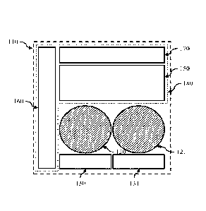
SPAD ARRAY STRUCTURES AND METHODS OF OPERATION
PRIORITY DOCUMENTS
[0001] The present application claims priority from Australian Provisional
Patent Application No.
2015902699 titled "SPAD ARRAY STRUCTURES AND METHODS OF OPERATION" and filed
on
08 July 2015.
TECHNICAL FIELD
[0002] The present disclosure relates to sensor circuits comprising an array
of Single-Photon Avalanche
Diode (SPAD) circuits.
BACKGROUND
[0003] Avalanche photodiodes (APDs) are solid-state photodetectors in which a
high bias voltage is
applied to a p-n junction to provide a high first stage gain due to avalanche
multiplication. Avalanche
multiplication occurs when an incident photon with sufficient energy to
liberate an electron arrives at the
photodiode. The high electric field rapidly accelerates the photo-generated
electron towards the anode,
but before it can reach the anode, it collides with the intervening doped
material releasing further
electrons, all of which are then accelerated towards the anode. This process
repeats leading to avalanche
multiplication of the photo-generated electron and an output current pulse.
APDs are thus semiconductor
analogs to photomultiplier tubes. Linear mode APDs are effectively single
stage linear amplifiers in
which the gain is set by controlling the bias voltage, and with gain factors
of several hundred can be
achieved in linear mode.
[0004] Single-Photon Avalanche Diodes (SPADs) are APDs in which the p-n
junction is biased above its
breakdown voltage to operate in Geiger mode such that a single incident photon
will trigger an ongoing
avalanche breakdown and thus easily measureable current pulse. That is a SPAD
operates as a trigger
device generating a large current pulse compared to linear mode APDs in which
the current pulses can be
very low at low light intensity. After triggering of the SPAD, a quenching
circuit is used to reduce the
bias voltage below the breakdown voltage in order to quench the avalanche
process. Once quenched the
bias voltage is again raised above the breakdown voltage to reset the SPAD for
detection of another
photon (known as re-biasing the SPAD).
[0005] APD and SPADs are solid state devices and can be constructed using a
variety of CMOS
technologies, and have very small active areas compared with other photon
counting devices such as
photomultiplier tubes. Through appropriate choice of materials and structure,
wavelength sensitivity of a
Date Recue/Date Received 2022-11-07
2
SPAD can be controlled to be in the visible and/or near-infrared range. A SPAD
combined with
additional circuitry to count pulses and/or measure time of arrival of photons
to sub-nano/pico second
accuracy can be used to create sensors for ultra-low light imaging or highly
sensitive time-resolved
imaging applications. For example one potential application of a SPAD arrays
are in three dimensional
(3D) Flash LIDAR cameras, as they have the potential to provide extremely
sensitive devices with high
distance resolution and high frame rates. SPAD arrays also have potential for
use in other applications
that require single photo sensitivity with high frames such as
biological/medical imaging applications,
adaptive optics applications, and astrophysics applications.
[0006] Three dimensional Flash LIDAR systems, also known as 3D Time of Flight
(TOF) Cameras, use
a laser source to irradiate a target with a short duration laser pulse (ie a
laser flash). Photons are back
scattered off objects and onto the sensor and the time of arrival is used to
determine time of flight and
thus distance to an object. The first 3D TOF cameras were constructed as
scanning laser systems
comprising a laser range finder with a rotating or scanning element(s) to
progressively scan the field of
view. These scanning systems are effectively single pixel devices collecting
time of flight information in
a single direction which build up a 3D image progressively moving the pointing
direction of the sensing
element. More recently scanner-less (ie staring) 3D Flash LIDAR systems have
been developed using a
two dimensional array of linear mode APDs (pixels) to achieve more rapid scene
capture than scanning
systems, and to avoid problems with scanning systems such as mechanical wear,
vibration, and/or motion
blur. By rapidly resetting APDs after triggering, each pixel can be used to
receive multiple photons from
the laser pulse, each corresponding to different distance. In this way, a 3D
point cloud of the target scene
can be rapidly generated.
[0007] SPAD arrays in 3D Flash LIDAR systems have the potential to achieve
even greater light
sensitivity with high distance resolution and high frame rates than scanning
laser systems or scanner-less
APD based systems. However, achieving high spatial resolution with a SPAD
array has proved
challenging and most SPAD arrays are experimental with only a relatively small
number of pixels (eg
6x8, 32x32). In particular SPADs require the use of very high voltages, and
design of efficient SPAD
structure is a difficult problem. Further each SPAD requires an adjacent
quenching circuit and a
triggering detection (ie time of arrival) circuit, all of which takes up
additional space on the substrate
immediately surrounding the SPAD.
[0008] There is thus a need to provide improvements to allow construction of
high density SPAD arrays,
or at least provide a useful alternative to current SPAD array systems.
Date Recue/Date Received 2022-11-07
3
SUMMARY
[0009] According to a first aspect, there is provided a Single-Photon
Avalanche Diode (SPAD) array
comprising a plurality of SPAD cells, each SPAD cell comprising:
a plurality (n) of SPAD structures;
a plurality (n) quenching circuits, each quenching circuit connected to one of
the SPAD
structures;
a common trigger circuit connected to each of the SPAD structures and further
comprising:
a counter configured to enable determination of a triggering time of one or
more of the
plurality of SPAD structures with respect to a start signal;
a memory,
a plurality (n) of latches each connected to a SPAD structure and a logic
circuit
connected to the plurality of latches and configured to stop the counter if
all of the latches are
triggered;
a pulse latch and write circuit with a plurality (n) of inputs, each input
connected to a
SPAD structure and configured to detect an output pulse from a SPAD structure,
and each time
an output pulse is detected the SPAD ID of the SPAD structure the output pulse
was detected
from is provided to the memory and the value of the counter is read and stored
in memory with
the SPAD ID.
[0010] In one form, the counter is at least a 16 bit counter.
[0011] In one form, the memory is configured to store n -J values and each
value has bit size of at least
the bit size of the counter, plus the number of bits required to represent n -
/.
[0012] In one form, n =2.
[0013] In one form, the array is at least a 128x128 cell array.
[0014] In one form, each SPAD structure comprises a Pwell region comprising at
least one anode and an
active region on a top surface, a Pdrift region, and an Nwell region
comprising at least one cathode and
surrounding the Pwell region, wherein the Pdrift region is a lightly doped
guard ring surrounding the
Pwell region and partially extending beneath the Pwell region such that when
viewed from above the
Pdrift region overlaps with the Pwell region, and the Pdrift region separates
the Pwell region from the
surrounding Nwell region apart from a junction region formed at an interface
of the lower surface of the
Pwell region and the Nwell region.
Date Recue/Date Received 2022-11-07
4
[0015] In further form, in each SPAD structure the Pwell region is a circular
disk region extending from
a top surface of the SPAD into the Nwell region, the Pdrift region is an
annular region with a thickness
greater than the thickness of the Pwell region and extending radially from the
Pwell region, and extending
beneath the Pwell region into the Nwell region to define an overlapping
region.
[0016] In a further form, in each SPAD structure the ratio of a width of the
overlapping region to the
diameter of the active region is in the range 0.05 to 0.25.
[0017] In one form, each SPAD structure comprises a Pwell region comprising at
least one anode, an
active region on a top surface of the Pwell region, a Pdrift region in an
implantation region, and a Nwell
region comprising at least one cathode and a junction region formed at an
interface of the lower surface of
the Pwell region and the Nwell region, wherein a top surface of the active
region of the SPAD is exposed
and a top surface of the Nwell region is covered with one or more shallow
trench isolation (STI) regions,
and a polysilicon gate (Poly) region is placed over a top surface of the
implantation region apart from the
exposed active region and extends over a portion of the top surface of the
Nwell region to separate one or
more STI regions from the implantation region.
[0018] In a further form, each SPAD structure the polysilicon gate is kept at
the same potential as the
Pwell region.
[0019] According to a second aspect, there is provided a method for recording
triggering times of a
plurality of SPAD structures, the method comprising:
starting a counter in a cell wherein the counter is configured to enable
determination of a
triggering time of one or more of the plurality of SPAD structures with
respect to a start signal;
detecting each output pulse from one of the plurality of SPAD structures in
the cell;
for the first n -1 detected output pulses capturing the value of the counter
and storing the counter
value in a memory with a SPAD ID of the SPAD structure the output pulse was
detected from; and
for the nth the detected output pulse either stopping the counter or capturing
the value of the
counter and storing the counter value in the memory of a common trigger
circuit connected to each of the
SPAD structures with a SPAD ID of the SPAD structure the output pulse was
detected from; and
reading each stored counter value and associated SPAD ID from the memory and
reading the
current counter value if it was stopped by the nth the detected output pulse
[0020] In one form, for the nth the detected output pulse the counter is
stopped.
[0021] In one form, after each detected output pulse from one of the plurality
of SPAD structures the
SPAD that generated the output pulse is re-biased and for the nth and each
subsequent detected output
Date Recue/Date Received 2022-11-07
5
pulse the value of the counter is captured and the counter value is stored in
the memory with a SPAD ID
of the SPAD structure the output pulse was detected from.
[0022] In one form, the method further comprises stopping the counter prior to
or at the same time as the
reading step if it is not already stopped, and resetting the counter and
memory after the reading step.
[0023] In one form, the counter is at least a 16 bit counter.
[0024] In one form the number of SPAD structures in the cell is two.
[0025] According to a third aspect, there is provided a SPAD structure
comprising a Pwell region
comprising at least one anode and an active region, a Pdrift region, and a
Nwell region comprising at least
one cathode, wherein the Pdrift region overlaps with the Pwell region.
[0026] In one form the Pwell region is a circular disk region extending from a
top surface of the SPAD
into the Nwell region, the Pdrift region is an annular region with a thickness
greater than the thickness of
the Pwell region and extending radially from the Pwell region, and extending
beneath the Pwell region
into the Nwell region to define an overlapping region.
[0027] In one form the ratio of a width of the overlapping region to diameter
of the active region is in the
range 0.05 to 0.25.
[0028] According to a fourth aspect, there is provided a SPAD structure
comprising a Pwell region
comprising at least one anode, an active region, a Pdrift region in an
implantation region, and a Nwell
region comprising at least one cathode, wherein a top surface of the active
region of the SPAD is exposed
and a top surface of the Nwell region is covered with one or more shallow
trench isolation (STI) regions,
and a polysilicon gate (Poly) region is placed over a top surface of the
implantation region apart from the
exposed active region and extends over a portion of the top surface of the
Nwell region to separate one or
more STI regions from the implantation region.
[0029] In one form the poly silicon gate is kept at the same potential as the
Pwell region.
BRIEF DESCRIPTION OF DRAWINGS
[0030] Embodiments will be discussed with reference to the accompanying
drawings wherein:
[0031] Figure 1 is a schematic diagram of a SPAD array sensor according to an
embodiment;
[0032] Figure 2A is a schematic diagram of adjacent SPAD cells according to an
embodiment;
Date Recue/Date Received 2022-11-07
6
[0033] Figure 2B is a schematic diagram of a SPAD cell comprising two SPAD
structures and quenching
circuits and a combined trigger circuit according to an embodiment;
[0034] Figure 3A is a flow chart of a method for recording triggering of dual
SPAD structures in a
SPAD cell according to an embodiment;
[0035] Figure 3B is a flow chart of a method for recording triggering of a
plurality of SPAD structures in
a SPAD cell according to an embodiment;
[0036] Figure 3C is a flow chart of a method for recording triggering of a
plurality of SPAD structures in
a SPAD cell where the SPADs are retriggerable according to an embodiment;
[0037] Figure 3D is a flow chart of a method for recording triggering of a
plurality of SPAD structures in
a SPAD cell according to an embodiment;
[0038] Figure 4 is a schematic diagram of a SPAD array sensor according to an
embodiment;
[0039] Figure 5A is a cross section through a SPAD structure according to an
embodiment;
[0040] Figure 5B is a cross section through a SPAD structure according to an
embodiment;
[0041] Figure 5C is a cross section through a portion of the SPAD structure of
Figure 5B;
[0042] Figure 5D is a top view of the SPAD structure of Figure 5B;
[0043] Figure 5E is a contour plot of a simulation of the impact ionisation
rate in a SPAD structure with
adjacent Pdrift and Pwell regions according to an embodiment;
[0044] Figure 5F is a further representation of the simulation shown in Figure
5E illustrating the current
flow;
[0045] Figure 5G is a contour plot of a simulation of the impact ionisation
rate in a SPAD structure with
overlapping Pdrift and Pwell regions according to an embodiment;
[0046] Figure 5H is a further representation of the simulation shown in Figure
5G illustrating the current
flow;
[0047] Figure 6A is a schematic diagram of an analog active quench and
recharge and SPAD circuit
arrangement according to an embodiment;
Date Recue/Date Received 2022-11-07
7
[0048] Figure 6B is a detailed schematic diagram of a compact active quench
and recharge circuit;
[0049] Figure 7 is a schematic diagram of a trigger circuit according to an
embodiment;
[0050] Figure 8 is a schematic diagram of a counter circuit according to an
embodiment;
[0051] Figure 9 is a schematic diagram of a pulse latch and write detect
according to an embodiment;
and
[0052] Figure 10 is a schematic diagram of a Flash LIDAR system using a SPAD
array according to an
embodiment.
[0053] In the following description, like reference characters designate like
or corresponding parts
throughout the figures.
DESCRIPTION OF EMBODIMENTS
[0054] Embodiments of SPAD structures and circuits to allow the construction
of compact and/or high
density SPAD array systems will now be described. Embodiments of a compact
triggering circuit,
compact SPAD structures, a compact active quenching circuit and a compact
counter circuit are
described. Associated methods of operation of the triggering circuit and
design of compact SPAD
structures are also described. Embodiments of these structures and methods
were used to construct a
32x32 cell SPAD array (ie 1024 pixels), a 128x128 dual SPAD cell Array
equivalent to a 128x256 SPAD
array (32768 pixels), and can be used to create even higher density SPAD
arrays.
[0055] Referring now to Figure 1, there is shown a schematic diagram of a SPAD
array sensor 1
according to an embodiment. The SPAD array sensor comprises a SPAD array 2 and
a SPAD Array
control circuit 3. The SPAD array 2 comprises an array of SPAD cells 110,
arranged inn rows and m
columns (ie anxm array). This is illustrated in Figure 1, in which the first
row comprises a first SPAD
cell 10 in the first column, a second SPAD cell 111 in the second column, etc
to the mth SPAD cell 112 in
the mth column. This structure is repeated for n rows, and thus the nth row
comprises the ((n-1) x m)+l th
SPAD cell 114 in the first column of the nth row to the n x m th SPAD cell 116
in the mth column of the
nth row. The SPAD array control circuit performs a range of functions such as
providing power to the
array, and controlling triggering (eg trigger enablement and reset) of cells,
and reading of data from cells
in the array.
[0056] Figure 2A is a schematic diagram of adjacent SPAD cells 110 and 1 1 1
according to an
embodiment. In this embodiment the first SPAD cell 110 comprises a SPAD
structure 120, a quenching
Date Recue/Date Received 2022-11-07
8
circuit 130, and a triggering circuit 130. The second SPAD cell 111 is of
identical construction to the first
SPAD cell, and comprises a second SPAD structure 121, a second quenching
circuit 131, and a second
triggering circuit 131. In one embodiment the quenching circuits 120, 121 are
analog circuits and the
triggering circuits 130, 131 are digital circuits.
[0057] The SPAD sensor 1 may be constructed using a range of CMOS
technologies, for example from
0.811m down to 65 nm (and potentially lower) incorporating multiple metal
layers and voltages, and may
be designed using VLSI and related IC chip design techniques. In one
embodiment the SPAD array
sensor is constructed as a monolithic CMOS wafer comprised of the SPAD array 2
and the SPAD control
circuit 3. In other embodiments, multi-wafer layering techniques can be used,
in which the top wafer layer
is a comprised of an array of SPAD structures, and the lower wafer layer(s)
comprise associated SPAD
structure quenching circuit and triggering circuits connected to SPAD
structures in the top wafer layer,
and the SPAD array control circuit 3.
[0058] The SPAD structure 120 comprises an active region, within which an
incident photo will generate
an output current pulse, which may also be referred to as a trigger pulse as
well as anode and cathode
connections for application of the bias voltage and detection of the trigger
pulse. Various SPAD
structures may be used and design criteria for SPAD structures are discussed
below. Different SPAD
structures will have different efficiencies and characteristics. Example SPAD
structures are illustrated in
Figures SA to 5D and are discussed below.
[0059] The quenching circuit 130 is used to control the bias voltage applied
to the SPAD structure 20
and quench (ie stop) the avalanche process by reducing the bias voltage below
the breakdown voltage.
The quenching circuit may also be referred to as a quenching and recharge
circuit, as once the avalanche
process is quenched, the bias voltage is again raised to the operational
voltage above the breakdown
voltage to allow the SPAD to be triggered again. Quenching may be performed
using active or passive
quenching. Passive quenching is performed by providing a resistance in series
to the SPAD. The
avalanche current self-quenches simply because it develops a voltage drop
across the resistance (a high-
value ballast load), reducing the voltage across the SPAD to below its
breakdown voltage. After the
quenching of the avalanche current, the SPAD's bias slowly recovers to at or
above the breakdown
voltage.
[0060] An alternative to passive quenching is active quenching. An active
quenching circuit detects
avalanche breakdown by a digital logic circuit or component, for example a
transistor acting as a resistive
element or a transistor based circuit connected to the SPAD output. Upon
detection of a trigger pulse, the
active quenching circuit actively pulls the bias voltage to a voltage below
breakdown to quench the
avalanche, before switching the voltage back to the operational voltage.
Compared to passive quenching,
active quenching circuits occupies less space on the chip and have reduced
dead time, as well as
Date Recue/Date Received 2022-11-07
9
providing options such as time gating of the SPAD to synchronise with firing
of a laser pulse. There are a
number of different active quenching arrangements that have been used, but
these often take up
considerable space. An embodiment of an active quenching circuit is
illustrated in Figure 6B. An
embodiment of this circuit can that can be compactly laid out on a wafer using
CMOS techniques. In this
embodiment the quenching circuit is an analog circuit and the triggering
circuit is a digital circuit.
[00611 A triggering circuit 140 detects the SPAD output pulse, which will also
be referred to as the
trigger pulse, and is configured to store the triggering time which is then
sent to the SPAD control circuit
3. In one embodiment the trigger circuit comprises a counter. The counter is
initiated (started) upon
receipt of a start signal, for example a signal generated upon a laser being
fired, and which may also be
used to switch the SPAD into an operational mode. Upon detection of the
trigger pulse, for example by
detecting the rise of the trigger pulse or a level change, the counter is
stopped, and the value can then read
and send to the control circuit 3. In time of flight applications, the larger
the counter then the greater the
range of the sensor. However the layout of counters on the wafer takes up
considerable space, and thus
the larger the counter then the greater the space is required for each cell.
The counter may be a flip-flop
based counter, and may continue to count until a stop signal is received or
the counter reaches a stop or
maximum value. In one embodiment the stop signal is sent at the end of a
defined time period (time-out
or gate period), for example to a stop the counter and trigger read out of
trigger times from the SPAD
array (or the current row or column in the SPAD array). In one embodiment a
linear time to voltage or
time to digital converter (TDC) circuit is used. In one embodiment detection
of the trigger pulse triggers
linear charging of a capacitor. At a specified read out time (eg clock signal)
charging is stopped, and the
value of the capacitor is read and converted to a charging time. This charging
time can be subtracted from
the read out time to determine the triggering time. An inverse arrangement can
also be used in which
linear charging of the capacitor begins upon receipt of a start signal (eg
upon firing of a laser pulse), and
which could also be used to switch the SPAD into an operational mode. Upon
detection of the trigger
pulse (eg by detecting the rise of the trigger pulse), charging of the
capacitor is stopped. Upon receipt of a
readout signal, the value of the capacitor is determined and converted to a
time since the start signal.
[0062] In one embodiment, each SPAD cell 110 comprises multiple SPAD
structures and uses a
common trigger circuit featuring a common counter and memory to gain an
effective size reduction. That
is by using a common counter and memory arrangement, the additional size of
the triggering circuit is
effectively shared between the SPADs so the size of the multi SPAD cell is
smaller than multiple single
SPAD cells with the same counter size. This approach thus provides the ability
to have larger counters (eg
16 bits or more) whilst maintaining or increasing packing density, ie number
of SPADs on the chip. To
illustrate this Figure 2B is a schematic diagram of an embodiment a SPAD cell
110 comprising two
SPAD structures 120 121 and quenching circuits 130 131, and a common trigger
circuit 140 (a dual
SPAD cell). In this embodiment a first SPAD structure 120 is connected to a
first quenching circuit 130.
Date Recue/Date Received 2022-11-07
10
Similarly a second SPAD structure 121 is connected to a second quenching
circuit 131. In contrast to the
arrangement shown in Figure 2A, a common trigger circuit 140 is used to record
triggering of both SPAD
structures 120 and 121 in conjunction with a memory circuit 160. In this
arrangement the common trigger
circuit 140 comprises a counter 150, which will also be referred to as a
common counter to denote it is
used by multiple SPADs in the cell. Upon detection of a trigger pulse from
either the first SPAD structure
120, or the second SPAD structure 121, the value of the counter 150 is
captured (or latched). The
captured (or latched) counter value is then passed to the memory circuit 160
for storage, along with the ID
of the SPAD from which the trigger pulse was received.
[0063] Figure 3A is a flow chart of a method 300 for recording triggering of a
dual SPAD structures,
such as those constructed according to Figure 2B, according to an embodiment.
In this embodiment each
SPAD is only triggered once during a counting (or gating) period. That is
triggered SPADs are not reset
whilst the counter is counting, and counters are globally started and stopped,
and SPADs are reset after
the global STOP counter signal. At step 301 the counter is started. This may
be started by a global
START signal. In some embodiment the START signal is synchronised to Laser
firing in a time of flight
application. At trigger detection step 302 a first output pulse (or trigger
pulse) is detected from a SPAD
structure, for example by detecting the rise above a threshold value of the
SPAD output. Note that this
may be the first or second SPAD structure 120 or 121 and will be referred to
as the triggered SPAD
structure. Then at step 303 a value of the (common) counter is captured (or
latched) and stored in a
(common) memory with a SPAD ID of the triggered SPAD structure. If a second
output (or trigger) pulse
is detected from the other SPAD structure (step 304) then the counter is
stopped (step 305). Alternatively
if the second SPAD structure does not trigger, the counter continues to count
until a counter STOP signal
is received or it reaches a maximum counter value (alternate route to step
305). At step 306 the stored
counter value and associated SPAD ID is read and sent to a SPAD control
circuit and the current counter
value is read and sent to the SPAD control circuit. Determination of whether
the other SPAD triggered
(and it's associated ID) can be inferred by studying the value of the counter,
and if required, the value of
the SPAD ID stored in memory. If the other SPAD did not trigger then the
current counter value will be
either the maximum counter value, or the value at which the global STOP signal
was sent. If it is not
equal to the appropriate maximum or global stop value, then it can be
determined the other SPAD
triggered at the time of the current counter value, and the SPAD ID can be
determined (or inferred) by
studying the SPAD ID stored in memory (since it will not be the SPAD stored in
memory). In a further
step 307 the triggering circuit is reset after sending the stored counter
values.
[0064] Resetting the triggering circuit comprises resetting the counter and
clearing the memory. The
SPADs may be rebiased if required. In some embodiments re-biasing is performed
automatically by the
quenching circuit, in which case further triggers from the SPAD may be
inhibited until the reset signal is
received, or alternatively re-biasing may be inhibited after triggering until
a re-biasing signal is received,
Date Recue/Date Received 2022-11-07
11
which may be the reset signal 318. In an alternative embodiment, no global
counter stop signal is sent and
the reset counter signal effectively performs a stop and reset. That is
counter in a cell is free running and
is only stopped if both the SPADs in the cell are triggered. In this
embodiment a global counter is used to
ensure the reset signal is sent before or at the counter maximum value. In
this embodiment untriggered
SPAD structures can be identified by reading the value of the global counter
when the read signal 306 is
sent so that if the counter in the cell has the same value as the global
counter then the SPAD can be
identified as untriggered.
[0065] Other variations on this method are possible, including the use of more
than two SPADs, and the
use of retriggerable SPADs, ie a SPAD may trigger multiple times during a
counting (or gating) period.
For example 3, 4, 5, 6, 7, 8 or more SPADs can be co-located in a single cell.
In some embodiments the
number of SPADs to include a cell is chosen to overall minimise space taking
into account desired
operation or design parameters such as size (eg number of bits) of the counter
and layout complexity (eg
how many metal layers are available in the CMOS process). In time of flight
applications, the more bits
for the counter, then the greater the range, thus the choice of counter size
may be based upon intended
operational requirements (eg desired range). For example 4, 5, 6, 7, 8, 9, 10,
11, 12, 13, 14, 15, 16, 17, 18,
19, 20 or more bit counters may be used. Increasing the counter size also has
an effect on the cell size as
counters take up considerable physical space on the substrate, and designing
compact layouts in CMOS
counters requires careful design. Similarly as the numbers of SPADs in a cell
increases, more memory is
required to store SPAD IDs which will thus take up more space in the cell.
Memory typically can be laid
out more compactly than a counter, and thus the size penalty for adding
additional memory is less than
the size penalty for adding additional bits to the counter. In some cases
adding memory or large counters
may generate greater layout complexity or non-uniform SPAD spacings (or
pitch), and thus there may be
some tradeoff associated with increasing the counter size or number of SPADs
per cell. In some
embodiments between 2 and 4 SPADs may be used with a counter of between 16 and
24 bits to gain a
size reduction compared to equivalent single SPAD per cell arrangements.
However, it is to be
understood these are simply provided as possible ranges, and values outside of
this range may still be
implemented based upon operational (or application specific) requirements. For
example some
applications may require particularly long ranges and thus particularly large
counters.
[0066] Figure 3B is a flow chart of a method 310 for recording triggering of a
plurality (n) of SPAD
structures in a SPAD cell according to an embodiment. In this embodiment each
SPAD may only trigger
once during a counting (or gating) period. That is triggered SPADs are not
reset whilst the counter is
counting, and counters are globally started and stopped, and SPADs are reset
after the global STOP
counter signal. At step 311 the counter is started. At trigger detection step
312 an output pulse (or trigger
pulse) is detected from a SPAD structure, for example by detecting the rise
above a threshold value of the
SPAD output. Note that this initially this may be any of the n SPAD
structures, and will be referred to as
Date Recue/Date Received 2022-11-07
12
the triggered SPAD structure. At step 313 it is determined if the triggered
SPAD structure is the n th
SPAD structure to trigger. If the triggered SPAD is the nth SPAD structure
(YES) then the counter is
stopped as this is the last of the n SPADs to trigger. If not (NO) then the
current value of the (common)
counter is captured (or latched) and stored in a (common) memory with a SPAD
ID of the triggered
SPAD structure (step 314), and the counter continues to count, and the circuit
continues to monitor if
another SPAD triggers (ie return to step 312). If not all n SPADs trigger
during the counting window,
then the counter is stopped by a received global counter STOP signal or when
it reaches a maximum
counter value (alternate route to step 315 designated by dashed line 316). At
step 317 the stored counter
value(s) and associated SPAD ID(s) is read and sent to a SPAD control circuit
and the current counter
value is read and sent to the SPAD control circuit. Determination of whether
all the n SPADs triggered,
and the ID of the last (nth) SPAD to trigger can be inferred by studying the
value of the counter, and if
required, the value of the SPAD IDs stored in the memory. If not all n SPADs
triggered then the current
counter value will be either the maximum counter value, or the value at which
the global STOP signal
was sent. If it is not equal to the appropriate maximum or global stop value,
then the current counter value
will be the time of triggering of the last (nth) SPAD, and ID of the last SPAD
to trigger can be determined
(or inferred) by studying the SPAD IDs stored in memory, for example by a
process of elimination. That
is, if there are n SPADs then the SPAD ID of the last (nth) SPAD triggered is
not required, as SPAD IDS
if the first n-1 SPADs that triggered are stored, and thus the SPAD ID of the
last (nth) SPAD can be
inferred. This saves layout space as only memory sufficient for storing
counters and ID values for n-1
SPADs is required. In a further step 307 the triggering circuit is reset after
sending the stored counter
values. Resetting the triggering circuit comprises resetting the counter and
clearing the memory. In an
alternative embodiment, the counter value of the last (nth) SPAD triggered is
also stored in memory with
the SPAD ID and the counter is not stopped by triggering of the last SPAD. The
counter can then be free
running, and either stopped on a global STOP signal 316, or reset on the reset
signal 318. In this
embodiment a global counter is used to ensure the global stop or global reset
signal is sent before or at the
counter maximum value.
[0067] Figure 3C is a flow chart of a method 320 for recording triggering of a
plurality (n) of SPAD
structures in a SPAD cell according to an embodiment where the SPADs are
retriggerable. That is after
triggering the SPAD is reset whilst the counter is counting. At step 321 the
counter is started. At trigger
detection step 322 an output pulse (or trigger pulse) is detected from a SPAD
structure, for example by
detecting the rise above a threshold value of the SPAD output. Note that at
each step this may be any of
the n SPAD structures, and will be referred to as the triggered SPAD
structure. At step 323 the current
value of the (common) counter is captured (or latched) and stored in a
(common) memory with a SPAD
ID of the triggered SPAD structure. The counter continues to count whilst he
triggered SPAD structure is
reset, and the circuit continues to monitor for any SPAD triggers ¨ whether a
different SPAD structure or
the same SPAD structure as an earlier triggered and reset SPAD structure (ie
return to step 322,
Date Recue/Date Received 2022-11-07
13
designated by arrow 324). The counter is stopped (step 325) by either a
received global counter STOP
signal or when it reaches a maximum counter value. At step 326 the stored
counter value and associated
SPAD ID of all triggered SPADs is read and sent to a SPAD control circuit. In
a further step 327 the
triggering circuit is reset after sending the stored counter values. Resetting
the triggering circuit comprises
resetting the counter and clearing the memory. In some embodiments the step of
stopping the counter
(step 325) could be omitted provided a reset counter signal is received prior
to or at the maximum counter
value. This reset counter signal could be a global reset signal sent to all
cells in an array. This could be
generated by a separate global counter of the same size (maximum count value)
which when it reaches a
maximum the count value issues the reset counter signal.
[0068] The above three methods can be generalised into a generic method 330
which is illustrated in
Figure 3D. The first step is to start a counter in a cell 331. The next step
is a monitoring or detecting step
332 which comprises detecting each output pulse from one of the plurality of
SPAD structures in the cell.
This step is performed continuously whilst the counter is counting up to the
time the memory is read (step
336). At step 333, for the first n -1 detected output pulses, the value of the
counter is captured and stored
in a memory with the SPAD ID of the SPAD structure the output pulse was
detected from. At step 334,
for the nth the detected output pulse the method comprises either stopping the
counter or capturing the
value of the counter and storing the counter value in the memory with a SPAD
ID of the SPAD structure
the output pulse was detected from. Finally step 335 comprises reading each
stored counter value and
associated SPAD ID from the memory and reading the current counter value if it
was stopped by the nth
the detected output pulse. Thus if the SPADs are not retriggerable then at
step 334 the counter may be
stopped or if desired the counter value and ID may be recorded instead. If the
SPADS are retriggerable
then the SPAD that generated the output pulse is re-biased and for the nth and
each subsequent detected
output pulse the value of the counter is captured and the counter value is
stored in the memory with a
SPAD ID of the SPAD structure the output pulse was detected from.
[0069] As mentioned the captured counter value is stored along with a SPAD ID
identifying which
SPAD structure triggered. In one embodiment the SPAD ID is a single bit binary
value or flag, such as 0
for the first SPAD 120 and 1 for the second SPAD 121. However in other
embodiments, for example (but
not limited to) in arrangements with more than two SPADs connected to the
common triggering circuit,
larger bit values could be provided (eg 2 bits, 3 bits, 4 bits etc). In one
embodiment the value stored in the
memory is comprised of a SPAD ID field of a predefined length followed by the
counter field which will
also be of a predefined length ¨ typically the bit size of the counter. For
example in the case of a 1 bit
SPAD ID field, and 16 bit counter, the memory value with be a 17 bit value,
similarly if the SPAD ID
field is 2 bits and the counter is 16 bits then the memory value will be an 18
bit value. Thus the bit size of
a memory value (or element) will be at least the bit size of the counter, plus
the number of bits required to
represent n -1 (ie 0, 1, n -1). Additional bits may be reserved for other
purposes. hi one embodiment if
Date Recue/Date Received 2022-11-07
14
there are n SPADs per cell and the SPADS are not retriggerable, then the
memory will have a capacity (or
size) to store n -1 values. If the counter is free running (ie it is not
stopped by the last SPAD triggering)
then the capacity of the memory may be n items. In other embodiments, the
memory can store a
predetermined number of counter values (ie triggering times). This allows
multiple SPAD triggers from
the same or several SPAD structures to be locally stored before all values are
read out. If the SPADs are
retriggerable then the capacity of the memory may be greater than n. As each
extra value to be stored
adds to the physical size of the memory in the cell, and as space within a
cell is limited the maximum
memory size will be chosen based on operational requirements. In one
embodiment a multiplexor (MUX)
can be connected to the counter and memory which is used to select which of
the counter value or the
memory value is read out, for example by receiving a select signal from the
control circuit 3. In these
embodiments the counter is assume to start at zero. However in other
embodiments the counter could be
started at a different value, provided that value was known. In another
embodiment, the counter could be
a free-running counter (ie never stopped), and instead of starting the
counter, the initial value of the
counter could be latched and stored. For example upon receipt of a start
signal, the counter value could be
read and stored. As each SPAD triggers the counter values would be read and
stored along with SPAD
IDs.
[0070] Figure 4 is a schematic diagram of a SPAD array sensor 400 according to
an embodiment. In one
embodiment the SPAD array 402 comprises an array of SPAD cells 410. In one
embodiment each SPAD
cell comprises a single SPAD structure (ie 1 pixel per cell) such as
illustrated in Figure 2A. In another
embodiment the SPAD array 402 comprises an array of SPAD cells with two or
more SPAD structures
per cell (eg 2, 3 4, 5, 6, 7, 8; ie multiple pixels per cell) such as the dual
SPAD cell illustrated in Figure
2B. In this terminology each SPAD is a pixel, and a cell may contain multiple
SPAD structures and
multiple pixels. The SPAD control circuit 3 comprises several distributed
components. These include a
power supply circuit 420, SPAD trigger control circuits 430, a row address
circuit 440 and a column
address circuit 450, which provide output data on a data bus 460. The SPAD
trigger control circuits 430
comprise circuits that generate control signals to each SPAD in the array. In
this embodiment these
comprises a clock signal generator 431, a power enable (PWRENA) signal
generator 432, a pre-charge
(PRECH) signal generator 433, a start counter signal generator 434, an output
enable bus signal generator
435, a read memory signal generator 436 and a reset counter signal generator
437. Each of these signal
generators generate the corresponding signals (respectively): clock signal,
power enable signal, start
signal, output enable signal, read signal, and reset signal. The power enable
signal (PWRENA) allows
control of power to SPADs to prevent early triggering (ie SPADs are only
operative when enabled). In
this embodiment the power enable signal (PWRENA) is also used as the stop
signal to counters (eg the
global counter STOP signal). The precharge signal allows repriming (re-
biasing) of SPADs to allow
retriggering. The start counter starts a counter in each SPAD cell to allow
TOF data to be determined, as
the counter counts each clock cycle so the TOF is the counter value times the
clock period. The output
Date Recue/Date Received 2022-11-07
15
enable enables the output data bus to allow values to be read from SPADs. The
read signal triggers
reading of counter and/or memory values, and the reset signal resets the
counter. In one embodiment the
array is anxm array and the row address circuit is a r to 1 multiplexor
circuit with n row selector inputs
442 (each corresponding to a bit), and the column selector circuit is a r
channel decoder with m column
selector inputs 452.
[0071] An embodiment of this SPAD array was constructed using a 128x128 dual
cell SPAD array (ie
128x128x2 or equivalently 128x256 SPADs) to give 32768 SPADs (or pixels). In
this dual cell
arrangement each cell comprised two SPAD structures and associated analog and
digital processing
circuits adjacent the SPAD structures. The SPAD structures and chip was
designed using Silterra
technology (http://www.silterra.com), specifically using Silterra's CL130H32
process design kit
(http://www.silterra.com/c1130h32.html). The options used for this high
voltage 130nm CL130H32
CMOS technology include six metal layers, a SRAM module, and high, middle and
low voltage options.
In this embodiment each cells was 75 x 75 microns, with each SPAD structure
having a diameter of 30
microns, and the overall chip dimensions were 10.12mmx10.12mm. The Anode
connection of the SPAD
is connected to VNEG = -28V, and the Cathode is connected to an Active quench
and Recharge Circuit
(Trigger Circuit). The Quantum Efficiency (QE) for the SPAD device was
measured to be 11.3% @ (X
=532nm, Vex =2.3V, DCR=210cps).
[0072] In this embodiment, the power supply circuit 420 provided OV, 1.8V,
3.3V power rails, a 3.3V
VPOS signal, and a -28V VNEG signal. The clock signal generator 431 was a
600MHz clock, and the
data bus 460 was an 18 bit data bus. In this embodiment each SPAD cell
contains 2 SPAD structures.
TOF data is recorded for each SPAD using the same 1 x 16-bit counter. The
output DATA BUS from the
chip was 18 bits wide: 16 bit Counter (ToF resolution) Value + 2bit SPAD ID.
[0073] Operation of the SPAD sensor was as follows. When the global START
signal 434 is asserted,
for example a signal synchronized with a LASER pulse being transmitted in a
LIDAR setup, all counters
(in every cell) start counting. When a photon event occurs causing avalanche,
the SPAD breaks down and
current flows through the SPAD, quickly discharging the voltage across the
SPAD to below the
breakdown voltage. The active quenching and recharge circuit will re-bias the
SPAD. Additionally the
SPAD can be re-primed for another avalanche by re-pulsing the precharge signal
433.
[0074] Once the first SPAD brealcsdown in a cell, a trigger circuit latches
the event and the free running
counter value (16 bit value) is read and stored in memory. The SPAD ID is also
recorded in memory
(2bit). When the second SPAD fires in the cell, a trigger circuit then STOPS
(or latches) the free running
counter value. For example an AND or XOR gate can be used to generate a signal
when all SPADs are
triggered. A global STOP signal is sent to each counter at the end of a time
out (or gating) period to stop
any running counters (ie to stop counters in any cells where zero or one SPADs
triggered). In one
Date Recue/Date Received 2022-11-07
16
embodiment a PWRENA signal disables counting (ie the PWRENA is equivalent to a
global STOP
signal). Each pixel/cell is addressed for readout via ROW and COLUMN address
and the DATA bus is
enabled by asserting the global OUTPUT enable signal. The counter value per
pixel/cell can be read from
out via an 18-bit tristate bus. If the input READ signal 436 is asserted then
the contents of the memory
can be read out via the 18-bit tristate bus 460. The RESET signal 437, resets
the counter and memory.
[0075] Various SPAD structures may be used. Figure 5A is a cross section 500
through a SPAD
structure 20 according to an embodiment, and Figure 5B is a cross section 501
through a SPAD structure
20 according to another embodiment in which the Pdrift and Pwell regions
overlap. Figure 5C is a close
up of a portion of the SPAD structure of Figure 5B showing the overlap. Figure
5D is a top view of the
SPAD structure of Figure 5B.
[0076] Referring to Figure 5A, the SPAD structure comprises a ring of highly
doped p+ region 502
within a lightly doped p-well region 404 which defines the active region. The
anode 524 is connected to
the p+ region 502. The Pwell region 504 is layered over a lightly doped HVN
well region 508 forming the
junction region 520. The HVNwell sits on a P substrate (Psub) 510 and is
surrounded by a HVPwell
region 517. The active region 502 (within the p+ ring 502) is surrounded by a
circular guard ring 506
comprised of low doped p-type material referred to as Pdrift embedded in or
surrounded by the HVNwell
508. A n+ region 516 is located near on the top near the periphery of the
HVNwell 508 and comprises the
cathode connections 522. Shallow trench isolation using a Silicon Dioxide
layer 512 is used to isolate the
p+ and n+ regions, and act as a photo-protective layer to covers the guard
ring and the surface of the
HVnwell region 508 and p-type HV Pwell region 417. The active area of the SPAD
structure is defined
by the inner edge of the anode ring exposing the p+ and pwell region to
incoming photons. Upper layers,
including inter-metal dielectric, additional metal layers and passivation have
been omitted for clarity. The
SPAD device uses the Pwell (Anode) and HV-Nwell (Cathode) reverse breakdown
diode junction of the
Silterra C130H32 process (P type substrate).
[0077] A dc voltage is constantly applied across this diode slightly beyond
reverse breakdown, this is
approximately -30V. The anode (Pwell) of this diode is usually biased at BY (¨
-30V) and the cathode
(HVNwell) can be adjusted anywhere between 0 to +2.5V (this represents the
voltage bias 'beyond'
breakdown). This means the total voltage from cathode to anode is slightly
greater than the breakdown of
the diode. In operation the SPAD is 'constantly' biased slightly beyond this
reverse breakdown point. This
high voltage creates a very strong electric field across the Pwell/HVNwell
junction, which is exactly what
is needed when a photon hits it causing impact ionization and the SPAD starts
to avalanche. Integrated
electronics detect this avalanche effect and the subsequent large current flow
initiated by the photon.
[0078] The SPAD of interest is created between the Pwell (Anode) and HVNwell
(Cathode) junction. To
achieve good SPAD performance it is desirable that the avalanche breakdown of
the SPAD takes place
Date Recue/Date Received 2022-11-07
17
within the area of the junction rather than at the periphery. The aim is to
control avalanche breakdown at
the center, or laterally in the middle along the Pwell/HVNwell junction
(depletion region), so a photon
can initiate it, not something else. In other words when creating the high
electric field of the
Pwell/HVNwell junction it is desirable to avoid Premature Edge Breakdown"
(PEB) of this junction. This
usually happens at corners or edges of the SPAD structure.
[0079] Figure 5B is a cross section 501 through a SPAD structure 20 according
to an embodiment which
was designed to improve the performance over the design illustrated in Figure
5A. Figure 5C is a close up
of a portion of the SPAD structure of Figure 5B and Figure 5D is a top view
562 of the SPAD structure of
Figure 5B. In order to improve performance, for example by reducing the PEB
and/or the Dark Count
Rate (DCR), a number of techniques were used. One technique is to increase the
breakdown voltage at the
edges of the junction, for example by using lightly doped guard rings, so as
to maximize the probability
that the avalanche is initiated in the centre of the multiplication region (or
depletion region). In modern
CMOS processes Shallow Trench Isolation (STI) is used to isolate transistors
on a chip. The STI is etched
everywhere so that all the p+ and n+ implantations are surrounded by STI to
improve isolation. However
the interface between implantation areas and STI can create centres for
carrier generation. If these are
near the active area (P+/Pwell) of the SPAD they can potentially trigger
avalanche by thermal events
rather than optical events. Thus in one embodiment the STI regions were
separated by placing a
poly silicon gate (Poly) 518 over the implantation area to improve performance
by reducing or minimising
the Dark Count Rate. This keeps the STI edge 512 away from the active area
502. Further to prevent the
formation of a high-electric field within the thin-gate-oxide layer, the
polysilicon gate is kept at the same
potential as the P+/Pwell layers.
[0080] Thus in one embodiment the SPAD structure comprises a Pwell region
comprising at least one
anode, an active region and a Pdrift region in an implantation region, and a
Nwell region comprising at
least one cathode, wherein a top surface of the active region of the SPAD is
exposed and a top surface of
the Nwell region is covered with one or more shallow trench isolation (STI)
regions, and a polysilicon
gate (Poly) region is placed over a top surface of the implantation region
apart from the exposed active
region and extends over a portion of the top surface of the Nwell region to
separate one or more STI
regions from the implantation region.
[0081] Another technique implemented to reduce PEB was to avoiding abrupt
doping profiles, which
reduce the electric field gradients at the diode periphery. Through the use of
simulations it was discovered
that overlapping the Pwell region 504 and Pdrift region 506 creates a graded
(less abrupt) junction with a
lower electric field (or field gradient) across it, compared to the planar
Pwell-HVNwell junction region
illustrated in Figure 5A. In the design illustrated in Figure 5B, "guard"
rings, in this case Pdrift/HVNwell
diode are used. This Pdrift/H'VNwell diode has a much higher breakdown voltage
of ¨ -40V. This diode
keeps the electric field contained. Through simulations it was found that
using an overlapping Pwell 504
Date Recue/Date Received 2022-11-07
18
and Pdrift 506 rather than side-by-side arrangement creates a less
concentrated (ie smoother or more
uniform) field across PwelUHVNwell junction thus reducing the likelihood of a
thermal electron
triggering avalanche breakdown.
[0082] Figure 5C is a close up of a portion of the SPAD structure of Figure
5B. An embodiment of the
SPAD structure illustrated in Figures 5B and 5C was constructed with a total
diameter of 30 microns
which includes the guard rings. The active area 530 which is sensitive to
photon absorption was a
diameter of 5 microns. Further the Pwell width 532 was 7 microns, the Poly
width 534 was 1 micron, the
poly n+ gap 536 was 4.4 microns, the n+ width 538 was 1.3 microns, the P+
width 540 was 0.84 microns,
the Pdrift width 542 was 1.3 microns, the width of the overlapping Pdrift
Pwell region 544 was 0.8
microns, a Hvnwell width 546 of 26 microns, a Pwell depth 548 of 0.9 microns,
a P drift depth 550 of 1
micron, and a Hvnwell depth 552 of 3 microns. In this embodiment the Pwell
width was 7 microns with
the active area 530 inset from the edge by 1 micron so that the active area
was 5 microns wide and the
overlap was 0.8 microns giving a ratio of overlap width to active area
(0.8/5.0) of 0.16 (16%). The ratio
of overlap width to P well radius was (0.8/3.5) 0.23 (23%).
[0083] As can be seen from Figures 5B and 5C, the SPAD structure comprises a
Pwell region
comprising at least one anode and an active region, a Pdrift region, and a
Nwell region comprising at least
one cathode, wherein the Pdrift region overlaps with the Pwell region. Further
in this embodiment the
Pwell region is a circular disk region extending from a top surface of the
SPAD into the Nwell region, the
Pdrift region is an annular region with a thickness greater than the thickness
of the Pwell region and
extending radially from the Pwell region, and extending beneath the Pwell
region into the Nwell region to
define an overlapping region. However, it is to be understood that other
structures and arrangements
could be used to generate the overlapping regions.
[0084] The effect of overlapping the Pwell 504 and Pdrift 506 regions is
illustrated in Figures 5E to 5H.
Figure 5E is a contour plot of a simulation of the impact ionisation rate in a
SPAD structure with adjacent
Pdrift and Pwell regions according to an embodiment, and Figure 5F is a
further plot of the simulation
shown in Figure 5E illustrating the current flow. Similarly Figure 5G is a
contour plot of a simulation of
the impact ionisation rate in a SPAD structure with overlapping Pdrift and
Pwell regions according to an
embodiment, and Figure 5H is a further plot of the simulation shown in Figure
5G illustrating the current
flow. The contour plots show in grey the impact ionisation rate, which is the
number of electron-hole
pairs being generated by a carrier per volume of time. The impact ionization
rate is exponentially related
to the electric field strength. Lines representing current flow are shown in
white in Figures 5E and 5G are
shown in black in figures 5F and 5H (respectively). In these simulations the
anode 524 is centrally placed
to highlight the effect of overlapping the Pwell 504 and Pdrift 506 regions.
Figures 5E and 5F shows an
embodiment in which the Pwell 504 and Pdrift 506 regions are adjacent. The
impact ionisation rate, and
thus the electric field strength, is maximised in the region of the Pwell just
after the Pdrift. From Figures
Date Recue/Date Received 2022-11-07
19
5E and 5F it can be seen that the current lines 572 near the cathode 522 and
the current lines 574 after the
edge of the Pdrift region after are closely packed, reflecting the large
electric field gradients in these
regions. This is compared with Figure 5G and 5H, in which the Pdrift region
504 and Pwell region 506
overlap 526. The region of maximum impact ionisation rate, and thus the
maximum electric field strength
region, is much wider than that shown in Figure 5E. Again it can be seen that
the current lines 582 near
the cathode 522 and the current lines 584 after the edge of the Pdrift region
after are more sparsely packed
compared to those in Figures 5E and 5F, reflecting the smoother more uniform
electric field gradients in
these regions which acts to reduce the PEB.
[0085] Simulations reveal that no matter how wide the Pdrift is (in the Pwell
adjacent to Pdrift
configuration), breakdown still occurs at the Pwell-Pdrift interface
curvature. It was found that by
overlapping the Pwell with the Pdrift regions a less abrupt junction was
created. In the case of a SPAD
with a 20 micron diameter, simulations indicated that a less abrupt junction
was obtained using either a 2
micron or a 4 micron overlap. In real word tests, favourable results were
obtained from a 32 x 32 SPAD
array in which an overlap of 1.5 microns was used for a SPAD with a 20 micron
active diameter (ie ratio
of overlap width to active area of 0.075 or 7.5%) and in a 256 x256 SPAD array
in which an overlap of
0.8 microns was used for a SPADs with a 5 micron active diameter (ie ratio of
overlap width to active
area of 0.16 or 16%).
[0086] Simulations indicated that most of the performance gain, in the sense
of smoother field and
reduced PEB, is achieved once an overlapping region is used, and that
extending the overlapping region
further into the active region does not produce a substantial further
improvement, ie the performance gain
is not linear with size of the overlap. Further it is thought that using very
large overlaps which extend well
into the active area (for example 0.5) may well impact on the active area
available for photon detection.
From the simulations and experiments it is estimated that similar effects
should be observed for SPADs
with different size active areas, but with approximately that same ratio of
overlap width to active area.
That is the ratio of overlap width to active area (overlap width/active area)
can be used as a design guide,
with ratios of 0.05, 0.1, 0.15, 0.2, 0.25 producing improved performance
compared to structures using no
overlap (ie adjacent Pwell and Pdrift regions). However as noted above even a
small overlaps (0-0.05)
does produce some benefit, as do larger regions, eg ratios of 0.25 to 0.45.
Similarly another similar
parameter that could be used is the ratio of overlap width to Pwell radius (eg
0.1 to 0.7). Another option
when a non central anode is used (ie near the edge of the Pwell) is to use an
overlap region extending to
the inner edge of the anode, ie to the start of the active region, or within
about 20% of the anode diameter
of the edge.
[0087] The performance, for example as measured by the photon detection
efficiency or response time,
of the SPAD structure illustrated in Figure 5A or 5B depends upon a range of
factors, such as choice of
Date Recue/Date Received 2022-11-07
20
substrate, dopant material, dopant concentrations, layer thicknesses and
structure dimensions, including
relative dimensions. A method of designing SPAD structures is discussed below.
[00881 Table 1 is table of various design parameters used for designing the
SPAD structure illustrated in
Figures 5B and 5C and which was used on the 128 x256 SPAD array, and which can
more generally be
used to guide design of other SPAD structures:
TABLE 1
Design Parameters for SPAD structures.
Parameter Type Description Values & Notes
Active Diameter Geometric The diameter of the 5 pm
optically sensitive part
of the SPAD structure
Pixel Pitch Geometric Spacing Between In typical SPAD array
Active region Centres designs reported in the
literature pixel pitch is
uniform. The design
shown in Figure 2B has
a pixel pitch of 30 pm
between individual
SPADs in a cell and 75
i.tm between SPADs
from adjacent cells.
STI Masking with Poly Geometric The amount of It is assumed the larger
separation of the the separation the lower
P+/Pwell from the STI the Dark Count Rates
edge (DCR).
STI width Geometric This is the spacing It is unknown
whether
between the edge of the this has an effect..
Pdrift guard ring and
the N+ (Cathode)
connection.
Well Extension Geometric The separation of the To avoid punch-
Date Recue/Date Received 2022-11-07
21
Pdrift guard ring edge through of the anode to
to the HVNwell the substrate the
(Cathode) edge. separation needs to be
greater than the width
of the depletion region.
This will be doping and
bias dependent.
Pdrift width Geometric Region of maximum Breakdown still
occurs
impact ionization can at the Pwell-Pdrift
be shifted with increase interface 'curvature'.
in Pdrift width
Pdrift overlapped with Geometric Instead of side-by-side,
Region of maximum
Pwell Pdrift can overlap the impact
ionization can
Pwell. be shifted to the planar
region (depletion
region) of the
Pwell/HVNwell
interface by
overlapping. The
amount of overlap used
was 0.8 um. In this case
the ratio of overlap
width to active area
was 0.16. Ratios from
.05 to .25 provide
acceptable results
(some performance
gain can still be
achieved outside of this
range).
SPAD Bias Electrical The overall bias across The Anode should
be
the SPAD and the bias biased to a negative
of each of the Cathode voltage (relative to the
and Anode connections substrate) that is just
relative to the substrate, below the diode
Date Recue/Date Received 2022-11-07
22
breakdown voltage.
The cathode should be
biased to a voltage that
is close to the positive
supply rail specification
for the logic
implemented within the
process. Higher overall
bias is likely lead to
higher Dark Current
Rates (DCR) whereas it
is also likely to increase
the probability of a
single photon triggering
avalanche, so a tradeoff
is likely.
Temperature Physical The temperature of Operation at low
operation of the SPAD temperatures will
reduce Dark Count
Rates (DCR) whereas
high temperatures will
increase DCR.
Variation from -25 C to
40C is likely.
[0089] Figure 6A is a schematic diagram of an analog quenching and SPAD
circuit arrangement 130.
Positive supply power 422 is provide to an active quench and recharge circuit
30 under control of the
power enable signal 432. The active quenching circuit 30 is connected to the
cathode 122 of the SPAD
120, and the anode 124 is connected to the negative voltage supply 424. A pre-
charge signal 433 allows
the active quenching circuit to be bypassed. A trigger output 126 is connected
to the cathode 122
protected by a buffer.
[0090] Figure 6B is a detailed schematic diagram of a compact active quench
and recharge circuit 130.
Power is supplied via Vcc 422 and Vdd 423. The power enable signal 432
controls a pair of series
connected transistors 132 and 133. A power line 134 connects is drawn from
line connecting the two
transistors (ie voltage divider arrangement) and is connected to quench
transistor 138 which is connected
Date Recue/Date Received 2022-11-07
23
to SPAD cathode 122, The pre charge 434 signal controls a further transistor
connected to power line 134
and which provides a bypass line 139 to the SPAD cathode. This line also
controls two transistors 136
arranged in series which in turn control two transistors connected in series
137 to generate a stopn signal
[0091] Figure 7 is a schematic diagram of a trigger circuit according to an
embodiment. The trigger
circuit 140 is a digital logic circuit comprising the counter 150, memory 160
and pulse latch and write
detect circuit 170. The global START signal 434 starts the counter 150. A
pulse latch and write circuit
170 receives the first SPAD trigger output 126 on first input 172 and the
second SPAD trigger output 127
on the second input 174, and monitors for triggering of either signal. Upon
triggering of the first SPAD,
the 2 bit SPAD ID of the trigger input that triggered is provided to the
memory 160, at the SET SPAD ID
input 162, and a WRITE signal 164 is sent to the memory 160 to read the 16 bit
value of the counter 154
and store this value in memory 160. A first latch 142 is connected to the
first trigger signal 126 and a
second latch 144 is connected to the second trigger signal 144. When both
SPADs have triggered, an
XOR gate 146 stops the counter on STOP line 152. When a global READ signal 436
is received, the 18
bit (2 bit SPAD ID and 16 bit counter) value stored in the memory 168 is
provided on the 18-bit bus 148,
and 16 bit counter value is also provided on the bus 148, with control of
which value is sent via a
multiplexor (MUX) 147 (ie the memory is ready). The global RESET signal 437
resets the counter.
[0092] In the case that the SPAD cell contains more than 2 SPAD structures,
this circuit can be extended
for example by adding additional latches and modifying the pulse latch and
write detect circuit 170 to
take multiple inputs and feed multiple memories. The capacity of the memory
maybe increased. The
counter may be kept as a 16 bit counter or other size counters and memories
including smaller (eg 12 bits)
and larger (eg 24 bits) may also be used depending upon the application or
other requirements.
[0093] Figure 8A is a schematic diagram of a counter circuit 10 according to
an embodiment. In one
embodiment the counter function is implemented as a divide-by-16 ripple
counter. It uses 16 x D flip-
flops configured in a cascading arrangement where the output of one feeds to
the next. By connecting the
D to Q of each D flip-flop a divide by 2 counter is obtained 814. The
frequency at the output of Q
compared to the input clock (CLK) frequency 431 is divided by two. Using 2
flip flops 812 and 822, a
divide-by-4 ripple counter 824 is obtained. By cascading n flip flops 892, a
divide by 2' counter 894 is
obtained. Figure 8A also shows the incorporation of a multiplexor (MUX) with
each Flip Flop. Thus the
divide by 2 output 813 of flip flop 1 (812) is provided to a first MUX 814
along with memory line 815
corresponding to the first bit in a memory. A select line 816 enables
selection of memory or counter value
to generate first bit output 818. Similarly the divide by 4 output 823 of flip
flop 2 (822) is provided to a
second MUX 824 along with memory line 825 corresponding to the second bit in a
memory. A select line
826 enables selection of memory or counter value to generate second bit output
828. This is replicated
throughout the counter so that at divide by n output 893 of flip flop n (892)
is provided to a nth MUX 894
Date Recue/Date Received 2022-11-07
24
along with memory line 895 corresponding to the nth bit in a memory. A select
line 896 enables selection
of memory or counter value to generate nth bit output 898.
[0094] Figure 9 is a schematic diagram of a pulse latch and write detect
according to an embodiment.
This comprises trigger latches 172 and 174 for the first and second SPADs
trigger pulses to an AND gate
175. The output is split and one lines is directed through a time delay
circuit 176 and recombined with the
original output in an XOR gate 177. The output is directed to a latch 178
which controls the first AND
gate 175. The output is also provided to an AND gate 179 with the RESET signal
437 from which a write
pulse output 164 is obtained. This embodiment is used for dual SPAD structures
but can be extended if
the number of SPAD structures is more than 2 based on the current design.
[0095] A 128x128 dual cell SPAD array was constructed based upon the above
designs. However it is to
be understood that the features and circuits can be used in other embodiments
and variations. Further
some features or circuits can be used without other features. For example the
SPAD structures using the
STI regions separated by placing a poly silicon gate (Poly) can be used
independently of overlapping the
Pwell and Pdrift regions. Further SPAD structures with either or both features
can be used in one SPAD
per cell arrays as well as in multi SPAD per cell arrays. Additionally the
dimensions of the SPAD arrays
can be varied. In one embodiment by using multi-layer CMOS technology, SPAD
structures could be
provided on the upper layer, with quenching circuits and digital triggering
circuits located on a lower
layer. Through layer electrical connections are used to electrically connect
the SPAD with these circuits.
The number of SPADs per cell can also be varied. Increasing the number of
SPADs requires some
modification of the triggering circuit by increasing the size of the memory.
However the use of a common
counter and memory for multiple SPADs in a cell can lead to a reduction in
overall size compared to the
overall size of the same number of single SPADs per cell.
[0096] Figure 10 is a schematic diagram of a Flash LIDAR system 1000 using a
SPAD array according
to an embodiment. The system comprises a pulsed laser 1010, for example a 25-
1001-[z Pulsed Green
(532nm) Laser, which fires a laser pulse 1012 at a target 1020 which is some
distance 1022 from the
laser, and which reflects light 1024 back to the SPAD array sensor chip 1040.
Upon firing of the pulsed
laser 1010 a SYNC signal 1014 is provided to the SPAD array sensor chip 1040
to reset SPADs and start
counters. An optical assembly 1030 including a micro lens array 1032 focuses
the reflected light from the
target 1024 onto the SPAD array, triggering individual SPADs. A computing
device 1050 sends row and
column read signals to the SPAD array 1042, and the data from the SPAD array
is readout 1044 over a
bus and stored on the computer 1050. For example in the 128x128 dual SPAD,
16384 pixels are read out
with each pixel readout providing 2x16 bit counter values (one per SPAD)
corresponding to the triggering
value/time of the SPAD. The Time of Flight (ToF) to the SPAD in the pixel can
then be determined by
multiplying the counter value, which is the number of counts since the SYNCH
1014 (ie counter start
signal) by the clock period. The time of flight can then be converted to a
distance to the target by
Date Recue/Date Received 2022-11-07
25
multiplying half of the Time of Flight by the speed of light in the
transmission medium (eg air). This
procedure can be modified to take into account relevant calibration data as
would be apparent to the
person of skill in the art.
[0097] The computing device 1050 may be a microcontroller, Field Programmable
Gate Array (FPGA)
or other processor based computing device such as a laptop, notebook, server,
desktop, tablet, smart
phone, etc. In one embodiment a FPGA board reads the ToF data from the SPAD
chip and then
communicates or uploads the data to a processor based computing device which
displays the 3D image.
The processor based computing device may be a system comprising of a display
device, a processor and a
memory and an input device. The memory may comprise instructions to cause the
processor to execute a
method described herein. The processor memory and display device may be
included in a standard
computing device, such as a desktop computer, a portable computing device such
as a laptop computer or
tablet, or they may be included in a customised device or system. The
computing device may be a unitary
computing or programmable device, or a distributed device comprising several
components operatively
(or functionally) connected via wired or wireless connections. The processor
based computing device
may comprises a central processing unit (CPU), a memory, a display apparatus,
and may include an input
device 140 such as keyboard, mouse, etc. The CPU comprises an Input/Output
Interface, an Arithmetic
and Logic Unit (ALU) and a Control Unit and Program Counter element which is
in communication with
input and output devices (eg input device and display apparatus) through the
Input/Output Interface. The
Input/Output Interface may comprise a network interface and/or communications
module for
communicating with an equivalent communications module in another device using
a predefined
communications protocol (e.g. Bluetooth, Zigbee, IEEE 802.15, IEEE 802.11,
TCP/IP, UDP, etc). A
graphical processing unit (GPU) may also be included. The display apparatus
may comprise a flat screen
display (eg LCD, LED, plasma, touch screen, etc), a projector, CRT, etc. The
computing device may
comprise a single CPU (core) or multiple CPU's (multiple core), or multiple
processors. The computing
device may use a parallel processor, a vector processor, or be a distributed
computing device. The
memory is operatively coupled to the processor(s) and may comprise RAM and ROM
components, and
may be provided within or external to the device. The memory may be used to
store the operating system
and additional software modules or instructions. The processor(s) may be
configured to load and executed
the software modules or instructions stored in the memory.
[0098] The Single Photon Avalanche Diode (SPAD) operating in Geiger Mode is a
type of photo-
detector that is designed and biased in such a way that it has the ability to
detect a single photon. Creating
a collection of SPADs (or array) is possible by miniaturizing SPADs devices so
that all can fit onto a
single integrated circuit chip. By accompanying each SPAD device with digital
circuits it is then possible
to create an individual pixel or smart detector that has the ability to
perform both precise photon counting
and timing functions. The SPAD (or SPAD array) sensor can then be used for
applications that include
Date Recue/Date Received 2022-11-07
26
imaging in low light, 3D, long-range, close-range with high resolution and
molecules at ultra-high
sensitivity. SPADs are particularly attractive in applications utilizing LIDAR
(Light Detection And
Ranging), which has a broad range of applications from military, meteorology,
space, augmented reality,
remote sensing and autonomous robotics.
[0099] SPAD based sensors can be used for applications which includes LIDAR
imaging and detecting
radiation-induced luminescence. One area of application is the development of
a Time of Flight (ToF)
camera image sensor based on SPAD array chip technology to capture quality 3D
images using long-
range LIDAR. The LIDAR will pulse laser light of a specific wavelength at a
distant target, and the
reflected photons will be directed towards the image sensor or SPAD array
chip. In this case there is only
a paucity of photons being received by the image sensor which is also required
to resolve the time-of-
flight (ToF) of individual photons. Hence the sensitivity (or a measure of
quantum efficiency - QE) of
each SPAD is an important factor in determining performance. By measuring the
ToF between light
emission and reflected signal detection, it is then possible to commute the
distance between an object and
the sensor using the speed of light. In order to acquire a 3D depth-resolved
image of a scene, it is possible
to measure the ToF information pixel-by-pixel by for an entire array of
pixels. Each pixel contains the
SPAD detector and associated timing electronics.
[00100] ToF techniques can be grouped into direct ToF or (dToF) and
indirect (iToF) categories.
Direct ToF methods directly measure the time delay by means of a very accurate
timer or a Time-to-
Digital (TDC) converter situated in the pixel. Depending on the accuracy or
resolution of the timer, this
method is typically used for long (kilometers) distance measurements and at
very high precision
(millimeter) depth resolutions. The Indirect ToF method in contrast
reconstructs the time delay (hence
distance) from the measurement of the phase delay of the reflected signal when
compared to the periodic
emitted light signal. This technique is more suited to short or medium
distances (tens of meters) and with
depth resolutions of some centimeters. For the iToF technique, either a
continuous-wave iToF (cw-iToF)
can be implemented, whereby a sinusoid modulated light source illuminates the
scene and the returned
signal is sampled a few times during the modulation period in order to compute
the phase delay. Or a
pulsed-light iToF (p-iToF) method where the illuminator uses square pulses of
light.
[00101] SPAD devices offer far superior performance than any other detector
technology of
choice. Despite its advantages, solid state "integrated" SPAD arrays currently
have far fewer pixels than
other types of image sensors. This means that the SPAD image sensor would
capture an image with much
less detail than a typical CMOS/CCD-based camera. So there exists a need to
overcome this limitation
and provide high density resolution SPAD array's, combined with high
sensitivity SPADs to deliver
unparalleled functionality and high-quality imaging performance.
Date Recue/Date Received 2022-11-07
27
[00102] However to get good quantum efficiency or photon sensitivity, SPAD
designs in the
literature have often required special, proprietary, non-CMOS fabrication
processes that prevent the
integration of supporting circuitry onto the same silicon die. Whereby other
SPAD designs that have been
integrated in standard CMOS technology prove it is difficult to produce
detectors with high photon
sensitivity. The research challenge then is to produce a working high-density
SPAD array chip using
conventional CMOS manufacturing process, whilst maintaining a high quantum
efficiency (QE). This
will not only deliver cheap sensors but also only the easy integration of
additional functionality opening
up new and exciting applications. The current application provides SPAD arrays
and SPAD structures
capable of addressing these requirements
[00103] Those of skill in the art would understand that information and
signals may be
represented using any of a variety of technologies and techniques. For
example, data, instructions,
commands, information, signals, bits, symbols, and chips may be referenced
throughout the above
description may be represented by voltages, currents, electromagnetic waves,
magnetic fields or particles,
optical fields or particles, or any combination thereof.
[00104] Those of skill in the art would further appreciate that the various
illustrative logical
blocks, modules, circuits, and algorithm steps described in connection with
the embodiments disclosed
herein may be implemented as electronic hardware, computer software or
instructions, or combinations of
both. To clearly illustrate this interchangeability of hardware and software,
various illustrative
components, blocks, modules, circuits, and steps have been described above
generally in terms of their
functionality. Whether such functionality is implemented as hardware or
software depends upon the
particular application and design constraints imposed on the overall system.
Skilled artisans may
implement the described functionality in varying ways for each particular
application, but such
implementation decisions should not be interpreted as causing a departure from
the scope of the present
invention.
[00105] The steps of a method or algorithm described in connection with the
embodiments
disclosed herein may be embodied directly in hardware, in a software module
executed by a processor, or
in a combination of the two. For a hardware implementation, processing may be
implemented within one
or more application specific integrated circuits (ASICs), digital signal
processors (DSPs), digital signal
processing devices (DSPDs), programmable logic devices (PLDs), field
programmable gate arrays
(FPGAs), processors, controllers, micro-controllers, microprocessors, other
electronic units designed to
perform the functions described herein, or a combination thereof. Software
modules, also known as
computer programs, computer codes, or instructions, may contain a number a
number of source code or
object code segments or instructions, and may reside in any computer readable
medium such as a RAM
memory, flash memory, ROM memory, EPROM memory, registers, hard disk, a
removable disk, a CD-
ROM, a DVD-ROM, a Blu-ray disc, or any other form of computer readable medium.
In some aspects the
Date Recue/Date Received 2022-11-07
28
computer-readable media may comprise non-transitory computer-readable media
(e.g., tangible media).
In addition, for other aspects computer-readable media may comprise transitory
computer- readable
media (e.g., a signal). Combinations of the above should also be included
within the scope of computer-
readable media. In another aspect, the computer readable medium may be
integral to the processor. The
processor and the computer readable medium may reside in an ASIC or related
device. The software
codes may be stored in a memory unit and the processor may be configured to
execute them. The memory
unit may be implemented within the processor or external to the processor, in
which case it can be
communicatively coupled to the processor via various means as is known in the
art.
[00106] Further, it should be appreciated that modules and/or other
appropriate means for
performing the methods and techniques described herein can be downloaded
and/or otherwise obtained by
computing device. For example, such a device can be coupled to a server to
facilitate the transfer of
means for performing the methods described herein. Alternatively, various
methods described herein can
be provided via storage means (e.g., RAM, ROM, a physical storage medium such
as a compact disc
(CD) or floppy disk, etc.), such that a computing device can obtain the
various methods upon coupling or
providing the storage means to the device. Moreover, any other suitable
technique for providing the
methods and techniques described herein to a device can be utilized.
[00107] In one form the invention may comprise a computer program product
for performing the
method or operations presented herein. For example, such a computer program
product may comprise a
computer (or processor) readable medium having instructions stored (and/or
encoded) thereon, the
instructions being executable by one or more processors to perform the
operations described herein. For
certain aspects, the computer program product may include packaging material.
[00108] The methods disclosed herein comprise one or more steps or actions
for achieving the
described method. The method steps and/or actions may be interchanged with one
another without
departing from the scope of the claims. In other words, unless a specific
order of steps or actions is
specified, the order and/or use of specific steps and/or actions may be
modified without departing from
the scope of the claims.
[00109] As used herein, the term "determining" encompasses a wide variety
of actions. For
example, "determining" may include calculating, computing, processing,
deriving, investigating, looking
up (e.g., looking up in a table, a database or another data structure),
ascertaining and the like. Also,
"determining" may include receiving (e.g., receiving information), accessing
(e.g., accessing data in a
memory) and the like. Also, "determining" may include resolving, selecting,
choosing, establishing and
the like.
Date Recue/Date Received 2022-11-07
29
[001101 Throughout the specification and the claims that follow, unless the
context requires
otherwise, the words "comprise" and "include" and variations such as
"comprising" and "including" will
be understood to imply the inclusion of a stated integer or group of integers,
but not the exclusion of any
other integer or group of integers.
[00111] The reference to any prior art in this specification is not, and
should not be taken as, an
acknowledgement of any form of suggestion that such prior art forms part of
the common general
knowledge.
[00112] It will be appreciated by those skilled in the art that the
invention is not restricted in its
use to the particular application described. Neither is the present invention
restricted in its preferred
embodiment with regard to the particular elements and/or features described or
depicted herein. It will be
appreciated that the invention is not limited to the embodiment or embodiments
disclosed, but is capable
of numerous rearrangements, modifications and substitutions without departing
from the scope of the
invention as set forth and defined by the following claims.
Date Recue/Date Received 2022-11-07