Note : Les descriptions sont présentées dans la langue officielle dans laquelle elles ont été soumises.
CA 02991323 2018-01-04
WO 2017/004700
PCT/CA2016/050761
1
CIRCUITS FOR SOFTENING SWITCHING PHASES IN
VOLTAGE CONVERTERS
TECHNICAL FIELD
[0001] The present disclosure relates to the field of power
electronics.
More specifically, the present disclosure relates to circuits for softening
switching phases in voltage converters.
BACKGROUND
[0002] Commutation cells are commonly used in electronic systems
that require conversion of a voltage source, including both DC-DC and DC-AC
converters. These commutation cells are based on the use of power electronic
switches, for example metal-oxide-semiconductor field-effect transistors
(MOSFET). Figure 1 is a schematic representation of a MOSFET. The shown
MOSFET 10 has a Drain, a Gate and a Source and is controlled by signals 12
applied by a gate driver 14 connected to the Gate via a gate resistor RG. As
is
well-known, the MOSFET 10 includes parasitic (or stray) capacitances such as
CGD between the Drain and the Gate, CGS between the Gate and the Source,
and CDs between the Drain and the Source. A sum of the capacitances CGD,
CGS and CDs is often referred to as an output capacitance Coss of the
MOSFET 10. A parasitic diode Dp is present between the Drain and the
Source. While current may flow in the MOSFET 10 from the Drain to the
Source, current may flow in the diode Dp in the reverse direction. A
connection
of the MOSFET 10 to a circuit creates parasitic inductances LD at its drain
and
Ls at its source. The presence of parasitic components of the MOSFET 10
greatly impacts its behavior upon switching. The MOSFET 10 is well known to
those of ordinary skill in the art and is not described further herein.
[0003] Figure 2 is a circuit diagram of a conventional MOSFET-based
DC-DC converter. In the circuit 20, power from a source 22 having a voltage
CA 02991323 2018-01-04
WO 2017/004700
PCT/CA2016/050761
2
V,, is converted to another DC voltage applied to a load (shown as LOAD on
Figure 2). The LOAD may consist of a purely resistive element or may also
include capacitive and/or inductive components. A capacitor Cõt placed in
parallel with the LOAD and an inductor Lout placed in series with the LOAD
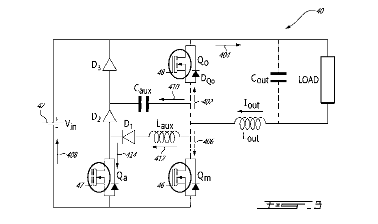
form a filter that averages a voltage across an opposite diode D0, which is
described hereinbelow, so that a voltage on the LOAD remains fairly constant.
[0004] The circuit 20 includes a commutation cell and a control
component (described in details hereinbelow) and controls the voltage applied
to the LOAD by the source 22. The commutation cell of the circuit 20
comprises a main switch Qm, which may for example consist of a MOSFET or
like power electronic switch, controlled by a gate driver (not shown but shown
on Figure 1), and the opposite diode D0. The commutation cell further includes
an equivalent source capacitor (not shown) in parallel with the source 22 and
an equivalent current source (not specifically shown) for a current /out that
flows
in the LOAD.
[0005] When the main switch Qm is open, the current /out flows from
the LOAD through the opposite diode D, and returns to the LOAD, as reflected
by the arrows 202 and 204. When the main switch Qm is closed, the current /out
flows through the main switch Qm and the source 22 and returns to the LOAD,
as reflected by the arrows 206, 208 and again 204. When the main switch Qm
is closed, a voltage between its drain and source is zero (or substantially
zero)
and the entire voltage Vm, for example 450 Volts DC, is applied across the
opposite diode D0. It is however intended to use the circuit of Figure 2 to
apply
a controlled DC voltage to the LOAD, this controlled DC voltage being lower
than the voltage Vm of the source 22. To this end, the commutation cell is
switched on and off at a rapid rate, a duty cycle of the commutation cell
controlling an effective voltage applied to the LOAD. The voltage applied on
the LOAD is equal to the duty cycle multiplied by the voltage VII, of the
source
22.
CA 02991323 2018-01-04
WO 2017/004700
PCT/CA2016/050761
3
[0006] The auxiliary components of the circuit 20 comprise an
auxiliary capacitor Caõ, an auxiliary inductor Laõ, diodes D1, D2 and D3, as
well
as an auxiliary switch Qa. Initially, when the main switch Qm is conducting
the
entire current /out (see arrow 206) the voltage between its drain and source
is
zero. At that time, a voltage on the auxiliary capacitor Caõ is substantially
equal to VII,. Opening the main switch Qm, the current lout is gradually
deviated
in the auxiliary capacitor Caõ, arrow 210. Accordingly, the voltage slope is
limited and therefore allows Om to turn-off at almost zero voltage, thereby
reducing switching losses in the main switch Qm.
[0007] Then, while the main switch Qm is off, the auxiliary switch Qa,
for example another MOSFET, is closed in preparation for closing the main
switch Qm again. The voltage that was applied across the auxiliary switch Qa
is
gradually deviated across the auxiliary inductor Law,. Accordingly, the
current
slope is limited and therefore allows Qa to turn-on at almost zero current,
thereby reducing switching losses in the auxiliary switch Qa.
[0008] A portion of the current lout is now directed via the auxiliary
inductor Laõ to this auxiliary switch Qa, see arrows 212 and 214. The
auxiliary
inductor Laõ limits the voltage across the auxiliary switch Qa in order to
minimize switching losses. As a voltage across the auxiliary switch Qa
decreases, while it becomes closed, its current variation di/dt increases,
causing a voltage across the auxiliary inductor Laõ to also increase. At the
time when the auxiliary switch Qa becomes fully conductive (i.e. when it is
fully
closed), the voltage VII, is substantially present on the auxiliary inductor
Laõ
and the current variation di/dt becomes equal to V,, divided by the value of
the
auxiliary inductor Laõ. Until this moment, at least a part of the current lout
was
flowing through the opposite diode D0, along arrow 202, on which a voltage is
initially at or near zero. When the entire current lout flows through the
auxiliary
switch Qa, arrow 214, a recovery current starts flowing in reverse direction
in
the opposite diode D,, in a direction opposite to that of arrow 202. This
CA 02991323 2018-01-04
WO 2017/004700
PCT/CA2016/050761
4
recovery current in the opposite diode D, has a rate of V,, divided by Laõ.
Rapidly, once charges accumulated on the PN junction of the opposite diode
D, are withdrawn, the opposite diode D, becomes blocked and a resonance is
initiated between the auxiliary inductor Laõ and parasitic capacitances (not
shown) of the opposite diode D,, of the main switch Qm and of another diode
D2 through the auxiliary capacitor Caw,. It is observed that the auxiliary
capacitor Caõ is much larger than the parasitic capacitance of the diode D2.
Energy accumulated in these capacitors is transferred to the auxiliary
inductor
Laux after a quarter of a resonant cycle.
[0009] Because the opposite diode D, is now blocked and because a
resonance with the above mentioned capacitors has taken place for quarter of
a cycle, a voltage thereacross is equal to VII,. A voltage on the main switch
Qm
is therefore zero, allowing closing of this main switch Qm at zero voltage.
The
auxiliary switch Qa is then opened in order to limit losses in the auxiliary
inductor Laux. The current that was flowing in the auxiliary switch Qa is
gradually deviated to the auxiliary capacitor Caux. Accordingly, the voltage
slope is limited and therefore allows Qa to turn-off at almost zero voltage,
thereby reducing switching losses in the auxiliary switch Qa, thereby reducing
switching losses in the auxiliary switch Qa. As expressed hereinabove, charges
accumulated on the auxiliary capacitor Caux will be transferred to the main
switch Qm when this latter switch opens, in another cycle. No significant
energy
is spent in the auxiliary capacitor Caux. This current in the auxiliary
inductance
reaches zero after a time dictated by the current that flows therein upon
opening of switch Qa and a current variation in the auxiliary inductance di/dt
that defined as the source voltage V,, divided by the auxiliary inductor Laux.
[0010] Upon opening of the auxiliary switch Qa, due to the current
variation di/dt in the diode D1 at a rate of V,, divided by Laux, there will
be a
recovery current in the diode D1, which is in series with the auxiliary
inductor
Laux. Another recovery current will also be present in the diode D3, but it
will be
CA 02991323 2018-01-04
WO 2017/004700
PCT/CA2016/050761
very small because the auxiliary capacitor Caw( is large. The voltage across
the
diode D3 remains near zero. Yet another recovery current in the diode D2 will
be very small because an output capacitance Coss of the auxiliary switch Qa is
large compared to the parasitic capacitance of the diode D1 and further
because the diode D2 is smaller than the diode D1. These recovery currents
are however of secondary importance because the diodes D2 and D3 are much
smaller than the opposite diode D,. The diode D1 provides a soft recovery
because it is larger than the diodes D2 and D3 and because, as mentioned
hereinabove it turns off with the current variation di/dt at a rate of V,,
divided by
Laux=
[0011] Those familiar with the circuit 20 will appreciate that it can
be
operated at a duty cycle in a range from zero to 100 percent, wherein the duty
cycle is defined as a ratio of the closing time of the switches over a
complete
cycle time of the commutation cell. It is however required to allow full
closing of
the switches when the duty cycle is greater than zero. It is also required to
prevent opening of the switches if the duty cycle is so great that the
auxiliary
capacitor Caux is prevented from fully discharging upon opening of the main
switch Qm.
[0012] The circuit 20 of Figure 2 suffers from the following
drawbacks.
[0013] Firstly, the recovery current in the opposite diode D0, which
is
a large diode and, in case of a full leg, the very slow parasitic diode of a
MOSFET, generates significant losses occurring in the circuit 20, primarily in
the diode itself and in the auxiliary inductor Laux as well as in the
auxiliary
switch Qa due to the recovery current before added to the load current. These
losses impact the efficiency of the circuit 20 and limit the switching
frequency.
The losses generate heat that must in most cases be dissipated, cumulated
with the limited switching frequency, which in turn impact the physical size
of a
converter built on the basis of the circuit 20.
CA 02991323 2018-01-04
WO 2017/004700
PCT/CA2016/050761
6
[0014] Secondly, the resonance between various elements of the
circuit 20, in particular at the time of blocking the opposite diode D0, when
the
recovery current causes a very high dV/dt across the parasitic capacitance of
the opposite diode D0, causes significant noise in terms of electromagnetic
interference (EMI). This EMI may be detrimental to many applications and may
require complex filtering, which in turn may involve an increase of the size
and/or cost of the physical implementation of the circuit 20, or a decrease of
its
performance, or both.
[0015] Finally, the energy flow may only circulates from the high
voltage to the low voltage (unidirectional from input to output) so it can
only be
used has a DC/DC buck converter.
[0016] Therefore, there is a need for improvements to converter
circuits that compensate for problems related to poor efficiency and
electromagnetic noise generation in power electronics circuits and to improve
the flexibility to allows the operation as DC/DC boost converter, as DC/AC
converter or as AC/DC converter.
SUMMARY
[0017] According to the present disclosure, there is provided a
circuit
for providing a current from a source to a load. A commutation cell includes a
main switch that controls a voltage applied by the source to the load. An
opposite switch maintains the current in the load when the load is
disconnected from the source by the main switch. The opposite switch returns
the load current to the main switch when the main switch connects again the
load to the source. A synchronizing controller controls opening and closing
sequences of the main switch and of the opposite switch.
[0018] According to the present disclosure, there is also provided a
DC-DC converter implemented using the circuit for providing a current from a
source to a load.
CA 02991323 2018-01-04
WO 2017/004700
PCT/CA2016/050761
7
[0019] The present disclosure further relates to a DC to AC converter
implemented using the circuit for providing a current from a source to a load
and a peer commutation cell. The opposite switch is used as a peer main
switch of the peer commutation cell while the main switch is used as a peer
opposite switch of the peer commutation cell. The synchronizing controller
controls opening and closing sequences of the main switch, of the peer main
switch, of the opposite switch and of the peer opposite switch so that the
current flowing in the load is an alternative current.
[0020] The foregoing and other features will become more apparent
upon reading of the following non-restrictive description of illustrative
embodiments thereof, given by way of example only with reference to the
accompanying drawings.
BRIEF DESCRIPTION OF THE DRAWINGS
[0021] Embodiments of the disclosure will be described by way of
example only with reference to the accompanying drawings, in which:
[0022] Figure 1 is a schematic representation of a MOSFET with its
parasitic elements and its gate driver;
[0023] Figure 2 is a circuit diagram of a conventional MOSFET-based
DC-DC Buck converter;
[0024] Figure 3 is a circuit diagram of a soft switching synchronized
DC-DC buck converter according to an embodiment;
[0025] Figure 4 is a timing diagram showing operations leading to
turning on the main switch of the circuit of Figure 3 and an
impact of those operations on a current in the auxiliary
inductor;
[0026] Figure 5 is a schematic diagram of a gate driver circuit for
controlling the switches of the circuit of Figure 3; and
CA 02991323 2018-01-04
WO 2017/004700
PCT/CA2016/050761
8
[0027] Figure 6 is a circuit diagram of a soft switching synchronized
DC-AC converter according to another embodiment.
[0028] Like numerals represent like features on the various drawings.
DETAILED DESCRIPTION
[0029] Various aspects of the present disclosure generally address
one or more of the problems related to the generally poor efficiency and to
the
electromagnetic noise generation in power electronics circuits.
[0030] In a switching circuit that includes a commutation cell, these
problems are alleviated by replacing an opposite diode, conventionally used to
maintain a freewheeling current in a load when a main switch of the
commutation cell is opened (non-conductive), by an opposite switch. The large
size of the opposite diode causes a large amount of recovery current when the
main switch starts conducting again, in turn causing important switching
losses
and electromagnetic noise. In contrast, the present disclosure proposes to
replace the opposite diode by a switch (Qo) that can be controlled in
synchrony
with the main switch to carry the freewheeling load current until the load
current is completely deviated from the opposite switch to the auxiliary
switch.
The opposite switch is fully opened with a minimum of the remaining charges
to be recovered, and to gradually, in a resonant manner, reduce the voltage
across the main switch to turn it on at zero voltage; the main switch is
conducting the full load current again. This synchronization of the main
switch
and of the opposite switch softens the overall behavior of the circuit upon
switching, reducing switching losses of the opposite diode, in turn reducing
switching losses and electromagnetic losses.
[0031] The disclosed circuit can be used as a DC-DC voltage
converter. A DC-AC converter, also called inverter, can be obtained by
combining two commutation cells of opposite polarities as will be described
herein.
CA 02991323 2018-01-04
WO 2017/004700
PCT/CA2016/050761
9
[0032] The following terminology is used throughout the present
disclosure:
[0033] Softening: reduction of transient effects, dl/dt and dV/dt,
upon
switching in a circuit.
[0034] Commutation cell: an assembly of electronic components
connected to a voltage source that alternatively supplies
current to a current source and allow freewheel of this a
current source connected to a load.
[0035] Switch: a power electronic switch that is forced opened and
forced closed.
[0036] Main switch: switch of the commutation cell that passes
current from the voltage source to the current source when is
conductive or from the current source to the voltage source.
[0037] Auxiliary switch: switch in parallel with the main switch and
in
series with an auxiliary inductance, the auxiliary switch being
arranged to turn-on at almost zero current before the main
switch.
[0038] Opposite switch: a switch that is in parallel with the diode of
the commutation cell and that takes the load current when the
main switch is not conductive.
[0039] Controller: a processor, computer, FPGA, CPLD, DSP, CPU,
or a combination of any number of these components, possibly
including a memory, an interface, an analog to digital
converter, and similar components, the controller may be hard-
wired for carrying a function or may comprise programmable
code for carrying a function.
[0040] Synchronizing controller: a controller that gives commands to
the switches, via respective gate drivers, to control opening
CA 02991323 2018-01-04
WO 2017/004700
PCT/CA2016/050761
and closing sequences of the switches in a synchronized
manner.
[0041] Auxiliary capacitor, auxiliary inductor and auxiliary diodes:
components of the commutation cell, distinct from components
of the load, used to deviate current and/or voltage during
commutations.
[0042] Zero voltage: In the present disclosure, a 'zero voltage' on a
component such as a diode or a switch indicates that this
component is conductive. In practice, the voltage on this
component may be slightly greater than zero volts while still
being significantly less than a voltage of the power source or
than a load voltage. Expressions 'zero voltage' and equivalent
are used in order to simplify the present disclosure and are not
to be construed in the absolute.
[0043] Zero current: In the present disclosure, a 'zero current' on a
component such as a diode or a switch indicates that this
component is not conductive. In practice, there is always a
small current often called leakage current. Expressions 'zero
current' and equivalent are used in order to simplify the
present disclosure and are not to be construed in the absolute.
[0044] Referring now to the drawings, Figure 3 is a circuit diagram of
a soft switching synchronized DC-DC converter according to an illustrative
embodiment. In the circuit 40, power from a source 42 having a voltage V,, is
converted to another DC voltage applied to a load (shown as LOAD on Figure
3). The LOAD may consist of a purely resistive element or may also include
capacitive and/or inductive components. A capacitor C0ut placed in parallel
with
the LOAD and an inductor Lut placed in series with the LOAD form a filter that
averages a voltage as will be described hereinbelow.
CA 02991323 2018-01-04
WO 2017/004700
PCT/CA2016/050761
11
[0045] The circuit 40 differs from the circuit 20 of Figure 2 mainly
in
that the opposite diode D, of the circuit 20 is replaced by another controlled
power electronic switch, opposite switch Q0, which has its own parasitic diode
DQ0 This modification to the conventional circuit 20 of Figure 2 brings
important changes to its behavior. The main switch Qm, the auxiliary switch Qa
and the opposite switch Q, have respective gates 46, 47 and 48 connected to
respective gate drivers (shown on Figure 5) to control their opening and
closing.
[0046] The circuit 40 includes a commutation cell and a control
component (described in details hereinbelow) and controls the voltage applied
to the LOAD by the source 42. The commutation cell of the circuit 40 includes
a main switch Qm, which may for example consist of a MOSFET or like power
electronic switch, controlled by a gate driver (not shown but shown on Figure
1). The opposite diode D, of Figure 2 is replaced with the opposite switch Q,
in
the commutation cell of the circuit 40. The commutation cell further includes
an
equivalent source capacitor (not shown) in parallel with the source 42 and the
inductor Lout, which represents an equivalent load inductance for a current
/out
that flows in the LOAD.
[0047] When the main switch Qm is open, the current /out flows from
the LOAD through the opposite switch Q, controlled by a gate driver and
returns to the LOAD, as reflected by the arrows 402 and 404. When the main
switch Qm is closed, the current /out flows through the main switch Qm and the
source 42 and returns to the LOAD, as reflected by the arrows 406, 408 and
again 404. When the main switch Qm is closed, a voltage between its drain and
source is zero and the entire voltage V,õ, for example 450 Volts DC, is
applied
across the opposite switch Q0. It is however intended to use the circuit of
Figure 3 to apply a controlled DC voltage to the LOAD, this controlled DC
voltage being lower than the voltage V,, of the source 42 by a factor equal to
a
duty cycle of the circuit 40. To this end, the commutation cell is switched on
CA 02991323 2018-01-04
WO 2017/004700
PCT/CA2016/050761
12
and off at a rapid rate in order to control an effective voltage applied to
the
LOAD. The commutation cell may be cycled at a rapid rate, for example at 300
KHz.
[0048] The auxiliary components of the circuit 40 comprises an
auxiliary capacitor Caux, an auxiliary inductor Laux, auxiliary diodes D1, D2
and
D3, as well as an auxiliary switch Qa, which may be another MOSFET or like
power electronic switch. Initially, when the main switch Qm is conducting the
entire current /out, see arrow 406, the voltage between its drain and source
is
zero. Opening the main switch Qm, the current /out is gradually deviated in
the
auxiliary capacitor Caux, arrow 410, which discharges from the voltage V,, to
zero. As mentioned hereinabove, the voltage slope is limited and therefore
allows Qm to turn-off at almost zero voltage, thereby reducing switching
losses
in the main switch Qm
[0049] The parasitic diode DQ0 of the opposite switch Q, starts to
take
the load current. The opposite switch Q, then starts to close at zero voltage
in
order to reduce conduction losses in its parasitic diode DQ0, eliminate the
switching losses and to limit charges accumulated on its PN junction in view
of
its later opening. At the same time, the inductor Lut causes the current /out
to
remain substantially constant during the opening of the main switch Qm.
Following opening of the main switch Qm, the current /out is now flowing in
the
opposite switch Q0, along arrow 402, before returning to the LOAD, arrow 404.
The voltage drop across Qo does allow a small current to circulate in Do.
[0050] Then, while the main switch Qm is off, the auxiliary switch Qa
is
closed in preparation for closing the main switch Qm again. A portion of the
current /out is now directed via the auxiliary inductor Laux to this auxiliary
switch
Qa, see arrows 412 and 414. The auxiliary inductor Laux limits the flow of
current through the auxiliary switch Qa during the transition of its drain to
source voltage from V,, to zero in order to minimize switching losses. As a
voltage across the auxiliary switch Qa decreases, while it turns on, its
current
CA 02991323 2018-01-04
WO 2017/004700
PCT/CA2016/050761
13
variation di/dt increases, causing a voltage across the auxiliary inductor Laõ
to
also increase. At the time when the auxiliary switch Qa becomes fully
conductive (i.e. when it is fully closed), the full voltage VII, is present on
the
auxiliary inductor Laõ and the current variation di/dt becomes equal to VII,
divided by the value of the auxiliary inductor Lau,. Until this moment, at
least a
part of the current lout was flowing through the opposite switch Q0, along
arrow
402, on which a voltage is initially at or near zero. Once the entire current
/00t
flows in the auxiliary switch Qa, arrow 414, the current in the opposite
switch
Q, begins to flow in a reverse direction, which is opposite to the direction
of the
arrow 402. Because a drain to source resistance of the opposite switch Q, is
very low when closed, very little current was flowing in its parasitic diode
DQ0
while it was closed and, consequently, very few charges were accumulated on
its PN junction. Current that is now flowing in the reverse direction in the
opposite switch Q0, opposite to the direction of the arrow 402, removes the
remaining charges and completely blocks its parasitic diode DQ0. Opening the
opposite switch Q, under a low current condition, for example at 15% of the
rated current for the LOAD, limits the switching losses of the opposite switch
Q, and significantly reduces the switching losses of its parasitic diode DQ0,
also
reducing associated electromagnetic noise. This is achieved by using a precise
triggering time for the opposite switch Q0, for example with a resolution of
about 10 nsec. In this manner, significant current and losses, important noise
and long switching times in the auxiliary switch Qa due to its own slow
parasitic
diode can be alleviated. It may be observed that reverse current in the
opposite switch Q, is lower than an equivalent recovery current of a diode
that
is conventionally used.
[0051] Some resonance is initiated between the auxiliary inductor Laõ
and parasitic capacitances (not shown) of the opposite switch Q0, of the main
switch Qm and of another diode D2 through the auxiliary capacitor Caõ. It is
observed that the auxiliary capacitor Caõ is much larger than the parasitic
capacitance of the diode D2. Energy accumulated in these capacitors is
CA 02991323 2018-01-04
WO 2017/004700
PCT/CA2016/050761
14
transferred to the auxiliary inductor Laõ after a quarter of a resonant cycle.
The
voltage across Caux should remain near zero to limit the voltage across Qa
upon turn-off.
[0052] Because the opposite switch Q, is now opened, a voltage
thereacross is equal to VII,. A voltage on the main switch Qm is therefore
zero,
allowing closing of this main switch Qm at zero voltage without any
significant
turn-on losses. The auxiliary switch Qa is then opened in order to limit
losses in
the auxiliary inductor Law,. Opening the auxiliary switch Qa, the current in
Qa is
gradually deviated in the auxiliary capacitor Caux, reverse of arrow 210.
Accordingly, the voltage slope is limited and therefore allows Qa to turn-off
at
almost zero voltage, thereby reducing switching losses in the auxiliary switch
Qa. . As expressed hereinabove, charges accumulated on the auxiliary
capacitor Caux will be transferred to the main switch Qm when this latter
switch
opens, in another cycle of the circuit 40. No significant energy is dissipated
in
the auxiliary capacitor Caux. The current in the auxiliary switch Qa is
deviated in
the diodes D2 and D3. The current in the auxiliary inductor Laux reaches zero
after a time dictated by current variation di/dt of VII, divided Laux.
[0053] Due to current variation di/dt in the auxiliary inductor Laux,
there
will be a recovery current in a diode D1, which is in series with the
auxiliary
inductor Laux. Another recovery current will also be present in a diode D3,
but it
will be very small because the auxiliary capacitor Caux is large. Yet another
recovery current in the diode D2 will be very small because an output
capacitance Coss of the auxiliary switch Qa is large and further because the
diode D2 is smaller than the diode D1. These recovery currents are however of
secondary importance because the diodes D2 and D3 are much smaller than
the parasitic diode DQ0 of the opposite switch Q0. The diode D1 provides a
soft
recovery because it is larger than the diodes D2 and D3 and because, as
mentioned hereinabove it turns off with the current variation di/dt at a rate
of
Vm divided by Laux.
CA 02991323 2018-01-04
WO 2017/004700
PCT/CA2016/050761
[0054] The main switch Qm, the auxiliary switch Qa and the opposite
switch Q, may each comprise a MOSFET, a junction field effect transistor
(JFET) including a silicon carbide (SiC) or a gallium nitride (GaN) JFET, or
another type of power electronic switch. The various switches of the circuit
40
may be of different types. Each switch may also include an insulated-gate
bipolar transistor (IGBT) used in parallel with an associated diode, as
conventional IGBTs do not comprise any significant intrinsic diodes.
[0055] Figure 4 is a timing diagram showing operations leading to
turning on the main switch of the circuit of Figure 3 and an impact of those
operations on a current in the auxiliary inductor. A timing diagram 50 shows a
varying current 52 in the auxiliary inductor Laõ as a function opening and
closing sequences of the main switch Qm (sequence 54), of the auxiliary switch
Qa (sequence 56) and of the opposite switch Q, (sequence 58). These latter
sequences 54, 56 and 58 are expressed in terms of gate to source voltages
(Vg,) applied to each of the switches. It will be understood that the switches
are
conductive when the lines of the sequences 54, 56 and 58 represent high Vg,
voltages (lines are high) and not conductive when the Vg, voltages are low
(lines are low). For example, the opposite switch Q, is initially conductive
until
a time t3, as illustrated by the sequence 58. A gate driver circuit (shown on
Figure 5) controls the closing time of the switches Qa, Q, and Qm.
[0056] Initially, before time to, the opposite switch Q, is the sole
conducting switch, as reflected by the dotted line extending the sequence 58
on the left of the timing diagram 50, before the time to, and the current /out
is
freewheeling between the LOAD and the opposite switch Q0, flowing from the
source to the drain in the opposite switch Q,, see arrows 402 and 404 on
Figure 3. The auxiliary switch Qa is closed at time to and its voltage starts
to
decrease. A value of the time to when the auxiliary switch Qa is closed is
used
to calculate the current 52 in the auxiliary inductor Laõ. Then, considering a
constant and gradual decrease of a drain to source voltage across the
auxiliary
CA 02991323 2018-01-04
WO 2017/004700
PCT/CA2016/050761
16
switch Qa, the voltage across the auxiliary inductor Laõ increases gradually
to
reach the voltage Va, of the source 42 at the time t1, at which time the drain
to
source voltage of the auxiliary switch Qa falls to zero. The current 52 at the
time t1 (Iti) can be calculated using equation (1):
/ t (1)
t1=1.01 Lalux. Vtlin't)dt 217* Lna* Ut 1X
[0057] The time duration from to to t1 may be approximated as a
constant because it is substantially independent of the load current, only
depending on the voltage I/Th. In practice, it has been found that a 20%
difference of the voltage Va, has little effect on the current 52 and on the
time
[0058] The current 52 in the auxiliary inductor Laõ continues to
increase with a slope of Va, divided by Laõ and reaches a value of the current
/out in the LOAD at a time t2. The calculation of the time duration between t2
and t1 can be calculated using equation (2):
t2 ¨ t1 = Laux * lout jt (2)
Vin
[0059] The opposite switch Q, is maintained conductive for a brief
period in a range of about 5 to 15 nsec, for example for 10 nsec after t2,
until a
reversal of the current in the opposite switch Q0, now flowing from the drain
to
the source at a time t3. The above mentioned resonance between the auxiliary
inductor Laõ and the various parasitic capacitances of the circuit 40 is
initiated
at the time t3, after opening of the opposite switch Q0, and lasts for up to a
quarter of a cycle until a time t4. The added current will have a slope of Va,
divided by Laõ and a duration t4 - t3 of up to about 55 nsec. This current and
a
very low recovery current of the parasitic diode DQ0 add to the current 52 in
auxiliary inductor Laõ such that the current 52 overshoots above the value of
the current /out. A proper timing for opening the opposite switch Q, is
effective
in reducing electromagnetic noise and switching losses in the parasitic diode
DQ0, as long as the additional current, for example 450 volts over an
CA 02991323 2018-01-04
WO 2017/004700
PCT/CA2016/050761
17
inductance of 5 pH, or 0.9 amperes, remains below the maximum reverse
recovery current of a standard diode.
[0060] The main switch Qm can be closed shortly after the overshoot,
at time t5, for example 10 nsec after the time t4. Soon thereafter, for
example
after another delay of about 50 nsec until a time to, the auxiliary switch Qa
is
opened and its current is being deviated in the auxiliary capacitor Caõ that
is
charged up to VII,. The drain to source voltage of the auxiliary switch Qa
increases and, consequently, so does the voltage across the auxiliary
inductance Laõ and across the auxiliary capacitor Caõ. The current 52 in the
auxiliary inductance Laõ starts to decrease with a slope dictated by its
voltage.
Once the voltage across the auxiliary switch Qa reaches V,õ, at a time t7, the
slope of the current in the auxiliary inductor Laõ becomes -V,õ, divided by
Lau,.
The current in the auxiliary inductor Laõ reaches zero at a time to.
[0061] In the example of Figure 4, the current 52 reaches 2.3 A at a
time t1 of 50 nsec (i.e. 50 nsec after to) and has an overshoot of at least
6.4 A
between t3 and t4. The magnitude of the current 52 at time t1, which is 2.3 A,
is
essentially a function of this 50 nsec time duration and of a value the
auxiliary
inductor Laõ, which is set to 5 pH (microHenries) in the example of Figure 4.
The voltage VII, and the current lout have little impact of the amount of
current
52 at time t1. These and other numerical values expressed in the description
of
the example of Figure 4 are for illustration only and do not limit the present
disclosure.
[0062] A span between times t3 and t4 up to about 55 nsec in the
example of Figure 4. This value corresponds to a quarter of 4.5 MHz natural
resonant frequency between the auxiliary inductor Laõ and the parasitic
capacities of the switches Qm and Q0.
[0063] A span between times t7 and to can be estimated as a peak
value of the current 52 times the value of the auxiliary inductor Laõ divided
by
VII,. The time to defines a minimum pulse width for the circuit 40. The main
CA 02991323 2018-01-04
WO 2017/004700
PCT/CA2016/050761
18
switch Qm should not be opened before that time. Starting from the time t8 the
main switch Qm may be opened if the resulting duty cycle provides the desired
voltage across the LOAD.
[0064] Under low current /out conditions, the timing of opening and
closing of the various switches of the circuit 40 may be such that a
discontinuous mode in obtained, in which current stops completely in the
output inductance if the opposite switch Q, is kept open during the
freewheeling period. In fact, under this condition, the opposite switch Q, is
not
closed because the reverse current in its parasitic diode DQ0 has a very low
current variation di/dt, determined by a voltage on the LOAD divided by a
value
of the inductor Lout. Consequently, the parasitic diode DQ0 has a low recovery
current and generates few losses or stray EMI noise.
[0065] Figure 5 is a schematic diagram of a gate driver circuit for
controlling the switches of the circuit of Figure 3. In a gate driver circuit
60,
three (3) gate drivers 62, 64 and 66 are each dedicated to distinct switches,
being respectively connected to the gate 46 of the main switch Qm, to the gate
47 of the auxiliary switch Qa, and to the gate 48 of the opposite switch Q0. A
synchronizing controller 68 provides signals to the gate drivers 62, 64 and 66
to control opening and closing sequences of the switches. The synchronizing
controller 68 sets a time to for initiating a cycle of the circuit 40 and
internally
stores a value for the time t1 as a constant. The synchronizing controller 68
implements real-time calculations of equations (1) and (2) to determine a
value
for the time t3, when the opposite switch Q, opens. Value to the time t5 when
the main switch Qm is closed and of the time to when the auxiliary switch Qa
is
open does not need to be calculated but may instead be assessed from tables
based on the current /out and the input voltage VII,. The synchronizing
controller
68 also controls the duty cycle of the circuit 40, effectively controlling the
voltage applied to the LOAD.
CA 02991323 2018-01-04
WO 2017/004700
PCT/CA2016/050761
19
[0066] The synchronizing controller 68 performs its calculations at a
rapid rate, for example at a rate of 500 kHz, in order to update the timing
according to the output current /out. Furthermore, the controller should have
the
ability to respond with a sufficient resolution in the order of about 10 nsec
which is on the order of about 0.5 % of the full cycle. Without limitation,
the
synchronizing controller 68 may be implemented using one or more Field
Programmable Gate Arrays (FPGA), Digital Signal Processors (DSP),
Application Specific Integrated Circuits (ASIC), or any combination of such
devices.
[0067] The opposite diode D, of the DC-DC converter introduced in
the foregoing description of Figure 2 needs to be replaced with a switch when
implementing a full leg configuration having two (2) commutation cells forming
for example a DC-AC converter. In fact, when MOSFET technology is used,
the choice of opposite diodes is limited to the parasitic diode of the
opposite
MOSFET switch. These parasitic diodes are notoriously slow, which
exacerbates the problems related to recovery current.
[0068] The opposite switch Q, of the circuit 40 may be further used as
a main switch for an added commutation cell. Figure 6 is a circuit diagram of
a
soft switching synchronized DC-AC converter according to another
embodiment. A circuit 70 includes a source 72 and combination 74 including a
commutation cell and an auxiliary circuit, as described in the foregoing
description of Figure 3. The circuit 70 adds a further combination 76
including
a peer commutation cell and auxiliary circuit, the combination 76 having a
reverse polarity. The commutation cell of the combination 74 is, in the
context
of the circuit 70, a low' commutation cell while the peer commutation cell is
a
'high' commutation cell. A peer auxiliary switch QaH has, in the high
commutation cell, the same function as the auxiliary switch Qa of the low
commutation cell. Likewise, peer diodes DiH, D2H, D3H, a peer auxiliary
inductor
L1auxH and a peer auxiliary capacity CauxH respectively play the same roles in
CA 02991323 2018-01-04
WO 2017/004700
PCT/CA2016/050761
the high commutation cell as the diodes D1, D2, D3, the auxiliary inductor
Liaõ
and the auxiliary capacity Caõ of the low commutation cell.
[0069] The opposite switch Q, introduced in the foregoing description
of Figure 3 still has the same function in the low commutation cell and is
further
used as a peer main switch Qinfi in the high commutation cell. Likewise, the
main switch Qm of the low commutation cell is also used as a peer opposite
switch Qopi for operation of the high commutation cell.
[0070] In one operating phase of the circuit 70, the current /out
flows in
the direction indicated by the arrow above the inductor Lout, through the main
switch Qm of the low commutation cell and to the source 72. In another
operating phase of the circuit 70, the current /out flows in the opposite
direction,
from the source 72 and through the peer main switch QmH. As a result, the
current /out flowing through the LOAD is an alternative current in the circuit
70.
Phase transitions for each of the commutation cells are handled in the same
manner as described hereinabove. The gate driver circuit 60 of Figure 5 may
be extended with an additional gate driver (not shown) to also control the
gate
of the auxiliary switch QaH=
[0071] Those of ordinary skill in the art will realize that the
description
of the circuits for softening switching phases in voltage converters are
illustrative only and are not intended to be in any way limiting. Other
embodiments will readily suggest themselves to such persons with ordinary
skill in the art having the benefit of the present disclosure. Furthermore,
the
disclosed circuits may be customized to offer valuable solutions to existing
needs and problems related to poor efficiency and electromagnetic noise
generation in power electronics circuits.
[0072] It should be observed that, in the case of other power
electronic switch types, for example bipolar transistors, the term "gate" may
be
replaced with "base", the base being controlled by a current as opposed to the
CA 02991323 2018-01-04
WO 2017/004700
PCT/CA2016/050761
21
gate that is controlled by a voltage. These distinctions do not change the
overall operation principles described hereinabove.
[0073] In the interest of clarity, not all of the routine features of
the
implementations of the circuits are shown and described. It will, of course,
be
appreciated that in the development of any such actual implementation of the
circuits, numerous implementation-specific decisions may need to be made in
order to achieve the developer's specific goals, such as compliance with
application-, system-, and business-related constraints, and that these
specific
goals will vary from one implementation to another and from one developer to
another. Moreover, it will be appreciated that a development effort might be
complex and time-consuming, but would nevertheless be a routine undertaking
of engineering for those of ordinary skill in the field of power electronics
having
the benefit of the present disclosure.
[0074] The present disclosure has been described in the foregoing
specification by means of non-restrictive illustrative embodiments provided as
examples. These illustrative embodiments may be modified at will. The scope
of the claims should not be limited by the embodiments set forth in the
examples, but should be given the broadest interpretation consistent with the
description as a whole.