Note : Les descriptions sont présentées dans la langue officielle dans laquelle elles ont été soumises.
ENCODED BIOSENSORS AND METHODS OF MANUFACTURE
AND USE THEREOF
[001]
TECHNICAL FIELD
(002] The present invention relates generally to an analyte test sensor for
use in
measuring concentrations of an analyte in a biological fluid and, more
particularly, to an
analyte test strip having coding information formed thereon.
BACKGROUND
[003] Biosensors provide an analysis of a biological fluid, such as whole
blood, urine,
or saliva. Measuring the concentration of substances in biological fluids is
an important
tool for the diagnosis and treatment of many medical conditions. For example,
the
measurement of glucose in body fluids, such as blood, is crucial to the
effective
treatment of diabetes. The sample of biological fluid may be directly
collected or may
be a derivative of a biological fluid. Typically, biosensors have a
nondisposable
measurement device or test meter that is used to analyze the sample of
biological fluid
that is placed on the test strip.
(004] Many biosensor systems provide calibration information to the
measurement
device prior to the analysis. The measurement device typically uses this
information to
adjust the analysis of the biological fluid in response to one or more
parameters. The
accuracy and precision of the analysis is improved by using the calibration
information.
If the calibration information is not used, the measurement device may not
complete the
- 1 -
Date Recue/Date Received 2020-09-24
CA 02992283 2018-01-11
WO 2017/039976 PCT/US2016/046124
analysis or may make a wrong analysis of the concentration of the analyte in
the
biological fluid.
[005] It is common practice in such test meter/test strip systems to ensure
proper
identification of the test strip in order to ensure proper test results. For
example, a
single test meter may be able to analyze several different types of test
strips, wherein
each type of test strip is designed to test for the presence or concentration
of a different
analyte in the biological fluid. In order to properly conduct the test, the
test meter must
know which type of test is to be performed for the test strip currently in
use.
[006] Also, lot-to-lot variations in the test strips normally require
calibration
information to be loaded into the test meter in order to ensure accurate test
results. A
common practice for downloading such calibration information into the test
meter is the
use of an electronic read-only memory key (ROM key) that is inserted into a
corresponding slot or socket of the test meter. Because this calibration data
may only
be accurate for a particular production lot of test strips, the user is
usually asked to
confirm that the lot number of the test strip currently in use matches the lot
number for
which the ROM key was programmed.
(007] Many other instances in which it is desirable to have information
relating to the
test strip are known to those having skill in the art. Prior art attempts to
code
information onto the test strip for reading by the test meter have suffered
from many
problems, including a severely limited amount of information that can be coded
and the
use of relatively large amounts of test strip surface area for the information
coding
function.
(008] Thus, a system and method are needed that will allow information to be
coded
onto a biosensor for reading of the information by the test meter.
BRIEF SUMMARY
(009] One aspect of the present invention discloses an analyte test sensor
strip that
is used to measure the presence or concentration of an analyte in a fluid
sample. The
test sensor strip includes a non-conductive substrate. In addition, the test
sensor strip
includes an outer or primary resistive element formed on the non-conductive
substrate
having a first end and a second end. The primary resistive element has a
- 2 -
CA 02992283 2018-01-11
WO 2017/039976 PCT/US2016/046124
predetermined configuration, which is a serpentine configuration in one form
having a
plurality of proximal ends and a plurality of distal ends. In addition, an
inner or
secondary resistive element is also formed on the non-conductive substrate
having a
tap connected to the primary resistive element at a predetermined connection
point on
the predetermined configuration thereby defining a unique resistive path
through at least
a portion of the predetermined configuration.
(00103 The unique resistive path through the predetermined configuration has
associated therewith a resistance falling within a respective one of a
plurality of ranges
of resistances. The resistance is determined based on or as a function of a
location of
the predetermined connection point on the predetermined configuration. The
unique
resistive path is associated with an attribute of the analyte test sensor
strip. An attribute
of the strip should be broadly understood to refer to any information relating
to the strip.
such as strip type, calibration information, manufacturing information,
country
information, etc. Essentially any information pertaining to the strip which
may be
desirable to convey to a meter with which the strip is used.
(00113 In order to provide an opportunity to define the unique resistive path
from
among more than one possible unique resistive paths each having an associated
resistance correlating to a different attribute, the secondary resistive
element includes a
plurality of taps. The respective tap that is connected with the predetermined
configuration at the predetermined connection point is formed or maintained in
a closed
state and all other taps of the plurality of taps are opened or formed in an
open state.
(0012] The first end of the primary resistive element is connected with a
first contact
pad and the second end is connected with a second contact pad. The secondary
resistive element has a third end connected with a third contact pad. The
unique
resistive path runs from the third contact pad through the secondary resistive
element
and then into the primary resistive element at the predetermined connection
point and
then through at least a portion of the primary resistive element to one of the
first and
second contact pads.
(00133 Another aspect of the present invention discloses an analyte test
sensor strip
that is used to measure the concentration of an analyte in a fluid sample. The
test
sensor strip includes a non-conductive substrate. A primary resistive element
is formed
- 3 -
CA 02992283 2018-01-11
WO 2017/039976 PCT/US2016/046124
on the non-conductive substrate having a predetermined configuration with a
first end
connected with a first contact pad and a second end connected with a second
contact
pad. A secondary resistive element is also formed on the non-conductive
substrate
having a plurality of taps. One tap of the plurality of taps is connected with
the primary
resistive element at a predetermined location thereby being formed and/or
maintained in
a closed state and defining a unique resistive path through at least a portion
of the
primary resistive network. The remaining taps of the plurality of taps are
opened or
formed in an open state thereby being disconnected from the primary resistive
network.
A portion of the secondary resistive element is connected with a secondary
resistive
element contact pad.
(0014] In one form, the taps that are in the open state are ablated with a
laser. The
unique resistive path is associated with an attribute of the analyte test
sensor strip. In
one form, the attribute is associated with one or more algorithm variables,
such as slope
and/or intercept for a linear correlation algorithm, associated with the test
sensor strip.
In yet another form, the analyte test sensor strip includes an optical code
formed on the
non-conductive substrate. The optical code can contain information related to
the test
sensor strip such as a product expiration date, product identification
(countries or
regions), intercepts of blood and control solutions, strip lot identification,
and other
features. In addition, the test sensor strip can also include a first
resistance loop formed
on the non-conductive substrate comprising a first measurement sense electrode
in a
spaced apart relationship from a first measurement electrode. In one form, the
first
measurement electrode is connected with the second end of the primary
resistive
element.
(00151 Another aspect of the present invention discloses a method of forming a
biosensor test strip that is utilized to measure the concentration of an
analyte. In this
aspect, a primary resistive element is formed on a non-conductive substrate
having a
predetermined configuration including a first end and a second end. Further, a
secondary resistive element is formed on the non-conductive substrate having
at least
one tap connected to a predetermined connection location on the primary
resistive
element thereby defining a unique resistive path through at least a portion of
the primary
- 4 -
CA 02992283 2018-01-11
WO 2017/039976 PCT/US2016/046124
resistive element having associated therewith a resistance falling within a
respective
one of a plurality of ranges of resistances.
[0016] The secondary resistive element is formed to include a plurality of
taps. All of
the plurality of taps but the tap connected to the predetermined location on
the primary
resistive element are ablated thereby disconnecting the ablated taps from the
primary
resistive element. The primary resistive element includes a plurality of
predetermined
connection locations. A connection location to be connected with the tap is
selected as
a function of an attribute associated with the biosensor test strip. The
unique resistive
path through the secondary and primary resistive elements is associated with
an
attribute of the biosensor test strip. Further, each range of resistances
contained in the
plurality of ranges of resistances is associated with a unique attribute of
the biosensor
test strip.
[0017] Yet another aspect of the present invention discloses an analyte test
sensor
strip that is used to measure the concentration of an analyte. The test sensor
strip
includes a non-conductive substrate. In addition, the test sensor strip
includes means
for conducting quantitative or qualitative analysis of the analyte in a sample
of fluid. A
circuit is provided on the non-conductive substrate. The circuit includes a
conductive
primary path between a first end and a second end having a predetermined
configuration between the first and second ends. The conductive primary path
has a
resistance falling within a first predetermined range. The circuit also
includes a
conductive secondary path between the first end of the conductive primary path
and a
third end. The conductive secondary path is substantially defined by a
plurality of open
taps and a closed tap. The closed tap selectively connects the third end with
the
conductive primary path at a predetermined location thereby defining a unique
resistive
path between the first end and the third end through at least a portion of the
conductive
primary path. The unique resistive path has a second resistance falling within
a second
predetermined range.
[0018] In one form, a ratio of the first resistance and the second resistance
selectively
correlates to an attribute of the analyte test sensor strip. The first end is
connected with
a first contact pad, the second end is connected with a second contact pad,
and the
third end is connected with a third contact pad. In one form, the
predetermined
- 5 -
CA 02992283 2018-01-11
WO 2017/039976 PCT/US2016/046124
configuration comprises a serpentine configuration having a plurality of
proximal ends
and a plurality of distal ends. The closed tap is connected to a respective
proximal end
of the serpentine configuration. The tap that comprises the dosed tap is
selected as a
function of an attribute of the analyte test sensor strip.
[0019] Another aspect discloses a method for measuring a concentration of an
analyte
in a sample of fluid. The method comprises the steps of providing a test
meter;
providing a test strip, the test strip comprising: a non-conductive substrate;
a working
electrode on the non-conductive substrate connectable to the test meter; a
counter
electrode on the non-conductive substrate connectable to the test meter; a
reagent part
bridging between the working electrode and the counter electrode; a primary
resistive
element on the non-conductive substrate having a first end connectable to the
test
meter and a second end connectable to the test meter, wherein the primary
resistive
element has a predetermined configuration; and a secondary resistive element
on the
non-conductive substrate having a third end connectable to the test meter,
wherein the
secondary resistive element has a tap connected to the primary resistive
element at a
predetermined connection point on the predetermined configuration thereby
defining a
unique resistive path through at least a portion of the predetermined
configuration
having a resistance value; receiving the test strip into the test meter:
operatively
connecting the working electrode, the counter electrode, the primary resistive
element,
and the secondary resistive element with the test meter; and determining an
attribute
associated with the test strip as a function of a measurement associated with
at least
the resistance value associated with the unique resistive path.
NOM In one form, the primary resistive element has a primary element
resistance
value and the attribute is determined as a function of a resistance ratio
determined by
comparing the resistance value of the unique resistive path with the primary
element
resistance value. The test meter is adjusted to output a concentration
measurement
output associated with the analyte as a function of the attribute. In one
form, an end of
the primary resistive element is connected with the counter electrode.
(0021] Yet another aspect discloses a sensor including a non-conductive
substrate
and a circuit on the non-conductive substrate. The circuit includes a primary
resistive
element on the non-conductive substrate having a first end and a second end,
wherein
- 6 -
CA 02992283 2018-01-11
WO 2017/039976 PCT/US2016/046124
the primary resistive element has a predetermined configuration; a secondary
resistive
element on the non-conductive substrate having a plurality of taps connected
to the
primary resistive element at a plurality of predetermined connection points on
the
predetermined configuration, the plurality of predetermined connection points
defining a
plurality of unique resistive paths through at least a portion of the
predetermined
configuration; and the plurality of unique resistive paths having a plurality
of resistance
values, the plurality resistance values determined using a non-linear
distribution
function. A sensor is configured to perform at least one of quantitative and
qualitative
analysis of an analyte in a sample of fluid.
K1024 Another aspect of the present invention discloses an analyte test
sensor,
comprising a non-conductive substrate and a primary resistive element on the
non-
conductive substrate having a predetermined configuration, the predetermined
configuration having a first end connected with a first contact pad and a
second end
connected to a second contact pad. The test sensor further also includes a
secondary
resistive element on the non-conductive substrate having a plurality of taps,
wherein
one tap of the plurality of taps is connected to the primary resistive element
at a
predetermined location thereby being formed in a closed state and defining a
unique
resistive path through the primary resistive network and remaining taps of the
plurality of
taps being formed in an open state thereby being disconnected from the primary
resistive network, wherein a portion of the secondary resistive element is
connected
with a secondary resistive element contact pad, and wherein each tap of the
plurality of
taps are associated with one of a plurality of predetermined resistance
values, the
plurality of predetermined resistance values having a non-linear distribution.
(00231 Another aspect of the present invention discloses a method of forming a
circuit
on a biosensor test strip. The method comprising forming a primary resistive
element
on a non-conductive substrate having a predetermined configuration including a
first
end and a second end; and forming a secondary resistive element on the non-
conductive substrate having a plurality of taps connected to a predetermined
connection
location on the primary resistive element thereby defining a plurality of
unique resistive
paths through at least a portion of the primary resistive element, each of the
plurality of
taps having associated therewith a resistance falling within a respective one
of a
- 7 -
CA 02992283 2018-01-11
WO 2017/039976 PCT/US2016/046124
plurality of ranges of resistances, wherein each of the range of resistances
are
determined based on a non-linear distribution function.
BRIEF DESCRIPTION OF THE DRAWINGS
[0024] The invention is further elucidated in the following on the basis of an
exemplary
embodiment shown in the drawings.
[0025] Fig. 1 illustrates a test strip inserted into a test meter.
[0026] Fig. 2 is an exploded view of a representative test strip.
[0027] Fig. 3A illustrates a test strip for use in measuring the concentration
of an
analyte of interest in a biological fluid.
[0028] Figs. 3B and 3C illustrate alternative embodiments of a portion of the
test strip
illustrated in Fig. 3a.
[0029] Fig. 4 illustrates a portion of the test strip illustrated in Fig. 3a.
[0030] Figs. 5A-G illustrate a portion of the test strip illustrated in Fig.
3a having a
plurality of ablated taps.
[0031] Fig. 6 illustrates another representative test strip for use in
measuring the
concentration of an analyte of interest in a biological fluid.
[0032] Fig. 7 illustrates another representative test strip for use in
measuring the
concentration of an analyte of interest in a biological fluid.
[0033] Fig. 8 illustrates another representative test strip for use in
measuring the
concentration of an analyte of interest in a biological fluid.
[0034] Fig. 9 illustrates a portion of another representative test strip for
use in
measuring the concentration of an analyte of interest in a biological fluid.
[0035] Fig. 10 is a flow diagram of a representative process used to measure
an
analyte in a biological fluid.
[0036] Fig. 11 illustrates a two encoding resistor network.
[0037] Fig. 12 is a frequency plot illustrating a cluster of test strip
contact resistances.
[0038] Fig. 13 illustrates an exemplary test strip layout used in testing.
[0039] Fig. 14 is a shared connection and partial contact resistance
compensation
schematic between points CES and RNET.
- 8 -
CA 02992283 2018-01-11
WO 2017/039976 PCT/US2016/046124
[0040] Fig. 15 is a shared connection and partial contact resistance
compensation
schematic between points RTAP and RNET.
[0041] Figs. 16A-G illustrate a plurality of test strip configurations
representing seven
possible states having uniformly distributed resistor taps..
[0042] Fig. 17A is an example biosensor strip.
[0043] Fig. 178 illustrates the example biosensor strip of Fig. 17a in
schematic form.
[0044] Fig. 18 is a distribution plot illustrating calculated resistance
ratios (RTAP¨
RNET)/(CES¨RNET) of uniformly distributed resistor taps from 1500 pairs of
network
measurements (error bars are calculated ratios assuming a nominal conductivity
and
trace pattern with an inserted worst case 235 Ohms - simulated)
[0045] Fig. 19 illustrates the distribution of resistance ratios using
multiple distribution
methodologies.
[0046] Fig. 20 is a distribution plot illustrating distribution of resistance
in resistance
ratios in a non-linear distribution of resistance values based on the number
of possible
states.
[0047] Fig. 21 is a distribution plot comparing linear distribution of
resistance ratios to
non-linear resistance ratios.
[0048] Fig. 22 illustrates an example test strip layout using non-linear
resistance
distribution values.
[0049] Fig. 23 illustrates the possible locations of control nodes and control
points in a
test strip using non-linear resistance distribution values.
[0050] Figs. 24A-G illustrate a plurality of test strip state configurations
using non-
linear resistance distribution values.
[0051] Fig. 25 is a distribution plot illustrating a range of resistance
ratios having non-
uniformly distributed resistor taps using non-linear resistance distribution
values.
[0052] Fig. 26 is a distribution plot illustrating a range of resistance
ratios at each
state, 0-6.
[0053] Fig. 27 illustrates a possible configuration of a resistive tap circuit
allowing for
Kelvin measurements.
- 9 -
CA 02992283 2018-01-11
WO 2017/039976 PCT/US2016/046124
DETAILED DESCRIPTION
NOM For the purposes of promoting an understanding of the principles of the
invention, reference will now be made to the embodiment illustrated in the
drawings,
and specific language will be used to describe that embodiment. It will
nevertheless be
understood that no limitation of the scope of the invention is intended.
Alterations and
modifications in the illustrated device, and further applications of the
principles of the
invention as illustrated therein, as would normally occur to one skilled in
the art to which
the invention relates are contemplated, are desired to be protected. In
particular,
although the invention is discussed in terms of a blood glucose meter, it is
contemplated
that the invention can be used with devices for measuring other analytes and
other
sample types. Such alternative embodiments require certain adaptations to the
embodiments discussed herein that would be obvious to those skilled in the
art.
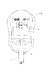
(0055] Referring to Fig. 1, a concentration measuring device or test meter 10
is
disclosed with an analyte test sensor strip 12 mounted thereto that is used to
measure
the presence or concentration of an analyte in a biological fluid, such as
whole blood,
urine, or saliva. In this form, the test strip 12 is removably inserted into a
connection
terminal 14 of the test meter 10. Upon insertion of the test strip 12, the
test meter 10 is
configured to automatically turn on and begin the measuring process, as set
forth in
greater detail below. The test meter 10 includes an electronic display 16 that
is used to
display various types of information to the user including the test results.
(0056] Referring to Fig. 2, a general test strip 12 is illustrated for
background purposes
and includes several components. The test strip 12 comprises a small body
defining a
chamber in which the sample fluid is received for testing. This sample-
receiving
chamber is filled with the sample fluid by suitable means, preferably by
capillary action,
but also optionally assisted by pressure or vacuum. The sample-receiving
chamber
includes electrodes and chemistry suitable for producing an electrochemical
signal
indicative of the analyte in the sample fluid.
(00571 In this illustrated form, the test strip 12 includes a base substrate
20, a spacing
layer 22 and a covering layer 24 comprising body cover 26 and chamber cover
28. The
spacing layer 22 includes a void portion 30 to provide a sample receiving
chamber
extending between the base substrate 20 and the covering layer 24. The base
-10-
substrate 20 carries an electrode system 32 including a plurality of
electrodes 34 and
electrode traces 36 terminating in contact pads 38. The electrodes 34 are
defined as
those portions of the electrode traces 36 that are positioned within the
sample-receiving
chamber. A suitable reagent system 40 overlies at least a portion of the
electrodes 34
within the sample-receiving chamber.
[0058] The body cover 26 and the chamber cover 28 overlying the spacing layer
22
define a slot therebetween, the slot defining a vent opening communicating
with the
sample-receiving chamber to allow air to escape the chamber as a sample fluid
enters
the chamber from the edge opening or fluid receiving opening. The test strip
12
therefore includes a dosing end 42 and a meter insertion end 44. The shape of
the
dosing end 42 is typically distinguishable from the meter insertion end 44 so
as to aid
the user. The body cover 26 and chamber cover 28 are preferably secured to the
spacing layer 22 by an adhesive layer 46. Further, a second adhesive layer 48
secures
the spacing layer 22 to the base substrate 20. A more detailed discussion of
the test
strip 12 illustrated in Fig. 2 can be found in commonly owned U.S. Patent No.
7,829,023.
[0059] Referring to Fig. 3a, a more detailed image of one preferred form of a
test strip
50 that is configured for use with the test meter 10 is illustrated having
spacer, covering
and adhesive layers removed to reveal the electrode system 32 of the test
strip 50. The
test strip 50 includes a non-conductive base substrate 52 having formed
thereon a
plurality of electrodes, traces and contact pads, as will be discussed in
greater detail
below. Such formation may be achieved by using any of a number of known
techniques, such as screen printing, lithography, laser scribing or laser
ablation. For
purposes of illustration, formation using a broad field laser ablation
technique is
generally described herein.
[0060] Prior to formation of the electrodes, traces and contact pads, the non-
conductive substrate is coated on its top surface with a conductive layer (by
sputtering
or vapor deposition, for example). The electrodes, traces and contact pads are
then
patterned in the conductive layer formed on the non-conductive substrate by a
laser
ablation process using a mask defining the desired design for the electrical
aspects of
the test strip. A more detailed discussion of the laser ablation process is
set forth in
-11 -
Date Recue/Date Received 2020-09-24
commonly owned U.S. Patent No. 7,601,299.
[0061] The conductive layer may contain pure metals or alloys, or other
materials,
which are metallic conductors. The conductive material is generally absorptive
at the
wavelength of the laser used to form the electrodes, traces and contact pads
on the
non-conductive substrate 52. Non-
limiting examples include aluminium, carbon,
copper, chromium, gold, indium tin oxide, palladium, platinum, silver, tin
oxide/gold,
titanium, mixtures thereof, and alloys or metallic compounds of these
elements. In
some forms, the conductive material includes noble metals or alloys or their
oxides.
[0062] The test strip 50 includes a working electrode 54, a working sense
trace 56, a
counter electrode 58, and a counter sense trace 60 formed on the non-
conductive
substrate 52. The test strip 50 includes a distal end or reaction zone 62 and
a proximal
end or contact zone 64 extending along a longitudinal axis. As set forth in
greater detail
below, the test strip 50 includes a working electrode trace 54a that is used
to connect
the working electrode 54 to a contact pad 70. Further, the test strip 50
includes a
counter electrode trace 58a that is used to connect the counter electrode 58
to a contact
pad 80. As illustrated, the proximal end 64 of the test strip 50 includes a
plurality of
contact pads that are configured to be conductively connected with the
connection
terminal 14 of the test meter 10. In one form, the test meter 10 is configured
to
determine the type of test strip 50 inserted into the test meter 10 based on
the
configuration, including, e.g., any interconnection, of the contact pads. The
distal end
62 of the test strip 12 includes a reagent layer 66 that covers at least a
portion of the
working electrode 54 and counter electrode 58.
(0063] The reagent layer 66 of the test strip 50 may comprise reagents of a
chemical
or biochemical nature for reacting with a target analyte to produce a
detectable signal
that represents the presence and/or concentration of the target analyte in a
sample.
The term "reagent", as used herein, is a chemical, biological or biochemical
reagent for
reacting with the analyte and/or the target to produce a detectable signal
that represents
the presence or concentration of the analyte in the sample. Suitable reagents
for use in
the different detection systems and methods include a variety of active
components
selected to determine the presence and/or concentration of various analytes,
such as
- 12 -
Date Recue/Date Received 2020-09-24
CA 02992283 2018-01-11
WO 2017/039976 PCT/US2016/046124
glucose for example. The selection of appropriate reagents is well within the
skill in the
art. As is well known in the art, there are numerous chemistries available for
use with
each of various targets. The reagents are selected with respect to the target
to be
assessed. For example, the reagents can include one or more enzymes, co-
enzymes,
and co-factors that can be selected to determine the presence of glucose in
blood.
NOM The reagent chemistry may include a variety of adjuvants to enhance the
reagent properties or characteristics. For example, the chemistry may include
materials
to facilitate the placement of the reagent composition onto the test strip 50
and to
improve its adherence to the strip 50, or for increasing the rate of hydration
of the
reagent composition by the sample fluid. Additionally, the reagent layer can
include
components selected to enhance the physical properties of the resulting dried
reagent
layer 66, and the uptake of a liquid test sample for analysis. Examples of
adjuvant
materials to be used with the reagent composition include thickeners,
viscosity
modulators, film formers, stabilizers, buffers, detergents, gelling agents,
fillers, film
openers, coloring agents, and agents endowing thixotropy.
[0065] As further illustrated in Fig. 3a, a proximal end 68 of the working
electrode trace
54a is connected with a working electrode measurement contact pad 70. A distal
end
72 of the working electrode trace 54a is connected with the working electrode
54. A
proximal end 74 of the working sense trace 56 is connected with a working
sense
measurement contact pad 75. As further illustrated, a distal end 76 of the
working
sense trace 56 is connected with the distal end 72 of the working electrode
trace 54a
thereby defining a working resistance loop.
[0066] In one form, the working resistance loop has a resistance value within
a
predetermined range of resistance values, which range corresponds to an
attribute of
the test strip 12. Forming the working resistance loop to have a resistance
value that
falls within one or another predetermined range of resistance values is within
the
ordinary skill in the art of forming thin conductive layers. Nevertheless, for
purposes of
illustration, it is known that conductive materials, such as thin layers of
metals such as
gold and palladium, have a characteristic sheet resistance dependent upon the
thickness of the conductive layer. Sheet resistance is essentially a
multiplier for
calculating a predicted resistance through a path of a particular
configuration (e.g.
-13-
CA 02992283 2018-01-11
WO 2017/039976 PCT/US2016/046124
length and width) for a particular material of a particular thickness. Thus,
sheet
resistance and/or the configurational aspects of the conductive trace can be
altered in
order to achieve a desired resistance through a particular path, such as the
working
resistance loop.
[0067] Thus, for example, a gold layer having a thickness of 50 nm has a sheet
resistance of 1.6 ohms/square. A "square÷ is a unitless measure of the aspect
ratio of
the conductive path, broken down into the number of square sheets (based on
the
width) that can be actually or theoretically determined in the conductive
path. In one
sense, the effective surface area of the conductive path is approximated as a
number of
squares. The number of squares that can be determined in the conductive path
is
multiplied by the sheet resistance to give a calculation for a predicted
resistance
through that conductive path.
[0068] In the context of the present invention, illustrative and exemplary
embodiments
will typically be described in the context of 50 nm thick layers of gold, thus
a sheet
resistance of 1.6 ohms/square. Thus, in order to manipulate the resistance
along any
conductive paths being described in the various contexts of this disclosure
(as will be
clear to persons of ordinary skill in the art), one may alter the length or
width of the
conductive path (thus change the number of "squares") or one may alter the
thickness
or material of the conductive layer (thus changing the sheet resistance) in
order to
increase or decrease a predicted resistance value for that particular
conductive path to
fall within a desired range of resistance values, wherein the range of such
values is
indicative of an attribute of the test strip. Determining the number of
squares for a
particular conductive path in a variety of patterns and configurations other
than
generally straight line paths is within the ordinary skill in the art and
requires no further
explanation here
(0069] As will be further described, actual measured resistance values through
variously identified conductive paths included in the embodiments of the
present
invention are used in various manners for purposes of indicating one or more
attributes
of a test strip. In this regard, it will be understood that the measured
resistance values,
or predetermined ranges of resistance values in which a measured resistance
value
lies, or ratios of the measured resistance values between different conductive
paths,
-14-
CA 02992283 2018-01-11
WO 2017/039976 PCT/US2016/046124
may correspond to a particular attribute. Which of these manners is employed
for
corresponding the resistance value of a conductive path to an attribute is
within the
discretion of one of skill in the art.
[0070] Generally, the measured resistance value itself is useful in the event
the actual,
measured resistance value closely corresponds to the predicted resistance
value
(calculated as described above). If manufacturing tolerances are such that the
measured value does not correspond well to the predicted value, then it may be
advisable to predetermine a range of resistance values within which a
conductive path
having a certain predicted resistance value will almost certainly have a
measured
resistance value. In that case, the system measures the actual resistance
value of a
conductive path, identifies the predetermined the range within which the
resistance
value lies, and corresponds that identified predetermined range with the
attribute of the
test strip. Finally, if manufacturing tolerances are simply not conducive to
accurately
predicting the actual measured resistance value for a conductive path, or
simply as
desired, it may be useful to ratio one measured resistance value against
another
measured resistance value through a different conductive path, in order to
determine an
essentially normalized value. The normalized value may be used similarly as a
measured resistance value or compared against one or more predetermined ranges
of
values in order to identify a corresponding attribute of the test strip. It is
generally in this
context of measured, predicted, and normalized resistance values that the
present
invention will be further described and understood.
[0071] For illustrative purposes only, in one form the working resistance loop
has a
resistance value of approximately 380.8 Ohms. (In this illustrative form, it
is assumed
that 50 nm thick gold is used to form the traces and contact pads and that the
surface
area associated with the traces and contact pads of the working resistance
loop
equates to approximately 238 squares. As such, the working resistance loop has
a
resistance value of approximately 380.8 Ohms.) In one embodiment, this
resistance
value is within a predetermined range, e.g. 250-450 Ohms, and corresponds to
an
attribute such as the strip type, i.e. a reagent deposited on the strip that
is configured for
determination of glucose concentration. By way of example, a different
predetermined
range, e.g. 550-750 Ohms, for the resistance value of the working resistance
loop may
-15-
CA 02992283 2018-01-11
WO 2017/039976 PCT/US2016/046124
correspond to a different strip type, such as for determination of ketone
concentration.
As with all forms, and as described above, the resistance value of the working
resistance loop as well as all resistance values disclosed herein can be
adjusted by
various methods, such as, for example, by adjusting the length, width, and
thickness of
the working sense trace 56 as well as the material from which the working
sense trace
56 is manufactured. See, e.g., US Patent No. 7,601,299.
[0072] A proximal end 78 of the counter electrode trace 58a is connected with
a
counter electrode measurement contact pad 80. A distal end 82 of the counter
electrode trace 58a is connected with the counter electrode 58. In addition, a
proximal
end 84 of the counter sense trace 60 is connected with a counter sense
measurement
contact pad 86. A distal end 88 of the counter sense trace 60 is connected
with the
distal end 82 of the counter electrode trace 58a thereby defining a counter
resistance
loop. In one form, the counter resistance loop has a resistance value within a
predetermined range of resistance values, which range corresponds to an
attribute of
the test strip 50. For illustrative purposes only, in one form the counter
resistance loop
has a resistance value of approximately 384 Ohms, based on a 50 nm thick layer
of
gold and a surface area configuration of approximately 240 squares. In one
embodiment, this resistance value is within a predetermined range, e.g. 250-
450 Ohms,
which range corresponds to an attribute of the test strip. In other
embodiments, the
resistance value of the working resistance loop is ratioed with the resistance
value of
the counter resistance loop wherein the ratio value corresponds to an
attribute of the
strip, such as strip type or geographic market of distribution.
[0073] As will be generally understood, designating an electrode as a
"working" or
"counter' electrode is merely an indication of a particular predetermined
functionality or
intended use for an electrode during an electrochemical measurement method as
either
an anode or cathode in the presence of a particular electrical field or
applied potential.
Those of ordinary skill in the art will similarly understand reference to such
electrodes
generically as first and second measurement electrodes (and corresponding
traces,
sense traces, contact pads, etc.), inasmuch as such electrodes participate in
the
measurement of a particular analyte or target, in contrast to, for example,
electrodes
that may be specifically designated solely for use as dose detecting and/or
sample
-16-
sufficiency electrodes according to known techniques; see, for e.g., US Patent
No.
7,905,997. In view of these understandings, the designations "working" and
"counter"
are used solely for contextual illustration and description, and are not
intended to limit
the scope of the present invention, whether or not recited in the claims, to a
particular
measurement electrode functionality.
[0074] Generally speaking, to commence an assay, the test sensor 50 is
inserted into
the connection terminal 14 of the test meter 10 such that all of the contact
pads of the
test sensor 50 are connected to contact pins within the connection terminal
14. The
working electrode 54 and counter electrode 58 remain in an open state with
respect to
each other (i.e. generally electrically isolated from each other) until an
adequate amount
of fluid, such as blood, is placed on the test sensor 50. The application of
an adequate
amount of fluid onto the reagent layer 66 creates an electrochemical reaction
that can
be detected by the test meter 10.
[0075] In a general sense, the test meter 10 applies a predetermined voltage
across
the working electrode measurement contact pad 70 and the counter electrode
measurement contact pad 80 to create a potential difference between the
working
electrode 54 and counter electrode 58, and then measures the resulting current
flow.
The magnitude and direction of the voltage is selected based on the
electrochemical
activation potential for an electrical measurement species to be detected
which is
generated from the electrochemical reaction of the reagent 66 and applied
fluid. For
glucose, for example, an applied potential difference typically is between
about +100
mV and +550 mV when using a DC potential. When using AC potentials these can
be
between about +5 mV and + 100 mV RMS but can also have larger amplitude
depending on the purpose for applying the AC potential. The measured amount of
current flow, particularly resulting from a DC potential or sufficiently large
amplitude AC
potential, is indicative of the concentration of the analyte to be measured.
The exact
manner in which this process works is beyond the scope of the present
invention but
known to those skilled in the art. See, for example, U.S. Patent Nos.
7,727,467;
5,122,244; and 7,276,146.
- 17 -
Date Recue/Date Received 2020-09-24
[0076] To compensate for the parasitic I-R (current x resistance) drop in the
working
electrode trace 54a and the counter electrode trace 58a, the test sensor 50
includes the
working sense trace 56 and the counter sense trace 60. As set forth above, the
working
sense trace 56 is connected with the working electrode trace 54a at the distal
end 62 of
the test sensor 50 and the working sense measurement contact pad 75 at the
proximal
end 64 of the test sensor 50. The counter sense trace 60 is connected with the
counter
electrode trace 58a at the distal end 62 of the test sensor 50 and the counter
sense
measurement contact pad 86 at the proximal end 64 of the test sensor 50.
[0077] In one form, during a test procedure a voltage potential is applied to
the counter
electrode measurement contact pad 80, which will produce a current between the
counter electrode 58 and the working electrode 54 that is proportional to the
amount of
analyte present in the biological sample applied to the reagent layer 66. To
ensure that
the proper voltage potential is applied to the counter electrode 58, the test
meter 10
includes circuitry (not shown) that ensures that a voltage potential (or
absolute potential
difference) applied to the counter sense trace 60 is the same as the desired
voltage
potential (or absolute potential difference) at the counter electrode 58.
Typically, the
test meter 10 will ensure that little to no current will flow through the
counter sense trace
60, thereby assuring that the voltage potential seen at the counter electrode
58
corresponds to the desired voltage potential. For a more detailed discussion
on the
compensation functionality of the working sense trace 56 and the counter sense
trace
60 reference can be made to commonly owned U.S. Patent No. 7,569,126.
[0078] The ability to code information directly onto the test strip 50 can
dramatically
increase the capabilities of the test strip 50 and enhance its interaction
with the test
meter 10. For example, it is well known in the art to supply the test meter 10
with
calibration information or data applicable to multiple lots of test strips 50.
Prior art
systems have relied on a read-only-memory key (ROM key) that is supplied, for
example, with each vial of test strips and is inserted into a corresponding
socket or slot
in the test meter 10 when the applicable vial of test strips is utilized by
the user.
Because this process relies upon the user to perform this task, there is no
way to
guarantee that it is done or if it is, that it is done correctly or each time
a new vial of
- 18 -
Date Recue/Date Received 2020-09-24
CA 02992283 2018-01-11
WO 2017/039976 PCT/US2016/046124
strips is used. In order to remove the possibility of human error or neglect,
the present
invention provides various manners in which code, such as a code corresponding
to
preset and pre-stored calibration data, can be placed directly on the test
strip 50. This
information may then be read by the test meter 10, which has the preset or pre-
stored
calibration data stored in internal memory, to adjust the test meter 10 so
that it can
provide precise measurements.
(00793 To achieve such encoding, in one embodiment, the test strip 50 includes
a
secondary or inner resistive element 100 and a primary or outer resistive
element 102
that form a base resistance network 104 on the surface of the substrate 52. An
end of
the secondary resistive element 100 is connected with a secondary resistive
element
contact pad 103. The primary resistive element 102 has a first end 106, a
second end
108 and a predetermined shape or configuration. In one form, the primary
resistive
element 102 has a serpentine shape or configuration running parallel with the
longitudinal axis of the test strip 50. However, it is envisioned that the
primary resistive
element 102 may have other shapes and configurations in different forms. In
one form,
the primary resistive element 102 has a predicted resistance value associated
with it
falling within a predetermined range of resistance values which may be
indicative of an
attribute of the test strip 50. The resistance value can be measured by the
test meter
using first and second primary resistive element contact pads 110 and 112 (as
defined below).
(00803 In the embodiment of Fig. 3a, the second end 108 of the primary
resistive
element 102 is defined by proximal end 78 of the counter electrode trace 58a,
and thus
contact pad 112 is generally coextensive with counter electrode contact pad
80. Except
as otherwise specifically required for a particular use or purpose, it will be
understood
that whether either end 106 or 108 of the primary resistive element 102 are
defined by
proximal end 68 of working electrode trace 54a or proximal end 78 of counter
electrode
trace 58a is a matter of design choice, and the present invention includes
embodiments
in which ends 106 and 108 are separate and distinct structures from the
aspects of the
working electrode 54 and counter electrode 58 and the traces 54a, 58a and
proximal
ends 68, 78 thereof. See, for example, Fig. 3b; in contrast, see description
above
regarding use of one or both sense traces 56, 60 for purposes of voltage
compensation
-19-
CA 02992283 2018-01-11
WO 2017/039976 PCT/US2016/046124
in embodiments in which one or both of contact pads 110, 112 may be
coextensive with
contact pads 70, 80. The reagent layer 66 has been removed from the remaining
figures for ease of reference but it should be appreciated that each test
strip 50
disclosed herein will include a reagent layer 66 relevant for the particular
analysis
desired to be performed.
(0081] In particular, the test meter 10 can measure the resistance value of
the primary
resistive element 102 by applying a voltage across the primary resistive
element contact
pads 110, 112 and then measuring the amount of current that flows through the
primary
resistive element 102. In one form, the surface area associated with the
primary
resistive element 102 is equal to approximately 1372 squares. As such, for
illustrative
purposes only, for a 50 nm thick layer of gold, the predicted resistance value
associated
with the primary resistive element 102 is approximately 2,195.2 Ohms.
(0082] Referring to Fig. 3c, another representative portion of a test strip 50
disclosed
herein is illustrated in which the secondary resistive element 100 and primary
resistive
element 102 have a different predetermined configuration. As set forth in
detail below,
the secondary resistive element 100 includes a plurality of taps 120a-g that
are
connected to the primary resistive element 102 at a plurality of predetermined
connection points 122a-g. All other features and aspects of this
representative
embodiment remain the same as described below in connection with the
embodiment
illustrated in connection with Figs. 3a, 4 and 5a-g.
[0083] Referring to Fig. 4, which illustrates a simplistic view of the
electrical aspects of
the test strip 50 illustrated in Fig. 3a but without the non-conductive
substrate 52, the
secondary resistive element 100 includes a plurality of taps 120a-g that are
connected
to the primary resistive element 102 at a plurality of predetermined
connection points
122a-g. In the illustrated form, the primary resistive element 102 has a
serpentine
shape or configuration which comprises a proximal end 124 and a distal end
126. The
taps 120a-g are connected to the connection points 122a-g at the proximal end
124 of
the primary resistive element 102. In particular, the taps 120a-g are
connected at the
proximal ends of each rung of the serpentine configuration. However, it should
be
appreciated that the taps 120a-g could be connected to the primary resistive
element
102 at other locations as well, such as illustrated in Figs. 3c and 6.
-20 -
CA 02992283 2018-01-11
WO 2017/039976 PCT/US2016/046124
[00841 In the form illustrated in Fig. 4, a first end 130 of the primary
resistive element
102 is connected with a first primary resistive element contact pad 110. A
second end
end 132 of the primary resistive element 102 is connected with the counter
electrode
trace 58a, thereby connecting the second end 132 of the primary resistive
element 102
to the counter electrode contact pad 80. As set forth above, in other forms,
the second
end 132 of the primary resistive element 102 could be connected to a different
contact
pad 112 other than the counter electrode contact pad 80. See, e.g., Fig. 3b.
[00851 As illustrated in Figs. 3a and 4, the base resistance network 104 is
initially
structured on the non-conductive substrate 52 by the original process that
forms the
overall electrodes, traces and contact pads on the test strip 50, such as by
broad field
laser ablation. As set forth in greater detail below, during secondary
processing a code
may be placed on the test strip 50 by severing all but one of the taps 120a-g
of the
secondary resistive network 100. As such, the severed taps among 120a-g are
placed
in an open or non-conductive state while the one remaining tap 120a-g is
placed in a
closed or conductive state in relation to the primary resistive element 102.
Severing
may be accomplished by manual or other means, such as ablation or scribing
with an
appropriate laser.
[0086] During manufacturing, once a respective lot of test strips 50 is
produced having
the base resistance network 104 formed thereon, one or more pertinent
attributes of the
lot are determined in order to encode each test strip 50 in the lot
accordingly for
communicating the attribute(s) to the test meter 10. For example, in one
embodiment
one or more of the test strips 50 from the lot are tested with a target
analyte having a
known concentration. The test results typically indicate an attribute
comprising
calibration data, such as values for slope and intercept for an algorithm
based on a
generally linear relationship for measurement of the target analyte, which
calibration
data should be employed by the test meter 10 in a final measurement
determination that
uses the test strips 50. In a secondary processing of the remaining lot of
test strips 50,
the base resistance network 104 is modified in order to place a code on the
test strip 50
that is associated with the calibration data for that lot of test strips 50.
[0087] In one form, the attribute comprising calibration data for the lot of
test strips 50
permits the test meter 10 to automatically adjust itself to provide precise
measurements
-21 -
CA 02992283 2018-01-11
WO 2017/039976 PCT/US2016/046124
of the target analyte. In particular, the resistive network that is created on
the test strip
50 during secondary processing is used to convey information to the test meter
10
related to strip performance such as algorithm slopes and product type. In one
particular embodiment, the secondary resistive element 100 is modified to
exhibit only
one of a plurality of possible states, wherein each state comprises at least a
portion of
the code on the test strip 50.
[0088] According to one aspect, the base resistance network 104 is formed such
that
all taps 120a-g are in a closed state by manufacturing default. The default
state
conveys to the meter 10 a so-called nominal code for a particular test strip
type, e.g. a
nominal slope and/or intercept values for a linear correlation algorithm. Each
of the
plurality of possible other states created by later severing or opening all
but one of the
taps 120a-g (detected as set forth further below) may then convey incremental
adjustment values to the nominal code or to values calculated from the
algorithm using
the nominal code. For example, for taps 120a-g there are seven possible states
in
which only one tap remains closed. Each such state may represent a positive or
negative factor (e.g. a multiplier) which when conveyed to meter 10 is
employed by the
meter to adjust calculated output upwardly or downwardly depending on how the
particular strip lot is evaluated compared to the nominal code. Thus, states 1-
3 may
represent multipliers -1%, -2%, and -3% respectively, while states 4-7 may
represent
multipliers +1%, +2%, +3% and +4% respectively. Such embodiments provide an
alternative to the states each representing a set of code values (e.g. slope
and
intercept) pre-stored in the meter 10 that are then employed by the meter in
the
correlation algorithm.
(00891 In an alternative form, all of the taps 120a-g may be ablated or placed
in an
open state during primary processing. In this form, a respective tap 120a-g is
placed in
a closed state during secondary processing depending on the test results of
the lot of
test strips 50. The tap 120a-g that is required to be placed in the closed
state may be
placed in the closed state during secondary processing by ink jet printing,
soldering,
drop dispensing, screen printing, conductive taping, and so forth. In other
alternative
forms, the masks used to form the test strips 50 may be formed already having
one tap
-22 -
CA 02992283 2018-01-11
WO 2017/039976 PCT/US2016/046124
120a-g placed in a closed state and the remaining in an open state thereby
eliminating
the need for secondary processing of the test strips 50.
(0090] Referring to Fig. 5a, during secondary processing of the test strips
50, the base
resistance network 104 is modified such that code information indicative of an
attribute
associated with the test strip 50 is placed on the test strips 50. As set
forth above, the
modified base resistance network 104 can be utilized to transfer basic
information to the
test meter 10 related to strip performance such as algorithm slopes and
product type.
As illustrated in Fig. 5a, during secondary processing all but one of the taps
120a-g,
which are taps 120a-f in this illustrative example, have been ablated by a
laser thereby
defining a first state (State 1) that the test strip 50 may be produced in. In
particular, in
State 1 only tap 120g remains connected to the primary resistive element 102
at
location 122g thereby defining a first unique resistive path for secondary
resistive
element 100 through a portion of the primary resistive element 102. The
ablated taps
120a-f are thereby placed in an open state and the non-ablated tap 120g is in
a closed
state thereby allowing current to flow through the secondary resistive element
100, and
into a select portion of the primary resistive element 102.
(0091] As illustrated in Fig. 5a, a first unique resistive path is defined
from the
secondary resistive element contact pad 103 through the secondary resistive
element
100 including the non-ablated tap 120g and a portion of the primary resistive
element
102 between location 122g and the contact pad 112 at the second end 132. The
first
unique resistive path is defined at least in part by the non-ablated tap 120g
and a
portion of the primary resistive element 102. In one form, for purposes of
illustration, in
State 1 the first unique resistive path has a resistance value associated with
it of
approximately 38.4 Ohms. For illustrative clarity, the first unique resistive
path is shown
in Fig. 5a between contact pads 103 and 112 in hashed line shading.
(0092] As with all of the forms discussed below, the resistance value
associated with
the first unique resistive path can be measured by the test meter 10 using the
secondary resistive element contact pad 103 and the contact pad 112 (which as
illustrated is co-extensive with counter electrode contact pad 80). In
particular, the
resistance value can be measured by the test meter 10 by applying a
predetermined
voltage across the secondary resistive element contact pad 103 and the contact
pad
-23 -
CA 02992283 2018-01-11
WO 2017/039976 PCT/US2016/046124
112 and then by measuring the resulting current flow through the first unique
resistive
path and then calculating resistance according to Ohm's Law, R = V/1.
[0093] Alternatively, a second unique resistive path is defined by State 1
from the
secondary resistive element contact pad 103 through the secondary resistive
element
100 including the non-ablated tap 120g and a portion of the primary resistive
element
102 between location 122g and the primary resistive element contact pad 110 at
first
end 130. In this alternative form, the second unique resistive path has a
resistance
value associated with it of approximately 2182.4 Ohms. As with all of the
forms
discussed below, the resistance value associated with the second unique
resistive path
for each state can be measured by the test meter 10 using the secondary
resistive
element contact pad 103 and the primary resistive element contact pad 110. The
resistance value can be measured by the test meter 10 by applying a
predetermined
voltage across the secondary resistive element contact pad 103 and the primary
resistive element contact pad 110 and then by measuring the resulting current
flow
through the second unique resistive path and calculating resistance as
described
above.
[0094] Referring to Figs. 5b-5g, additional states (e.g., States 2-7) each
including first
and second unique resistive paths for each state may be defined on the basis
of which
tap 120a-120f remains unablated. In each instance, a first unique resistive
path is
defined from secondary resistive element contact pad 103 through the secondary
resistive element 100 including the particular non-ablated tap 1201-120a (such
as shown
in Figs. 5b-5g, respectively) and a portion of the primary resistive element
102 between
particular location 122f-122a (respectively) and contact pad 112 at second end
132.
(For illustrative clarity, the first unique resistive path in each of Figs. 5b-
5g is shown
between contact pads 103 and 112 in hashed line shading.) Conversely, in each
instance a second unique resistive path is defined from secondary resistive
element
contact pad 103 through the secondary resistive element 100 including the
particular
non-ablated tap 120f-120a (such as shown in Figs. 5b-5g, respectively) and a
portion of
the primary resistive element 102 between particular location 122f-122a
(respectively)
and contact pad 110 at first end 130.
-24-
CA 02992283 2018-01-11
WO 2017/039976 PCT/US2016/046124
[00951 For purposes of further illustration, Table 1 sets forth exemplary
resistance
values associated with the first and second unique resistive paths ("URP")
defined for
each of States 1-7 shown in Figs. 5a-5g, in which the paths are formed from
gold having
50 rim thickness. It will be understood that other materials, thicknesses and
path
configurations will have different associated resistance values for each
state.
State 1 State 2 State 3 State 4 State 5 State 6 State 7
URP #1 38.4 332.8 699.2 1068.8 1440 1812.8 2182.4
Ohms Ohms Ohms Ohms Ohms Ohms Ohms
URP #2 2182.4 1812.8 1440 1068.8 699.2 332.8 38.4
Ohms Ohms Ohms Ohms Ohms Ohms Ohms
Table 1: Associated Resistance Values (Ohms)
[0096] As set forth above with respect to Figs. 5a-g, the test strip 50
disclosed herein
can be configured during manufacturing to transmit a minimum of seven (7)
basic states
of product performance and attribute information from the comparative analysis
of
resistance traces on the test sensor strip 50. Although discrete resistance
values have
been set forth above in the illustrative forms and as described further above
with regard
to predicted resistance values, it should be appreciated that in some
embodiments
these values will vary somewhat because of variances in the manufacturing
process.
As such, each state that the test strip 50 may be manufactured in during
secondary
processing will typically fall within a range of resistance values. Thus, in
one
embodiment, each discrete range of resistance values rather than the discrete
resistance values themselves, will correspond to a state of the test strip 50.
For
example, in one form, the resistance value of the first unique resistive path
in State 1
could fall within a range of 20-150 Ohms, in State 2 could fall within a range
of 310-450
Ohms, and so forth.
[0097] The method used to measure resistance and other factors, such as the
temperature of the test strip 50 and the internal electronics configuration of
test meter
10, can also affect the resistance measured by the test meter 10 and thus
minimize the
size of each discrete range of resistances that may be used. For example, the
measured resistance may also include the resistance of at least one switch
internal to
the test meter 10, where the resistance of the switch varies depending on the
-25 -
CA 02992283 2018-01-11
WO 2017/039976 PCT/US2016/046124
temperature of the switch and manufacturing tolerances. In one embodiment, the
internal switch resistances as well as contact resistances (i.e., the
resistance from the
contact of a contact pin of the meter to a particular contact pad) are
accounted for and
thus automatically compensated in the calculation of resistance values for
each primary
resistive element 102 and secondary resistive element 100.
[0098] In other forms, the test meter 10 can be configured to determine the
state of the
test strip 50 in a manner in which the resistance values are ratioed, or
proportionally
compared, with at least one other resistance value on the test strip 50. As
such, the
test meter 10 can be configured to measure the resistance value of the first
or second
unique resistive path through the secondary resistive element 100 and primary
resistive
element 102 and then compare it to another measured resistive value of the
test strip
50. For example, the test meter 10 could ratio the measured resistance value
of the
first or second unique resistive path of the secondary resistive element 102
and primary
resistive element 102 against the measured resistance of one or more of the
primary
resistive element 102, the working resistance loop, and the counter resistance
loop to
determine the state of the test strip 50.
[0099] Referring back to Fig. 3a, in another form the test strip 50 is
provided with an
optical two dimensional code 200 on the proximal end 64 of the test strip 50.
In some
forms, the test meter 10 is provided with an optical code reader (not shown)
that allows
the test meter 10 to read the optical two dimensional code 200. Additional
information
that may be provided by the optical two dimensional code 200 can be product
expiration
date, product identification (countries or regions), intercepts of blood and
control
solutions, strip lot identification, and other features.
[00100] Referring to Fig. 6, another representative form of a test strip 50 is
disclosed
that may incorporate the features disclosed herein. In this form, wherein like-
numbered
elements correspond to the same features, the primary resistive element 102 is
formed
having a different serpentine shape. In particular, instead of running
parallel to the
longitudinal axis of the test strip 50, the serpentine configuration runs
perpendicular to
the longitudinal axis of the test strip 50. This configuration also modifies
where the
connection points 122a-g of the secondary resistive element 100 connect to the
primary
-26-
CA 02992283 2018-01-11
WO 2017/039976 PCT/US2016/046124
resistive element 102. In addition, the taps 120a-g of the secondary resistive
element
100 are oriented perpendicular to the longitudinal axis of the test strip 50.
[00101] In this form, the second end 132 of the primary resistive element 102
is
connected with a second primary resistive element contact pad 210. In the
previous
form illustrated in Fig. 3a, the second end 132 of the primary resistive
element 102 is
formed with the counter electrode trace 58a (with counter electrode contact
pad 80
shown as co-extensive with contact pad 112). However, as discussed above, the
second end 132 of the primary resistive element 102 can be connected with
contact pad
210 separate from counter electrode trace 58a and counter electrode contact
pad 80, as
illustrated in Fig. 6. As with the form illustrated in Fig. 3a, during
secondary processing
of the test strips 50, all but one of the taps 120a-g is ablated to place the
test strip 50 in
a predefined state (e.g.. States 1-7). In this form, the test meter 10 is
configured to
determine the resistance of the primary resistive element 102 by using the
first primary
resistive element contact pad 110 and the second primary resistive element
contact pad
210. All other features remain the same as discussed in connection with the
form
illustrated in Fig. 3a.
(00102] Referring to Fig. 7, another form of a test strip 50 is illustrated
that includes a
working sense serpentine 220 in the working resistance loop. In this form, the
working
sense serpentine 220 is used to code additional information on the test strip
50 related
to an attribute of the test strip 50. As depicted, the working sense trace 56
has been
formed to include the working sense serpentine 220, which in the illustrated
embodiment is located on the distal end 62 of the test strip 50. The working
sense
serpentine 220 allows the working resistance loop to be selectively formed
having a
predetermined resistance value that falls within a range of resistances. The
resistance
value can vary depending on the presence or absence of working sense
serpentine
220, and in the present thereof then also depending on the width, length,
thickness and
conductive material used to form the working sense serpentine 220 on the test
strip.
The resistance value of the working resistance loop can be measured by the
test meter
by applying a predetermined voltage across the working sense measurement
contact
pad 75 and the working electrode measurement contact pad 70 and then measuring
the
resulting current flow and calculating resistance accordingly.
-27 -
CA 02992283 2018-01-11
WO 2017/039976 PCT/US2016/046124
[00103] Referring to Fig. 8, another form of a test strip 50 is illustrated
that includes a
counter sense serpentine 230 in the counter resistance loop. As with the form
illustrated in Fig. 7, in this form the counter sense serpentine 230 is used
to code
additional information on the test strip 50 related to an attribute of the
test strip 50. The
counter sense trace 60 has been formed to include the counter sense serpentine
230,
which in the illustrated embodiment is located on the distal end of the test
strip 50. The
counter sense serpentine 230 allows the counter resistance loop to be
selectively
formed having a predetermined resistance value that falls within a range of
resistances.
The resistance value of the counter resistance loop can be measured by the
test meter
by applying a predetermined voltage across the counter sense measurement
contact
pad 86 and the counter electrode measurement contact pad 80 and then measuring
the
resulting current flow.
[00104] Referring to Fig. 9, an alternative form of a test strip 50 that is
configured to test
for the concentration of an analyte is disclosed that is encoded with
information
pertaining to at least two attributes of the test strip 50. In this form, a
first resistive
element 300 is defined between a first contact pad 302, such as, for example,
a counter
electrode contact pad, and a second contact pad 304. As illustrated, a second
resistive
element 306 including a first set of taps 308a-I is connected with the first
resistive
element 300. As with the previous forms, all but one of the first set of taps
308a-I has
been ablated thereby placing taps 308a-b and 308d-I in an open state. Tap 308c
is in a
closed state thereby defining a first unique resistive path from a third
contact pad 310
through the second resistive element 306 and at least a portion of the first
resistive
element 300 to the first contact pad 302. A second unique resistive path is
also defined
from the third contact pad 310 through the second resistive element 306 and a
least a
portion of the first resistive element 300 to the second contact pad 304. In
this form, up
to twelve (12) states can be defined by the first and second unique resistive
paths
depending on which tap 308a-I is placed in the closed state.
(00105] A third resistive element 312 including a second set of taps 314a-I is
also
connected with the first resistive element 300. Once again, all but one of the
second set
of taps 314a-I has been ablated thereby placing taps 314a-d and 314f-I in an
open
state. For illustrative purposes only, tap 314e has been placed in a closed
state thereby
-28 -
CA 02992283 2018-01-11
WO 2017/039976 PCT/US2016/046124
defining a third unique resistive path from a fourth contact pad 316 through
the third
resistive element 312 and at least a portion of the first resistive element
300 to the first
contact pad 302. A fourth unique resistive path is also defined from the
fourth contact
pad 316 through the third resistive element 312 and at least a portion of the
first
resistive element 300 to the second contact pad 304. In this form, up to
twelve (12)
states can be defined by the third and fourth unique resistive paths depending
on which
tap 314a-I is placed in the closed state. The number of taps 314a-I associated
with the
third resistive element 312 dictates how many states may be defined on the
test strip
50. In other forms, additional resistive elements, contact pads and taps could
be placed
on the test strips to encode additional information on the test strips.
(001063 Referring to Figs. 5a-g and 10, a general description of a
representative
process that allows the test meter 10 to measure the concentration of an
analyte in a
biological fluid is set forth. The process begins by inserting a test strip 50
(step 340)
into the test meter 10. In this form, the test meter 10 is configured to
automatically turn
on once a test strip 50 is inserted into the test meter 10. At this point, the
test meter 10
is configured to measure the conductivity of the base resistance network 104
to
ascertain at least one attribute associated with the test strip 50, which is
represented at
step 342. In one form, the test meter 10 is configured to apply a
predetermined voltage
across the secondary resistive element contact pad 103 and one of the contact
pads
110, 112 (depending on whether the first or second unique resistive path is
being
queried) and then measure the resulting current flow to calculate resistance
and
determine the state of the test strip 50 (e.g. one of States 1-7). As set
forth above, the
state of the test strip 50 is determined as a function of a first resistance
value that is
associated with either the first or second unique resistive path that defines
the
secondary resistive element 100.
(00107] In other forms, the test meter 10 is also configured to determine a
second
resistance value associated with the primary resistive element 102. In this
form, the test
meter 10 is configured to apply a predetermined voltage across the primary
resistive
element contact pads 110, 112 and then measure the resulting current flow and
calculate resistance accordingly. The test meter 10 then calculates a ratio of
the first
resistance value (i.e. the resistance associated with the selected unique
resistive path)
-29 -
CA 02992283 2018-01-11
WO 2017/039976 PCT/US2016/046124
and the second resistance value (i.e. the resistance associated with the
primary
resistive element 102) and then correlates this ratio to an attribute of the
test strip 50
such as by a look-up table pre-stored in the memory of test meter 10. As set
forth
above, in one form the attribute that the test meter 10 determines during this
process
correlates to an algorithm slope and intercept determined for the particular
lot of the test
strip 50.
(00108] Once the test meter 10 determines the attribute, the test meter 10 is
configured
to automatically utilize the information relating to the attribute, which is
represented at
step 344. For example, in one embodiment the test meter 10 is instructed to
perform a
particular type of test specific to the test strip 50 that has been inserted;
or the test
meter 10 calibrates the meter according to pre-stored calibration information
for the lot
of test strips. The test meter 10 is configured as a function of the attribute
that is
determined at step 342. Thus, in the calibration embodiment, depending on the
determined state of the test strip 50, the test meter 10 includes algorithm
slopes stored
in memory that allow the test meter 10 to be adjusted for the particular type
of test strip
50 that has been inserted into the test meter 10. This allows the test meter
10 to
provide more precise results without requiring the user to have to interact
with the test
meter 10 during the testing process.
[00109] After the test meter 10 is configured according to the coded attribute
information, the measurement sequence is ready to begin such as by prompting a
user
to apply blood, for example, to the test strip 50, which is represented at
step 346. Once
blood has been applied to the test strip 50, the test meter 10 then begins the
blood
glucose measurement cycle, which is represented at step 348. After the test
meter 10
performs the blood glucose measurement cycle, the test meter is configured to
display
the results on the display 16 (step 350). It should be appreciated that this
illustrative
example is just a basic example and that the test meter 10 is configured to do
many
other tasks as well. For example, the test meter 10 can be configured to store
the test
results in memory so that the user can view test results from the past.
[00110] As used herein, the term ablate should be broadly construed to mean to
remove or destroy, which can be done by, for example, cutting, abrading, or
vaporizing.
In one form, at least a portion of the taps 120a-g is ablated by a laser,
which can be a
-30 -
CA 02992283 2018-01-11
WO 2017/039976 PCT/US2016/046124
diode-pumped solid state laser or a fiber laser. In an illustrative form, the
diode-pumped
solid state laser is a 355 nanometer diode-pumped solid state laser and the
fiber laser is
a 1090 nanometer fiber laser.
(00111] Illustrated embodiments of the secondary resistive element 100 show
that
seven states are possible depending on which one of taps 120a-g are left
closed. It will
be well understood by those of ordinary skill in the art that the number of
states may be
increased or decreased as desired or needed by adding or removing taps 120
from the
design for the base resistance network 104, with corresponding increase or
decrease in
the number of predetermined connection points 122.
(00112] As stated above, a series of resistor taps can be created along a
network of
resistors on a test strip 50, which can allow for the selection of one or more
taps along
the overall network. This use of resistor taps can address the limitations
associated
with creating precision resistors in a loosely-controlled conductive layer,
such as the
layers used in test strips 50. For example, available space on substrate,
spacing
requirements, trace materials, etc., can all limit an ability to design
precision resistors in
a loosely controlled conductive layer. By creating two or more related
circuits using a
plurality of taps along the overall network, the circuits can be separately
measured and
arranged in desired ratios that control the effects of variations in the test
strips. For
example, conductivity variations, temperature variations, contact resistance
variations,
etc. can be compensated or controlled. Further, when measuring small
resistances,
such as those used on test strips 50, parasitic (series) resistances can
influence
measurements. Additionally, contact resistance can be difficult to control
using thin
layers of relatively soft materials on a flexible substrate, such as those on
test strip 50.
Allowing for non-linear distribution of selectable resistances via a plurality
of taps can
reduce sensitivities associated with contact resistances. In some embodiments,
only
one tap can remain intact. Alternatively, combinations of taps can remain
intact if all the
contact resistances are adequately compensated and/or insignificant compared
to a
measured resistance.
[00113] Turning now to Fig. 11, a two resistor network 1100 is illustrated. In
this
configuration, the encoding resistors are made up of a first resistor R1 and a
second
resistor R2. In this configuration, only two resistor measurements (R1 and R2)
are
-31 -
CA 02992283 2018-01-11
WO 2017/039976 PCT/US2016/046124
needed to determine the information encoded by the resistors. This can be
accomplished by measuring each of the encoding resistors (R1 and R2)
individually.
Alternatively, the overall encoding resistive network (R1 + R2) less an
individual
encoding resistance (R1 or R2) can be used to encode information. The encoded
information can then be computed by determining a ratio of resistances to
control or
minimize the effects of the material's conductivity and/or temperature
sensitivity.
Example ratios of the resistive elements (R1, R2) can be:
[00114] R1 R2 R1 R2 R1+2 R1+2
R I
2' R1 R1+21 RIA-21 R1 R2
[00115] Regardless of which possible ratio calculation is selected, encoding
resistors
R1 and R2 can generally be measured along with the contact resistance
associated with
each of a plurality of connections points. Connection points RNET 1102, RTAP
1104,
and connection point CES 1106 can be seen in Fig. 11. Connection point RNET
1102
has a connection resistance represented by R(RNET); connection point RTAP 1104
has
a connection resistance represented by R(RTAP); and connection point CES 1106
has
a connection resistance represented by R(CES). In this configuration, the
contact
resistances R(RNET), R(RTAP), R(CES) are not significant, if RA and RB are
significantly greater than the contact resistances R(RNET), R(RTAP), R(CES).
In one
non-limiting example, R1 and R2 are significantly greater than the contact
resistances
R(RNET), R(RTAP), R(CES) where R1 and R2 have values more than ten-times
greater
than the contact resistances R(RNET), R(RTAP), R(CES). Alternatively, in some
configurations, R1 and R2 can have values less than ten-times greater than the
contact
resistances R(RNET), R(RTAP), R(CES). However, where R1 and R2 do not have a
significantly higher resistance value than the contact resistances R(RNET),
R(RTAP),
R(CES). the contact resistances R(RNET), R(RTAP), R(CES) can overwhelm the
encoding resistances R1 and R2. In this scenario, another implementation may
be used
to account for or mitigate parasitic contact resistance.
(00116] In particular, Fig. 12 illustrates a cluster of an actual test strip
contact
resistances 1200. Fig. 13 shows the configuration of a test strip 1250 used to
gather
the data in Fig. 12. The test strip 1250 has eight connection points. However,
it should
be known that the test strip 1250 could have more than eight connection points
or less
-32 -
CA 02992283 2018-01-11
WO 2017/039976 PCT/US2016/046124
than eight connection points. The test strip 1250 can have four loop
resistances formed
using the eight connection points. A first resistance loop 1252 can be the
loop formed
between connection points VVES and WE. A second resistance loop 1254 can be
formed between connect points RNET and RTAP. Further, a third resistance loop
1256
can be formed between connection points CE and CES. A fourth resistance loop
1258
can be formed between connection points CES and RNET.
[00117] Returning now to Fig. 12, the test strip contact resistance was
measured on fifty
strips as shown in Fig. 13. In this example, each of the strips was measured
at room
temperature. An appropriately configured biosensor test meter was first used
to
measure the resistance loops 1252, 1254, 1256. Alternatively, redundant
connections
to each contact were used to implement a 4-wire digital Ohm meter (Kelvin
contact/connection) to measure the resistance loops 1252, 1254, 1256. The
difference
between the test meter and the 4-wire digital Ohm meter was then computed for
each
resistance loop 1252, 1254, 1256. The results are shown in Fig. 12. The data
shows
that the mean test contact resistance 1202 is typically about 1 ohm per
contact.
[00118] As such, a system and method to reduce the impact of contact
resistances can
be created by measuring resistances using a 4-wire resistance measurement
device.
However, additional contact wires, contact pads, or contact points per pad are
often
needed when using 4-wire measurement techniques. This can result in
additional,
undesirable redundancy or complexity on connector contact density, contact
pitch,
and/or manufacturing tolerance. This can result in biosensor errors.
[00119] One of skill in the art understands that using Kelvin
contacts/connections
(remote sensing or 4-point probes) is an electrical impedance measuring
technique
having separate pairs of current-carrying and voltage-sensing electrode leads
or wires
to enable more accurate measurement of unknown load impedances. Adding a pair
of
remotely connected sense leads can allow for the excitation circuit to detect
the true
potential dynamically available at or near the load. An excitation circuit can
then be
configured to actively adjust the source or force a potential based on the
sensed
potential error signal, typically driving the error signal towards zero. The
desired
potential is then actively maintained at the load over a wide range of lead
and load
resistances. This can be accomplished by increasing the source potential to
the desired
-33 -
CA 02992283 2018-01-11
WO 2017/039976 PCT/US2016/046124
potential difference V + l*RwIRE. This scheme can effectively compensate for
IR losses
in a current carrying path between the source and the load's sense
connections. This
manner of operation is analogous for more dynamic excitations and loads. The
scheme
is generally limited, however, by the adjustment range and speed of the
excitation circuit
coupled with the magnitude of the current and wire resistances. Moreover,
space can
often be a factor in devices such as biosensors, and Kelvin
contacts/connections often
require additional contacts, pads or dual contacts per pad, which may not
always be
feasible.
[00120] Turning now to Fig. 14, a shared connection and partial contact
resistance
compensation scheme 1400 is shown that is designed to measure a resistor
network
terminated at the CES 1402 and RNET 1404 contacts. Contact points CES 1402 and
RNET 1404 can form a first resistance loop 1406. A first end of the resistor
loop 1406
can be connected to one or more contacts shared with an electrochemical cell
(not
shown) for facilitating electrochemical reactions on biological samples, as
described
above. In one example, the first end of the resistor loop 1406 is the CES 1402
contact
point. In one configuration, the CES 1402 contact point can be actively driven
by a
driver 1408. The driver 1408 can be a driver of a 4-wire resistance
measurement
device. Alternatively, the driver 1408 can be a driver of a 4-wire resistance
measurement circuit 1410 contained in a test meter 10. The driver 1408 can
drive
contact point CES 1402 by providing a voltage signal, thereby exciting the
first
resistance loop 1406. Contact point RNET 1404 can act as the reference point
for
controlling the voltage signal. Contact point RNET 1404 can also serve as an
uncompensated negative sense point, which can be coupled into the inverting
inputs on
amplifiers 1412 and 1414 of the 4-wire resistance measurement circuit 1410.
This
connection scheme can compensate for the contact resistance of contact pad CES
1402. This connection scheme can also compensate for a lead resistance between
contact point CES 1402 and an end point 1416. By compensating for the contact
resistance of contact point CES 1402 and the lead resistance between contact
point
CES 1402 and the end point 1416, the 4-wire measuring circuit 1410 can
determine a
resistance between the end point 1416 and contact point RNET 1404, including
the
contact resistance of contact point RNET 1404. By using contact point RNET
1404 as
-34-
CA 02992283 2018-01-11
WO 2017/039976 PCT/US2016/046124
both a return path and an uncompensated negative sense point. Kelvin-type
resistance
measurements can be obtained without adding additional connections points or
additional test leads to the test meter 10 of Fig. 1.
(00121] Turning to Fig. 15, another shared connection and partial contact
resistance
compensation scheme 1500 is illustrated. This shared connection and partial
contact
resistance compensation scheme 1500 can measure a resistor network terminated
at
the contact point RTAP 1502 and contact point RNET 1504. Contact points RTAP
1502
and RNET 1504 can form a first resistance loop 1506. A first end of the
resistance loop
1506 can be connected to one or more contacts shared with an electrochemical
cell (not
shown) for facilitating electrochemical reactions on biological samples, as
described
above. In one example, the first end of the resistance loop 1506 is contact
point RTAP
1502. In one configuration, the contact point RTAP 1502 can be actively driven
by a
driver 1508. The driver 1508 can be a driver of a 3-wire resistance
measurement
device, taking measurements at RTAP 1502, RNET 1504, and CES 1520.
Alternatively,
the driver 1508 can be a driver of a 4-wire resistance measurement circuit
1510
contained in the test meter 10 of Fig. 1. The driver 1508 can drive contact
point RTAP
1502 by providing a voltage signal, thereby exciting the first resistance loop
1506.
Subsequently, contact point RNET 1504 can act as the return path for the
voltage
signal. Contact point RNET 1504 can also serve as a negative sense point or
reference, which can be coupled into the inverting inputs on amplifiers 1512
and 1514 of
the 4-wire resistance measurement circuit 1510. This connection scheme can
compensate for contact resistance of contact pad RTAP 1502. This connection
scheme
1500 can also compensate for a lead resistance between contact point RTAP 1502
and
one of a plurality of end points 1516a-f, depending on which traces (taps)
have been
cut, as described above. If no traces have been cut, the connection scheme
1500 can
compensate for a lead resistance between contact point RTAP 1502 and an end
point
1518. By compensating for the contact resistance of contact point RTAP 1502
and the
lead resistance between contact point RTAP 1502 and at least one of the end
points
1516a-f, the 4-wire measuring circuit 1510 can determine a resistance between
the
contact point RNET 1504 and one of the plurality of end points 1516a-f,
including the
contact point RNET 1504 contact resistance, and excluding the RTAP 1502
contact
-35 -
CA 02992283 2018-01-11
WO 2017/039976 PCT/US2016/046124
resistance and trace resistance from contact point CES 1520 to end point 1518
or end
points 1516a-f. The above arrangement can allow for improved accuracy of
resistance
measurements by allowing for one or more Kelvin connections to be made through
shared interconnections, while using existing measurement resources and
techniques.
Additionally, the above connection schemes 1400 and 1500 can provide improved
resistance measurement accuracy with little or no additional biosensor real
estate, or
modifications to meter electronics. In some examples, the meter electronics
can be
modified by including a programmable analog switch matrix and/or appropriate
switch
control.
(00122] Turning now to Figs. 16A-G, a plurality of test strips 1600a-g can be
seen. The
plurality of test strips 1600a-g represent seven primary states for resistor
networks
1602a-g, having taps 1604a-g for encoding information. The test strip 1600g
has all
trace paths intact, with no taps 1604g being cut. The test strip 1600g can
represent the
nominal or default manufactured configuration, State 0 in which all taps 1604a-
g are
connected to the primary resistance loop. The test strips 1600a-f represent
six first
order modifications that may be selected after the manufacturing process is
completed
and the material characterized by cutting all but one of the six available
taps 1604a-f.
The test strips 1600a-f represent operational states 1-6. In each of the test
strips
1600a-f, all but one of the tap traces 1604a-g have been cut as discussed
above.
[00123] In one configuration, the taps 1604a-f can be cut using a laser. For
example,
the taps 1604a-f can be cut using a 450nm wavelength single laser diode
emitter
focused to a small linear spot. Using a fast response power supply, a laser
diode can
be pulsed on/off for a programmed sequence based on a feedback signal. In one
example, the laser can be pulsed based on a signal provided by a registration
sensor
while a biosensor passes underneath.
(00124] Turning now to Figs. 17A and 17B, a biosensor test strip 1700 is
illustrated that
includes a symmetrical resistance network having connection points RNET 1702,
RTAP
1704, CES 1706, and CE 1708. Fig. 17A illustrates the biosensor test strip
1700 in
physical form, and Fig. 17B is a schematic representation of test strip 1700.
The test
strip 1700 can have a resistance network 1710, having uniformly distributed,
nearly
equal distance resistance taps 1712a-f. The resistance taps 1712a-f result in
resistor
-36-
CA 02992283 2018-01-11
WO 2017/039976 PCT/US2016/046124
values R1-R7. While the test strip 1700 has six resistance taps 1712a-f, it
should be
known that a test strip can have more than six resistance taps or less than
six
resistance taps. A first resistance loop 1714 can be formed between contact
point
RTAP 1704 and contact point RNET 1702. A second resistance loop 1716 can be
formed between contact point CES 1706 and contact point RNET 1702. The ratio
of
measured resistances between the first resistance loop 1714 and the second
resistance
loop 1716 can be calculated and used to determine the state of the test strip
1700. In
one configuration, the ratio of the resistance of the first resistance loop
1714 and the
second resistance loop 1716 may be designed to always be less than one.
Alternatively, an inverse ratio of resistance of the first resistance loop
1714 and the
second resistance loop 1716 can be used such that the ratio is always be
greater than
one.
[00125] As stated above, the test strip 1700 has six resistance taps 1712a-f.
Where the
taps 1712a-f are configured such that either none of the taps 1712a-f are cut
(State 0),
or all but one of the taps 1712a-f are cut (States 1-6), there are seven
primary states.
However, in some configurations, more than one tap 1712a-f can remain uncut,
allowing
for additional resistance options. Where only one tap 1712a-f is left uncut,
the following
equations can determine the ratio of the first resistance loop 1714 and the
second
resistance loop 1716 for each State, for biosensor test strip 1700.
[00126] State 1 (Tap 1712a intact): R7
R1-FR2A-R3+R4+125-1-R61-R7
R61-R7
(001271 State 2 (Tap 1712b intact):
R14-R2-f-R3-1-R4+RS-FR6+R7
(00128] State 3 (Tap 1712c intact): RS-1-R6-1-R7
R1.-i-R2-1-R3-1-R4-1-R5-FR61-R7
(00129] State 4 (Tap 1712d intact): R4-FR54-R6 R7
R1-1-R2-1-R3-FR4-FR5-1-R6-1-R7
R3+R4A-R5A-R6-1-R7
(00130] State 5 (Tap 1712e intact):
R1+R2+R31-R41-R5-FR6-FR7
R2+R31-R4+R5-FR6+R7
(00131] State 6 (Tap 1712f intact):
Ri+R21-R3-4-R4-1-R5-FR61-R7
(00132] Likewise, definitions of the seven first order non-evident code (NEC)
states
available can be as follows:
(001331 State 0: All taps intact (node 'e' is control point).
-37 -
CA 02992283 2018-01-11
WO 2017/039976 PCT/US2016/046124
[00134] State 1: Only tap to 'J7' is intact (node 'J7' is control point).
[00135] State 2: Only tap to 'J6' is intact (node 'J6' is control point).
[00136] State 3: Only tap to `J5 is intact (node ',15' is control point).
[00137] State 4: Only tap to ',14' is intact (node 'J4 is control point).
[00138] State 5: Only tap to `J3' is intact (node is control point).
[00139] State 6: Only tap to 'J2' is intact (node 'J2' is control point).
[00140] State 0 can subsequently be determined using various computations due
to the
multiple parallel paths available. As shown above, the smallest ratio (here,
in a non-
limiting example, assigned to State 1) can be determined by dividing R7 by the
resistor
sum of the second resistor loop 1716 (R1+R2 R3+R44-R5+R6+R7). The largest
ratio
can be limited by R1 as a portion of the resistor sum. In one configuration, a
linear
distribution of resistance values can be selected for resistors R2-R6. A
linear
distribution of the resistance values can be determined using the equation
(Rsum- R1-R7).
(N-1) where N is equal to the total number of desired taps. Furthermore,
as
the resistance measurement connection methods described in Figs. 12 and 13,
above,
can effectively nullify contact resistances at contact points CES 1706 and
RNET 1702,
the actual ratio can be represented by the below equation:
(00141] (RRrAp to RNET)+ RNET PARASITIC
(Rc.ES to RNET)+ RNETpARASMC
[00142] Turning now to Fig. 18, a distribution chart 1800 showing actual
ratios
calculated from approximately 1500 paired network measurements of test strips
with
uniform linear distributions of resistance values for R1-R7 can be seen. Each
State (0-
6) can have an experimental error rate shown by the vertical bars for each
State value.
While most States have an adequate "buffer' between each other, it can be seen
that
there is the possibility of a "failure" between State 0 and State 5. This
possible "failure"
between State 0 and State 5 can be due to additional uncompensated contact
resistances. This potential failure can cause several issues.
[00143] First, the ratio associated with State 0 could possibly be misjudged
as State 5,
were there is additional contact resistance associated with RNET 1702. Second,
as the
overall resistance (RNET 1702) decreases, the available tap resistances (R1-
R7) can
be proportionately lower. The can result in a higher susceptibility to
misidentified states
-38 -
CA 02992283 2018-01-11
WO 2017/039976 PCT/US2016/046124
by a device or test meter 10 due to uncompensated resistance at the contact
point
RNET 1702. Finally, when using linearly distributed resistance values for R1-
R7, State
0 may not be symmetrically located between the remaining six states. In one
example,
it would be desirable to have an equal number of State (ratio) options located
on either
side of State 0. This can allow for concentric transitions from a central
default state to
encoded information States.
(00144] Accordingly, an alternate resistance value scheme can be implemented
to
mitigate the influence of parasitic resistances in determining resistance
ratios. In one
configuration, the alternate resistance value scheme can rely on a non-linear
distribution
of the resistance values for R1-R7. By utilizing non-linear resistance values
for R1-R7,
the resistance ratio method described above can be used for determining
States. In
one configuration, no absolute resistances are used to decode state
information.
Additionally, the device or test meter 10 can be more reliable in that there
can be fewer
incorrect state determinations due to uncompensated contact resistances at
contact
point RNET 1702 of Fig. 17A. Further, the resistance values (R2-R6) can be
recomputed to more equally distribute the impact of uncompensated contact
resistance
at contact point RNET 1702 across all States. For example, the resistance
values (R2-
R6) can be at their largest values when the RNET to RTAP value is the smallest
(lowest
ratio). Finally. as State 0 can be considered the nominal value, allowing for
non-linear
distribution of resistance values R2-R6 can allow for the total number of
States to be
increased, allowing for multiple, centrally distributed States or ratios to be
assigned as
State 0.
[00145] Several different methods can be used to distribute resistances R2-R6.
Generally, R1 and R7 are limited by the conductivity of the trace material,
the trace
dimensions, the area available for the trace routing, and the lowest
resistance the
system can reliably measure. The remaining resistors (R2-R6) can be
distributed by
any function that addresses the issues discussed above. For example, Fig. 19
illustrates several resistance ratios over multiple States for different
functions. For
example, the ratio distribution per State using a linear function can be seen
on plot
1900. A ratio distribution per State using a sinusoidal function can be seen
on plot
1902. A ratio distribution per State using a exponential function can be seen
on plot
-39 -
CA 02992283 2018-01-11
WO 2017/039976 PCT/US2016/046124
1904. A ratio distribution per State using a k/x2 function can be seen on plot
1906.
Finally, a ratio distribution per State using a k/Vix function can be seen on
plot 1908.
[00146] It can be seen from Fig. 19 that a sinusoidal function 1902 can result
in only a
minor improvement over a linear function 1900 in regards to ratio separation
for low
states. However, a simple power function, such as the exponential function
shown in
plot 1904 can produce a marked improvement in separation between low ratios.
The
general form of a power function can be represented by the equation y = Ax8
where A
and B are constants. This function can be rewritten as Rsum = Ri * aN , and
applied to
determine at least one ratio for the resistance values of a test strip, where
N represents
the total number of states. In one embodiment, the R1 value can be selected to
be a
resistance value within a measureable range, and N can be selected based on a
desired value of Rsum. Additionally, constraints such as available space on
the test
strip, conductivity of the materials, etc., can be used as factors in
determining an N
value. Once the Rsum and N values have been selected, a can be solved for,
using the
NJRSUM
equation a =
R1 =
(00147] Turning now to Fig. 20, a distribution plot 2000 is provided that
illustrates the
effects of varying the constant "N" in the above power equation on resistance
ratios. As
can be seen, the higher the "N" value, for example N = 10, the resistance
ratios become
closer to a linear value. Thus, the N value should not be increased
arbitrarily.
[00148] The above process was applied to a physical biosensor having specific
design
constraints (width, length, number and size of contact pads, recommended trace
width /
spacing, etc.). The physical implementation resulted in a slightly higher R1
(i.e. 31.6
squares) than that used in the theoretical implementation (i.e. 30 squares).
Further, N
was set to equal 8, which provided a maximum (nominal) ratio of 0.92, and a
minimum
ratio of 0.2. The resistance values for the individual resistors (R1 - R7 for
N=8) were
calculated, and can be seen below in Table 2.
-40-
CA 02992283 2018-01-11
WO 2017/039976 PCT/US2016/046124
Value
Resistor (Sq_uares)
RI 31.64
------------------------------
R2 10.55
R3 14.1
R4 121.66
R5 59.34
R6 79.13
R7 79.1
Rsum 395.49
Table 2: Calculated Resistance Values for N=8 Power Equation
(00149] Turning now to Fig. 21, a distribution plot 2100 can be seen comparing
a linear
distribution of resistance ratios to the non-linear resistance ratios using
the values in
Table 2. In this example, the central three of the nine computed ratios are
reserved /
assigned to State 0. The lowest of the three ratios can be the target for the
State 0
resistance ratio. By using the lowest of the three ratios for State 0,
additional margin
can be provided for the default (State 0) condition.
[00150] The physical implementation values above can be input into a set of
fabrication
and layout guidelines to produce a test strip layout for implementation. For
example,
Fig. 22 illustrates one possible implementation of a test strip 2200 based on
the physical
implementation values above, illustrating resistors R1-R7, and which utilizes
an
asymmetrical resistance network (i.e., a of set non-uniformly distributed
resistor taps).
The set of non-uniformly distributed resistor taps, biased toward the
network's maximum
value, helps reduce the impact of contact resistance on the measurement. Also,
Fig. 23
shows control nodes 2302, 2304, 2306, 2308, 2310, 2312 corresponding to the
cutting
locations required for implement each state. Advantageously, the non-uniformly
distributed resistor taps can permit the resistance ratio method for NEC
determination to
be used for all codes and also be robust enough detect incorrect NEC
determinations
due to uncompensated contact resistances at RNET. Additionally, the non-
uniformly
distributed resistor taps can allow for redistribution of the tap resistance
in order to
"equalize" the impact of uncompensated RNET contact resistance across all NEC
codes.
-41 -
CA 02992283 2018-01-11
WO 2017/039976 PCT/US2016/046124
(00151] Turning to Figs. 24A-G, one possible set of configurations of test
strips 2400,
2402, 2404, 2406, 2408, 2410, 2412, is shown. In Figs. 24A-G, each of test
strips
2400, 2402, 2404, 2406, 2408, 2410 has a single intact control nodes 2302,
2304,
2306, 2308, 2310, 2312, or all intact contact nodes 2302, 2304, 2306, 2308,
2310,
2312, to illustrate each of seven possible states. The test strip 2400,
representing State
1, is shown with only contact node 2312 intact. The test strip 2402,
representing State
2, is shown with only contact node 2310 intact. The test strip 2404,
representing State
3, is shown with only contact node 2308 intact. The test strip 2406,
representing State
4, is shown with only contact node 2306 intact. The test strip 2408,
representing State
5, is shown with only contact node 2304 intact. The test strip 2410,
representing State
6, is shown with only contact node 2302 intact. The test strip 2412,
representing State
0, is shown with all contact nodes 2302, 2304, 2306, 2308, 2310, 2312 intact.
(00152] Multiple test strips of each state were then analyzed to measure the
resistance
ratios associated with each State, with the resistance values of R1-R7 being
those
shown in Table 2, and N being equal to 8. Setting N equal to 8 allows the
total
resistance to be divided into nine segments, with three assigned to default
state 0.
Returning to Fig. 18, a distribution chart 1800 showing actual ratios
calculated from
approximately 1500 paired network measurements of test strips with uniform
linear
distributions of resistance values for R1-R7 can be seen. Each State (0-6) can
have an
experimental error rate shown by the vertical bars for each State value. While
most
States have an adequate "buffer" between each other, it can be seen that there
is the
possibility of a "failure" between State 0 and State 5. This possible
"failure" between
State 0 and State 5 can be due to additional uncompensated contact
resistances. This
potential failure can cause several issues. Fig. 25 shows a distribution plot
showing a
range of resistances at each state 0-6, illustrating how any potential overlap
with States
4 and/or 5 can be corrected by asymmetrical distribution. Additionally, Fig.
26 shows a
distribution plot 2600 showing the range of resistance ratios at each state, 0-
6. As
shown in plot 2600 the area above line 2602 was reserved for ratio's
associated with
default state 0. As can be seen by the distribution of resistance ratios
associated state
0 (ranging from 0.691 to 0.884), the reserved margin was necessary for the
default
state. The measured data can further be seen in Table 3, below.
-42 -
CA 02992283 2018-01-11
WO 2017/039976 PCT/US2016/046124
CS to RTAP to Max Ratio
RNET RNET Ratio (RNET +
(sq) (sq) (Ideal) parasitic)
State 1 395.5 79.1 0.200 0.400
State 2 395.5 158.2 0.400 0.550
State 3 395.5 217.6 0.550 0.663
State 0 133.4 92.1 0.691 0.844
State 4 395.5 339.2 0.858 0.893
State 5 395.5 353.3 0.893 0.920
State 6 395.5 363.8 0.920 0.940
Table 3: Power Function Resistance Ratio Distribution
(00153] The above data was taken from approximately 6900 paired network
measurements. An analysis of the data showed approximately a 230% increase in
the
amount of parasitic resistance needed to cause one of the seven states into
the next
highest adjacent state, when using the above power function. This increase of
230%
was based on the above constraints (trace width and length, number and size of
contact
pads, spacing requirements, etc.). Additionally, other physical constraints
can exist in
different applications and would need to be accounted for when determining non-
linear
resistance values. In some embodiment, modifying the constraints for
certain
applications can increase or decrease the effect of parasitic resistance on
the circuit;
however, by using a power based function, as opposed to a linear function to
distribute
the resistance values, the parasitic contact resistance can be more evenly
distributed
across a range of nominal ratio values.
[00154] Another configuration of a resistive tap circuit 2700 is provided in
Fig. 27. In
this configuration, three separate resistance measurements can be made. First,
a four
wire resistance measurement can be made of the resistive circuit RNET 2702 to
CES
2704. The four-wire measurement can be made using the RNET 2702 contact, the
RNET sense 2706 contact, the CES 2704 contact, and the CES sense 2708 contact.
A
three wire resistance measurement of RNET 2702 to RTAP 2710 can be determined.
RTAP 2710 does not have a corresponding RTAP sense contact point, and
therefore
only a three-wire measurement is available. This measurement can compensate
for
RNET 2702 contact resistance; however, due to the limitation to a three-wire
- 43 -
measurement, the RNET 2702 to RTAP 2710 measurement may include unintended
and/or variable resistances associated with the RTAP 2710 contact or trace.
Additionally, a further three wire resistance measurement can be taken between
RTAP
2710 and CES 2704, to compensate for CES contact resistance. However, due to
the
limitation to a three-wire measurement (again due to RTAP 2710 not having a
RTAP
sense contact point), the RTAP 2710 to CES 2704 measurement can include
unintended or variable resistance associated with the RTAP 2704 contact or
trace.
[00155] Once the three measurements, above, have been measured, the
approximate
value of the RTAP 2710 parasitic resistance can be determined by adding the
two
three-wire partial network measurements to estimate a total network
resistance. The
four-wire total network measurement can then be subtracted from the sum of the
three-
wire partial measurements. This can be seen in the equation below:
[(RRNFT A¨ to RTAP)+ (RRTAP to CES
(RRNET to CES)
[00156] RTAPpARAsiTic = = -
2
[00157] The computed RTAP 2710 parasitic resistance can then be subtracted
from the
RTAP 2710 measurements to obtain both a corrected (RNET 2702 to RTAP 2710) and
(RTAP 2710 to CES 2704). Using the corrected network resistance values,
corrected
ratios [(RNET 2702 to RTAP 2710) / (RNET 2702 to CES 2704)] and/or [(RTAP 2710
to
CES 2704) / (RNET 2702 to CES 2704)] can be determined. Alternatively,
reciprocal
ratio values can also be determined using the corrected values.
[00158] Although embodiments of the invention have been described using
specific
terms, such description is for illustrative purposes only, and it is to be
understood that
changes and variations obvious to the skilled artisan are to be considered
within the
scope of the claims that follow and their equivalents.
[00159]
[00160] The present inventive concept has been described in connection with
what are
presently considered to be the most practical and preferred embodiments.
However,
the inventive concept has been presented by way of illustration and is not
intended to
be limited to the disclosed embodiments. Accordingly, one of skill in the art
will realize
that the inventive concept is intended to encompass all modifications and
alternative
- 44 -
Date Recue/Date Received 2020-09-24
CA 02992283 2018-01-11
WO 2017/039976 PCT/US2016/046124
arrangements within the spirit and scope of the inventive concept as set forth
in the
appended claims.
-45 -