Note : Les descriptions sont présentées dans la langue officielle dans laquelle elles ont été soumises.
IMAGE INTENSIFIER WITH INDEXED COMPLIANT ANODE ASSEMBLY
BACKGROUND
1. Field
[0001/2/3] This invention is in the field of proximity focused, night vision
image intensifiers.
Specifically, this invention relates to image intensifiers that produce
electrical output signals.
2. Related Art
[004] Intensifiers include, but are not limited to, electron bombarded
active pixel sensors
(EBAPS) (US 6,285,018 B1) and electron bombarded charge coupled devices
(EBCCDs).
These sensors fall into a class of vacuum imaging sensors that predominantly
use proximity
focused electron optics. Proximity focused sensors typically use planar
photocathodes and
planar anodes. The image information contained in the intensity pattern of the
elections emitted
from the photocathode is transferred across the vacuum gap of the sensor by
accelerating the
electrons through an electric field. The electric field is established by
biasing the photocathode
and the anode to different voltages. Typical bias voltages for EBAPS internal
components are -
1200V on the photocathode and OV on the anode assembly. As photoelectrons
traverse the
vacuum gap, they spread from their emission position on the photocathode to a
proximate but
not exactly translated impact position on the anode assembly. This spreading
results in a loss of
image sharpness. This loss of image quality is minimized by minimizing the
transit time of the
electrons across the vacuum gap. Transit time is in turn minimized by
minimizing the cathode
to anode gap. The improvement in transit time at a given bias voltage must be
weighed against
other performance attributes that tend to degrade with increasing electric
field strength.
Specifically, photocathode dark current emission tends to increase with
increasing electric field
strength. Increased photocathode dark current adversely affects image
intensifier performance
when used for night vision applications. Typical electric fields employed over
photocathodes
for proximity focused night vision image intensifiers range from ¨3000 to
¨8000V/mm.
Accurate control of the electric field strength translates into precise
dimensional requirements
for the components used to manufacture image intensifiers. Specifying precise
dimensional
tolerances for image intensifier components generally raises production costs
for these
components.
[005] Anode assemblies for indirect view image intensifiers including
EBAPS, EBCMOS
and EBCCDs may incorporate collimating structures. US Patent 8,698,925 B2 sets
a basis for
this aspect of the prior art.
1
Date Recue/Date Received 2023-01-09
[006] One
approach image intensifier manufacturers have attempted to use in the past is
the
use of a spacer attached to the photocathode to specify the vacuum gap that
lies immediately
above the photocathode and across which the electric field is applied. Iosue
(US Patent number:
6,847,027 B2) describes the use of an insulating spacer which is fabricated as
an integral portion
of the photocathode manufacturing process. Although the described
manufacturing process and
structure may achieve the goal of setting a minimum limit to the vacuum gap
overlying the
photocathode, the design suffers from a number of shortcomings. Perhaps the
most important of
these issues is cost. The generation of glass bonded photocathodes is as
described by Iosue, a
relatively complex process. The incorporation of a spacer as an integral piece
of the
photocathode increases the required handling and processing of the
photocathode assembly. The
GaAs photoemission surface is quite sensitive to damage and contamination.
Increasing the
complexity of the manufacture process and the required handling translates
into increased
component yield loss and consequently increased cost. Additionally, losue
fails to address
issues related to the physical compliance of the surface that is contacted by
the spacer. Kennedy
(US patent number 4,178,528) describes a room temperature Indium seal as is
typically used on
image intensifiers as employing forces on the order of 150 ¨ 200 pounds of
force per square
inch. During the application of this force the Indium used to insure the
vacuum seal between the
window and vacuum body assemble is displaced as the gap between the
photocathode and an
opposing surface is reduced. The perspective to be gained from the previous
description is that
the force required to damage an MCP as used in the image intensifier described
by Iosue or the
anode assembly of the present invention is much lower than the force applied
to affect the
vacuum seal. Consequently, the force versus compliance characteristics of the
surface opposing
the photocathode during seal specifies the accuracy with which the opposing
component must be
placed with respect to the photocathode stopping point in order to avoid
damage. A failure to
design in sufficient compliance will potentially result in: low sensor yield
(Adds cost), tight
geometric specification requirement for sensor components (Adds cost), and
inconsistent forces
between the photocathode and the opposing surface present the potential for
shock/vibration
2
Date Recue/Date Received 2023-01-09
CA 02992730 2018-01-16
WO 2017/015028 PCT/US2016/042112
damage and reliability issues particularly when high voltage gated gain
control approaches are
used.
[007] Indirect view image intensifiers such as MCP-CMOS (as described in US
Patent
7,880,128), EBCCDs (US patent 6,281,572 Robbins) or EBAPS (US patent
7,607,560) typically
employ multi-layer ceramic headers which constitute a portion of the vacuum
package to
support the semiconductor anode assemblies. A large variety of approaches have
been
employed to mount semiconductor die within proximity focused image
intensifiers as illustrated
by the cited patents. However, with the exception of US patent 7,607,560, none
of the prior art
indirect view image intensifier packaging approaches include compliant anode
assemblies which
index directly to the photocathode assembly. In the case of US patent
7,607,560, the compliant
anode assembly is accomplished via the use of molten braze or solder material
between the
anode assembly and the vacuum package at the time the photocathode is sealed
against the
vacuum package assembly. This requirement adds image intensifier processing
constraints that
are undesirable. Specifically, accurate vacuum temperature control is
difficult to accomplish in
the hardware required to generate the vacuum seal. Additionally, any jostling
during the
vacuum sealing process can result in an uncontrolled displacement of the
molten braze / solder
material resulting in a non-functional image intensifier.
SUMMARY
10081 The following summary of the disclosure is included in order to
provide a basic
understanding of some aspects and features of the invention. This summary is
not an extensive
overview of the invention and as such it is not intended to particularly
identify key or critical
elements of the invention or to delineate the scope of the invention. Its sole
purpose is to present
some concepts of the invention in a simplified form as a prelude to the more
detailed description
that is presented below.
10091 Disclosed embodiments facilitate a low cost approach to achieve
highly accurate
cathode to anode assembly dimensional control (<10micron accuracy) in order to
fabricate
consistent, high performance, proximity focused image intensifiers. The
embodiments include
insulating spacers affixed to the surface of the anode assembly that faces the
photocathode.
Further embodiments give the sensor designer a mechanism by which they can
engineer the
anode compliance versus force behavior to meet both the mechanical tolerance
budget
associated with cost-effective sensor components and the minimum required
anode assembly to
cathode assembly force required to insure that the finished sensor is reliable
when exposed to
required shock and vibration environments.
3
CA 02992730 2018-01-16
WO 2017/015028 PCT/US2016/042112
100101 Disclosed embodiments include a spring support structure that mounts
the anode
assembly to the vacuum package assembly. Consequently, the anode is flexibly
attached to the
packaging. A high stiffness is achieved in the spring support structure to
displacements lateral
to the direction of the applied spring force. Disclosed embodiments achieve
the force versus
displacement goals while adding the minimum required size and weight to the
image intensifier.
[0011] Disclosed embodiments also achieve good heat transfer from the anode
assembly to
the vacuum package assembly and reliably achieve low leakage currents (<10nA)
between the
photocathode assembly and the anode assemble when a high voltage bias
(typically --1200V) is
applied between the photocathode and the anode assembly when the sensor is in
a dark
environment.
[0012] Further embodiments limit the force applied by the spring to the
photocathode to a
moderate level in order to maintain the reliability of the photocathode to
vacuum package,
vacuum seal. Disclosed embodiments provide a sufficiently high effective
spring constant for
the anode assembly such that commercially available wire-bond equipment can
generate reliable
wire-bonds from the compliant anode assembly to bond pads on an inner surface
of the vacuum
package.
[0013] According to disclosed embodiments, the presence of any molten
brazes or solders is
eliminated from the image intensifier components at the time of the creation
of the vacuum seal.
Also, disclosed aspects keep the un-sprung anode assembly weight to a minimum
so as to
minimize the spring force required to keep anode assembly stationary with
respect to the
photocathode assembly within a required shock and vibration environment.
[0014] Disclosed aspects employ a spacer design that spreads the
compressive load
associated with the spring over a sufficiently large area of the photocathode
assembly to avoid
damage to the photocathode assembly at the points of contact.
[0015] The above stated aspects and goals have been met, achieved, and
validated through
initial EBAPS sensor manufacturing and testing. Shock testing has been
performed to >500g's
demonstrating that this approach is suitable for the majority of image
intensifier applications.
Specific exemplary embodiments of the invention are described below and
illustrated in the
following drawings.
[0016] Disclosed aspects include an image intensifier comprising: a vacuum
package
assembly; a photocathode sealingly attached to the vacuum package assembly to
thereby define
a vacuum chamber, the photocathode having a bottom face comprising a photo-
emissive surface;
an anode positioned inside the vacuum chamber, the anode having a front
surface comprising an
electron sensitive surface, wherein the electron sensitive surface is oriented
to face the photo-
emissive surface; and, a resilient spring assembly attached in part to the
vacuum package
4
assembly and in part to a back surface of the anode. The spring assembly may
comprise a
unitary spring plate having a first set of bond pads attached to the package
assembly and a
second set of bond pads attached to the back surface of the anode. Pads of the
first set of bond
pads may be spatially staggered with pads of the second set of bond pads.
[0017] According to further aspects, the resilient spring assembly may be
attached in part to
the vacuum package assembly and in part to a back surface of the anode using
malleable
bonding agent. The spring assembly may comprise a plurality of individual
springs, each spring
attached at one end to a bonding pad on the vacuum package assembly and at
opposite end to a
bonding pad on the anode.
[0018] The spring assembly may be configured to prevent lateral movement of
the anode in
a direction parallel to the front surface. Also, the spring assembly may be
configured to
maintain the electron sensitive surface of the anode in registration with the
photo-emissive
surface of the photocathode.
[0019] The image intensifier may further comprise a spacer assembly
provided between the
photocathode and the front surface of the anode. The spacer assembly may be
attached to the
front surface of the anode. The spacer assembly may comprise a plurality of
spacers, each
attached to the front surface of the anode. Alternatively, the spacer assembly
may comprise a
single spacer having a cut out sized to match the electron sensitive surface
of the anode. The
single spacer may be attached to the front surface of the anode and may be
made of insulating
material. The spacer assembly may be configured to contact the bottom face so
as to maintain a
predetermined separation between the photo-emissive surface and the electron
sensitive surface.
[0020] According to further aspects, there is provided an image intensifier
comprising: a
vacuum package assembly; a photocathode sealingly attached to the vacuum
package assembly
to thereby define a vacuum chamber, the photocathode having a bottom face
comprising a
photo-emissive surface; an anode flexibly positioned inside the vacuum
chamber, the anode
having a front surface comprising an electron sensitive surface, wherein the
electron sensitive
surface is oriented to face the photo-emissive surface; a resilient spring
assembly attached in
part to the vacuum package assembly and in part to a back surface of the
anode; and a spacer
assembly attached to the front surface of the anode and contacting the bottom
face of the
photocathode so as to maintain a predetermined separation between the photo-
emissive surface
and the electron sensitive surface.
[0021] The spacer assembly may comprise a plurality of spacers, each
attached to the front
surface of the anode. The spacer assembly may also comprise a single spacer
having a cut out
sized to match the electron sensitive surface of the anode. The spacer
assembly may comprise
insulating material. The image intensifier may further comprise a resilient
spring assembly
attached in part to the vacuum package assembly and in part to a back surface
of the anode. The
Date Recue/Date Received 2023-01-09
CA 02992730 2018-01-16
WO 2017/015028 PCT/US2016/042112
spring assembly may comprise a unitary spring plate having a first set of bond
pads attached to
the package assembly and a second set of bond pads attached to the back
surface of the anode.
BRIEF DESCRIPTION OF THE DRAWINGS
[0022] The accompanying drawings, which are incorporated in and constitute
a part of this
specification, exemplify the embodiments of the present invention and,
together with the
description, serve to explain and illustrate principles of the invention. The
drawings are
intended to illustrate major features of the exemplary embodiments in a
diagrammatic mariner.
The drawings are not intended to depict every feature of actual embodiments
nor relative
dimensions of the depicted elements, and are not drawn to scale.
[0023] The invention is best understood when the detailed descriptions are
referenced to the
accompanying set of drawings. The drawings include the following figures:
[0024] Figure 1 shows a cross section of an image intensifier according to
an exemplary
embodiment of the invention.
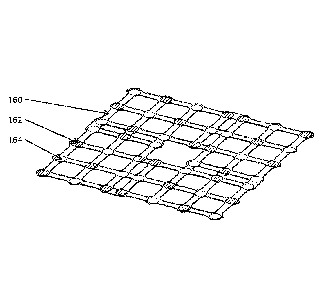
[0025] Figure 2 shows an exemplary spring suitable to facilitate an
engineered compliance
when used to support a semiconductor anode assembly.
[0026] Figure 3 shows the simulated force versus compliance response for
the exemplary
spring of Figure 2.
[0027] Figure 4 shows a highly exaggerated simulated deflection for the
exemplary spring of
Figure 2 when loaded with forces similar to those experienced in the inventive
application. The
base shown in the figure is simply part of the simulation and does not
represent the current
invention. This figure is included to aid the reader to visualize the
functionality of the spring.
[0028] Figure 5 depicts an exemplary insulating spacer brazed or soldered
to an outer comer
of the anode assembly.
[0029] Figure 6 shows a view of a combined vacuum package and anode
assembly. The
view is presented from the direction typically covered by the photocathode.
The view shows an
exemplary embodiment that makes use of 4 insulating spacers.
[0030] Figure 7 shows a view of a combined vacuum package and anode
assembly suitable
for use in an alternate embodiment of the present invention. The view is
presented from the
direction typically covered by the photocathode. The view shows an exemplary
embodiment
that makes use of a single insulating spacer.
[0031] Figure 8 shows a sectioned view of the photocathode assembly.
[0032] Figure 9 shows a close-up of a portion of a vacuum package assembly
joined to an
anode assembly using an alternate multiple spring approach.
6
DETAILED DESCRIPTION
100331 Figure 1
shows a cross-sectional view of an EBAPS image intensifier incorporating
an exemplary embodiment of the invention. The vacuum package assembly (110) is
typically
based on a hermetic, multi-layer, high temperature co-fired ceramic package
fabricated via
conventional means. As shown in Figure 1, the ceramic package employs a
ceramic design
protected under the claims of US Patent 6,837,766. As detailed in US patent
6,837,766 B2, the
non-monotonically varying inner ceramic side wall of the vacuum package
increases the high
voltage stand-off potential of the wall and therefore improves sensor yield.
The vacuum
package (110) assembly is sealed to a photocathode assembly (120) by means of
a sealing
material (150) in order to complete a vacuum envelope. The vacuum envelope
encloses an
anode assembly (130). The photo-emissive portion of the photocathode assembly
resides on the
inner surface of the assembly (122) facing the electron sensitive portion of
the anode assembly
(132). The photo-emissive portion of the photocathode (122) is typically
planar. Light enters
the sensor through the photocathode assembly (120) about an optical axis (10)
that is essentially
perpendicular to the planar photo-emissive surface (122). Detected light is
absorbed at the
photo-emissive surface (122) resulting in a significant probability of
photoelectron emission.
Photon absorption and photoelectron emission are typically spatially
correlated to within a few
microns for the GaAs photocathode used in the exemplary embodiment. The basic
physics of
the GaAs Photocathode is described in publication: Applied Physics 12, 115-130
(1977) by
William E Spicer: Negative Affinity 3-5 Photocathodes: Their Physics and
Technology. The
electron sensitive surface of the anode assembly may be optionally overlaid
with a collimator as
detailed in US Patent 8,698,925. This facing arrangement of the photocathode
and anode
assembly is typical of proximity focused image intensifiers. In US patent
6,998,635 B2 Sillmon
gives a detailed description of a GaAs/AlGaAs photocathode assembly using an
advanced filter
structure. A preferred embodiment of the invention incorporates a GaAs/AlGaAs
photocathode
assembly similar to that described by Sillmon. It should be noted that the
filter structure,
although it may add advantage to certain system level applications, is not
material to the present
invention. US patent 6,998,635 provides a background on suitable photocathode
assemblies.
Other photocathode assembly types and variations may be incorporated without
violating the
teachings of this disclosure. Specifically, the photocathode assembly may
incorporate a
Transferred Electron photocathode similar to that described in US Patent
5,047,821.
Additionally, a semitransparent alkali photocathode such as that described in
patent application
W02014056550 would be applicable to the teachings of this invention. The
sealing material
(150) may be indium or an alloy of indium as described in US Patent 4,178,528
as
7
Date Recue/Date Received 2023-01-09
CA 02992730 2018-01-16
WO 2017/015028 PCT/US2016/042112
described by Kennedy. Other sealing methods to include braze seals, solder
seals or other direct
metal to metal seals may also be used without violating the teachings of this
disclosure. The
anode assembly (130) is physically supported by and joined to the vacuum
package assembly
via one or more springs (160) to facilitate a controlled compliance versus
force response as the
anode assemble is pushed into the internal cavity of the vacuum package as
seen in the cross
section if Figure 1. This provides a flexible attachment of the anode to the
packaging. In this
exemplary embodiment, the spring is brazed or soldered to both the anode
assembly (130) and
the vacuum package assembly (110). The braze or solder material (170) may be
chosen from a
wide variety of materials familiar to those skilled in the art of ultra-high
vacuum (UHV) die
attach. Suitable materials for the braze/solder attach material (170) include
indium, indium
alloys, and a wide variety of commercially available metal alloys which
include "active" braze
materials containing titanium or other reactive metals. Use of an active braze
material can
negate the need for metallized pads on to package or on the back surface of
the anode assembly.
It should be noted that the physical height of the braze material (170) is
engineered such that the
spring (160) can deflect a sufficient distance without contacting the package
or alternately
contacting the back surface of the anode assembly when the photocathode
assembly to package
assembly vacuum seal is generated. Also as shown in Figure 1, in the exemplary
embodiment,
the points of attachment between the spring (160) and the anode assembly (130)
are spatially
staggered with the points of attachment between the spring (160) and the
vacuum package
assembly (110). This configuration is essentially a modified leaf spring. In
the exemplary
embodiment, a preferred braze or solder material (170) will be slightly
malleable using a
malleable bonding agent. This malleability limits the peak stress in the
spring (160) at the edge
of the contact area between the materials. Indium is a preferred braze /
solder material (170).
Electrical connections from the anode assembly to the inner surface of the
vacuum package
either via wire bonds (180), through the braze / solder (170) and spring (160)
or both paths.
Multiple electrically isolated springs may be arrayed below the anode assembly
to provide
multiple isolated electrical paths to the anode assembly to support signal and
power connections.
Similarly, metallized traces on an insulating spring substrate may be used in
conjunction with
vias to make use of the spring as an electrical redistribution layer. However,
wirebonds
typically offer the most cost effective and reliable approach to deal with the
high lead counts
common on high performance CMOS based anode assemblies. Figure 1 also depicts
insulating
spacers (140) which are attached to the anode assembly via bonding material
(190). Materials
that can be used for insulating spacer (140) include but are not limited to
glass, quartz, sapphire,
alumina, mullite, SiNX,A1NX, All\Tx0y and a wide variety of other minerals and
ceramics. The
bonding material (190) can likewise be a braze or solder including In, InSn,
InAg, InCu, InPb,
8
CA 02992730 2018-01-16
WO 2017/015028 PCT/US2016/042112
SnPb, InPbAg, AuSn, AuGe, AuSi, AlGe, combinations of the previously listed
materials or a
wide variety of other commercially available bonding materials. The contact,
shown in Figure
1, between the insulating spacer (140), of the anode assembly, and the
photocathode assembly
(120) results from the force created by the deflection of the spring (160)
during the vacuum
sealing process.
[0034] Figure 8 is a cross-sectioned sketch of photocathode assembly (120)
that shows
additional features that are not visible in Figure 1. Incoming light travels
through photocathode
assembly (120) and is at least partially absorbed by the photo-emissive
material located in the
area depicted as 122 on the surface of the photocathode assembly. In the
exemplary
embodiment depicted in Figure 8 the exposed photo-emissive surface consists of
P-Type GaAs.
Numerous other photo-emissive surfaces may be used without violating the
teachings of this
invention. 124 indicates a contact area that is nominally co-planar to the
photo-emissive
surface. 126 indicates a conductive surface coating a trough that separates
the plateau consisting
of surface 122 combined with 124 and a vacuum seal surface consisting of
combined surfaces
128 and 129. The area indicated by 128 is coated with a conductive layer.
Section 129 is
nominally coplanar with section 128 but is not coated with a conductive layer.
Section 129 may
be a bare glass surface. For the exemplary embodiment depicted in Figure 8,
Corning Code
7056 glass is demonstrated to be an appropriate material. The conductive layer
extending over
the surfaces depicted by 124, 126 and 128 is a continuous layer. The layer is
typically a metal.
Numerous metals may provide an acceptable contact layer. Potential candidate
metals include
but are not limited to Cr, Co, Ag, Au, Pt, Ir, Ni, Ti, Ta, W, V, Zr, Fe, Al,
Cu, C, Si and alloys of
the previously listed materials. The layer must have sufficient conductivity
to replenish the
photoelectrons emitted from photo-emissive surface 122. Typical contact layer
thicknesses are
on the order of 0.05 to 2 microns. Consequently, photo-emissive surface 122 is
essentially co-
planar with contact layer 124. It should be noted that spacer 140 may overlay
photo-emissive
surface 122, contact layer 124 or a combination of both areas without adverse
consequence.
[0035] Figure 2 depicts an exemplary embodiment of an appropriate spring
(160) that can be
used to support an anode assembly. The spring may be manufactured from a
variety of materials
including ceramics, silicon, oxidized silicon, glass, metallized glass,
nitrided silicon, nickel,
cobalt, metal alloys such as steel, Kovar, beryllium copper, Ni-Co and Fe-Co.
A selection of
materials not specifically called out in the list above may be made based on
favorable
mechanical and thermal properties without violating the teachings of this
disclosure.
Manufacturing methods for the spring can include etching, machining, laser
cutting,
electroforming and additive 3D printing. The spring does not need to be flat
when
uncompressed. In fact, a spring that is formed in the unloaded state can be
designed to make
9
CA 02992730 2018-01-16
WO 2017/015028 PCT/US2016/042112
very efficient use of the volume between the vacuum package assembly and the
anode assembly.
In order to achieve repeatable braze or solder profiles, pre-defined
braze/solder pads are used in
a preferred embodiment. The braze pads visible on the exposed surface (162) of
Figure 2 are
depicted by cross-hatched circles. The projection of the braze pads present on
the hidden face of
Figure 2 are depicted by the open circles (164). The layout and thickness of
the spring was
based on the mechanical properties of the chosen material. The exemplary
layout used an
electroformed Cobalt-Nickel alloy, with a 50 micron thickness. Computer
modeling of the
spring design depicted in Figure 2 demonstrated that it exhibited sufficient
thermal conductivity
for the power dissipation of the CMOS device used in the anode assembly.
Additionally,
computer modeling showed that the chosen design would achieve the compliance
performance
shown in Figure 3 without experiencing peak stresses that exceed the
material's limits. It is a
goal of the sensor design to minimize movement of the anode assembly (130)
with respect to
both the vacuum package assembly (110) and the photocathode assembly (120) as
the sensor is
exposed to environmental shocks and vibration. The total effective "sprung
mass" for the anode
assembly was calculated and compared to the forces generated by the
anticipated peak
acceleration environmental exposure for the sensor. As the sensor is
accelerated parallel to the
optical axis (10), the vector product of the mass and the acceleration will
sum with the force
applied by the spring (160) and transmitted through the anode assembly (130)
to the spacers
(140). If the forces associated with acceleration of the sensor fully
compensate the force applied
by the spring (160), movement may occur between the anode assembly (130) and
the balance of
the sensor. This analysis, including an engineering margin of safety, was used
to specify the
minimum force required from the spring. The maximum force that was chosen for
this
exemplary embodiment was chosen to be equal to the sea-level atmospheric force
pressing the
photocathode assembly in to the vacuum package assembly. This is a somewhat
arbitrary upper
force limit but it was chosen as a conservative limit. With both force and
deflection goals
established, the geometry and thickness of the spring layout was iterated
until the deflection
versus force profile depicted in Figure 3 was obtained. The minimization of
movement between
the anode assembly (130) and the balance of the vacuum sensor under the
influence of
accelerations on an axis perpendicular to the optical axis (10) is insured by
multiple means.
First, the design of the spring (160) is very resistant to deflection in the
plane perpendicular to
the optical axis. The exemplary spring shown in Figure 2 was modeled and
predicted to deflect
less than one micron for the maximal anticipated acceleration perpendicular to
the optical axis.
Additionally, the force generated by the spring (160) results in a compressive
load between the
inner surface of the photocathode assembly (120) and the surface of spacer
(140). The
coefficient of friction between the spacer (140) and the photocathode assembly
(120) surface
CA 02992730 2018-01-16
WO 2017/015028 PCT/US2016/042112
resists shearing between the two surfaces. This configuration has been shown
to pass required
shock and vibration environmental exposures without visible degradation.
Whereas the
described embodiment is highly resistant to movement between anode assembly
(130) and the
balance of the sensor in high acceleration environments it will accommodate
relative movements
of the components associated with temperature cycling and miss-matched
coefficients of thermal
expansion.
[0036] Figure 4 shows a sketch of modeled deflection of spring (160) on a
test stand with
highly exaggerated deflection, it is meant as a guide to illustrate method of
function of the spring
in the exemplary embodiment. Whereas this geometry meets the thermal and
mechanical
requirements of the exemplary invention, it will be clear to one skilled in
the art that numerous
alternate acceptable spring designs may be created without violating the
teachings of this
disclosure.
[0037] Figure 5 shows a close-up view of an insulating spacer 140
positioned at a comer of
an anode assembly 130. In this view the photocathode assembly is not present
so that the detail
of the anode assembly can be better visualized. The projection of the electron
sensitive imaging
area of the anode assembly is depicted by the surface labeled as 132.
Insulating spacer 140 is
sized and placed so as to not overlap area 132. In this exemplary embodiment,
the anode
assembly includes a collimator as indicated by 134. Although, not visible in
the view of Figure
5, the insulating spacer 140 is soldered or brazed to the collimator, as
depicted in Figure 1. The
collimator is in turn either formed monolithically from the silicon of the
back-thinned CMOS
sensor as described in US Patent 7,479,686 or bonded to the anode surface as
described in US
Patents 7,479,686 or 8,698,925. Wire bond pads are depicted in Figure 5 and
labeled 136. Bond
wires (180) that electrically connect anode assembly pads 136 to wire bond
pads on the internal
surface of the vacuum package assembly (138 Figure 6) are typically routed to
have a very low
rise above the surface of the bond pads (136). This minimizes the electric
field strength above
the bond wares and thereby minimizes the chance that field emission from
particles or sharp
features on the inner surface of the photocathode assembly (120 Figure 1) will
damage the
sensor. In practice, the bond wire height is typically below that of the
bottom surface of the
insulating spacer 140.
[0038] Figure 6 shows a perspective view of the vacuum package assembly
combined with
an anode assembly. In this exemplary embodiment, 4 insulating spacers 140 are
used. As
shown, the placement of the spacers need not be symmetrical. However, the
force generated by
the spring must be engineered such that the compliant anode assembly will
index off of the
photocathode assembly and lay flat against the planar photocathode assembly
surface upon
completion of the photocathode to vacuum package assembly joining process. A
wide variety of
11
CA 02992730 2018-01-16
WO 2017/015028 PCT/US2016/042112
braze or solder materials may be used as the bonding material 190 to join the
insulating spacers
140 to the underlying anode assembly 130. Low vapor pressure, low melting-
point brazes or
solder alloys are preferred at this location due to the limited thermal budget
associated with a
typical CMOS anode assembly. Choice of insulating spacer geometry, material,
anticipated
thermal processing and spacer count may influence the choice of bonding
material 190.
Typically a minimum of three spacers (140), or three attachment placements of
bonding material
(190) to a single spacer are required to robustly specify the relative plane
of the anode assembly
with respect to the plane of the photocathode assembly (120). The use of a
malleable braze
material such as is typical of Indium and certain indium alloys for bonding
material 190 holds a
practical advantage in that a moderate lack of planarity between spacer (140)
and the
photocathode assembly surface (122 or 124) can be accommodated during the
photocathode
assembly (120) to vacuum package assembly (110) joining process via
deformation of bonding
material (190).
[0039] The relative spacing of the bond wires 180 and the spacer 140 allows
the spacer to be
positioned over the bond wires without interference. In an alternate
embodiment of the
invention, the 4-insulating-spacer configuration shown in Figure 6 is replaced
by a single
insulating spacer in Figure 7. The spacer of Figure 7 is made as a single pad
having a cutout
matching the size of the electron sensitive surface of the anode. As
illustrated in Figure 7 the
spacer can overlap the bondwires. It will be clear to one skilled in the art
that a wide variety of
spacer configurations and geometries can be implemented when careful
consideration is given to
materials, thermal coefficients of expansion and anticipated acceleration
loads.
[0040] Figure 9 shows an alternate embodiment of a combined vacuum package
assembly
and anode assembly suitable for use in the current invention. In the exemplary
embodiment
shown in Figure 9 a number of potential modifications to the previously shown
preferred
embodiment are illustrated. First, the monolithic compliant spring 160 shown
in Figure's 1, 2
and 4 has been replaced with multiple spring elements 161. Second, bond wires,
180, have been
functionally replaced by the individual, electrically independent spring
elements. In Figure 9,
spring elements 161 are affixed to vacuum package bond pads 138. The spring
elements
additionally contact and are affixed to bond pads present on the back of anode
assembly 130.
The springs may be affixed to the pads by various means including but not
limited to thermo-
compression bonding, solder and brazing. Bond pads on the back of the anode
assembly may be
generated by a number of methods known to those skilled in the art without
impacting the scope
of teaching in this disclosure. Potential methods to generate backside bond
pads include the use
of through-silicon vias and wrap around metallizations as described in US
Patent 7,607,560 B2.
12
CA 02992730 2018-01-16
WO 2017/015028
PCT/US2016/042112
[0041] It should be understood that processes and techniques described
herein are not
inherently related to any particular apparatus and may be implemented by any
suitable
combination of components. Further, various types of general purpose devices
may be used in
accordance with the teachings described herein. It may also prove advantageous
to construct
specialized apparatus to perform the method steps described herein.
[0042] The present invention has been described in relation to particular
examples, which
are intended in all respects to be illustrative rather than restrictive. Those
skilled in the art will
appreciate that many different combinations of hardware, software, and
firmware will be
suitable for practicing the present invention. Moreover, other implementations
of the invention
will be apparent to those skilled in the art from consideration of the
specification and practice of
the invention disclosed herein. It is intended that the specification and
examples be considered
as exemplary only, with a true scope and spirit of the invention being
indicated by the following
claims.
13