Note : Les descriptions sont présentées dans la langue officielle dans laquelle elles ont été soumises.
CA 02992855 2018-01-17
WO 2017/039962
PCT/US2016/045998
1
INTEGRATION OF INDUCTORS WITH ADVANCED-NODE
SYSTEM-ON-CHIP (SOC) USING GLASS WAFER WITH
INDUCTORS AND WAFER-TO-WAFER JOINING
Field of Disclosure
[0001] Various embodiments described herein relate to integrated
circuit devices, and
more particularly, to integrated circuit devices with voltage regulators.
Background
[0002] Voltage regulators have been implemented in conventional
dedicated power
management integrated circuits (PMICs). A conventional PMIC, which is separate
from other integrated circuits on a circuit board, may have difficulty meeting
the droop
(transient) and power (efficiency) requirements of a modern multi-core
application
processor or communication processor, for example.
[0003] There
has been a growing interest in integrating voltage regulators as part of
system-on-chip (SOC) integrated circuit devices.
Integrated voltage regulators,
however, may present several challenges in chip design and layout. For
example,
passive components such as inductors and capacitors in voltage regulators may
pose a
design challenge, because passive components, such as inductors and
capacitors,
especially those with large inductance and capacitance values, typically have
large form
factors requiring large surface areas in a typical layout for a silicon SOC
die.
[0004] Moreover, inductors in voltage regulators typically require very
low resistances
to minimize power losses in voltage regulation. In addition to occupying a
significant
amount of surface area of a typical silicon SOC die, such inductors may
require thick
metal traces on the SOC die in order to reduce the resistance values of the
inductors. In
advanced-node SOC wafer fabrication, however, such thick metal traces may not
be
feasible. Moreover, even if thick metal traces are implementable on a silicon
SOC die,
conventional fabrication processes for integrating inductors as part of a
voltage
regulator on a silicon SOC die may require several additional masks, thereby
increasing
the cost of fabrication.
CA 02992855 2018-01-17
WO 2017/039962
PCT/US2016/045998
2
SUMMARY
[0005] Exemplary embodiments of the disclosure are directed to
integrated circuit
devices and methods of making the same. In an embodiment, a voltage regulator
is
integrated or embedded in a system-on-chip (SOC) device which also includes
one or
more circuits using the voltage supplied by the voltage regulator.
[0006] In an embodiment, a device is provided, the device comprising: a
system-on-
chip (SOC) wafer; an inductor wafer having first and second surfaces and a
plurality of
vias therethrough, the vias forming a plurality of sidewalls in the inductor
wafer,
wherein the first surface of the inductor wafer is disposed adjacent to the
SOC wafer; a
magnetic layer on at least a portion of the first surface of the inductor
wafer; and a
conductive layer disposed on the magnetic layer, on at least a portion of the
second
surface of the inductor wafer, and on at least some of the sidewalls formed by
the vias in
the inductor wafer.
[0007] In another embodiment, a device is provided, the device
comprising: a voltage
regulator, comprising: a die; an inductor wafer having first and second
surfaces and a
plurality of vias therethrough, the vias forming a plurality of sidewalls in
the inductor
wafer, wherein the first surface of the inductor wafer is disposed adjacent to
the die; a
magnetic layer on at least a portion of the first surface of the inductor
wafer; and a
plurality of conductors disposed within at least some of the vias in the
inductor wafer,
the conductors having respective first ends adjacent to the first surface of
the inductor
wafer and second ends adjacent to the second surface of the inductor wafer;
and a
system-on-chip (SOC) package configured to receive a power supply voltage from
the
voltage regulator, the SOC package having at least one conductor connected to
at least
one of the first and second ends of the conductors.
[0008] In another embodiment, a method of making a device is provided,
the method
comprising: providing a first wafer having a first surface and a second
surface; forming
a plurality of vias through the first and second surfaces of the first wafer,
wherein the
vias are defined by a plurality of sidewalls within the first wafer; forming a
patterned
magnetic layer on at least a portion of the first surface of the first wafer;
forming a
conductive layer on the patterned magnetic layer over the patterned magnetic
layer, at
least a portion of the second surface of the first wafer, and at least some of
the sidewalls
of the vias; and joining a second wafer to the first wafer.
CA 02992855 2018-01-17
WO 2017/039962
PCT/US2016/045998
3
[0009] In yet another embodiment, a method of making a device is provided,
the
method comprising: providing a system-on-chip (SOC) package; and forming a
voltage
regulator on the SOC package, comprising: providing an SOC die; providing an
inductor wafer having first and second surfaces, wherein the first surface of
the inductor
wafer is disposed adjacent to the SOC die; forming a plurality of vias through
the first
and second surfaces of the inductor wafer, wherein the vias are defined by a
plurality of
sidewalls in the inductor wafer; and forming a plurality of conductors
disposed within at
least some of the vias in the inductor wafer, the conductors having respective
first ends
adjacent to the first surface of the inductor wafer and second ends adjacent
to the second
surface of the inductor wafer, wherein the SOC package is configured to
receive a
power supply voltage from the voltage regulator, the SOC package having at
least one
conductor connected to at least one of the first and second ends of the
conductors.
BRIEF DESCRIPTION OF THE DRAWINGS
[0010] The accompanying drawings are presented to aid in the description of
embodiments of the disclosure and are provided solely for illustration of the
embodiments and not limitation thereof
[0011] FIG. 1 is a perspective view illustrating an embodiment of a system-
on-chip
(SOC) wafer.
[0012] FIG. 2 is a perspective view illustrating an embodiment of an
inductor wafer
with through vias.
[0013] FIG. 3 is a perspective view illustrating an embodiment of face-to-
face wafer-to-
wafer bonding of an SOC wafer and an inductor wafer.
[0014] FIG. 4 is a sectional view illustrating an embodiment of a first
process step in
the manufacturing of an inductor on an inductor wafer with through vias.
[0015] FIG. 5 is a sectional view illustrating an embodiment of a second
process step in
the manufacturing of the inductor with a patterned thin-film magnetic layer.
[0016] FIG. 6 is a sectional view of an embodiment of a third process step
in the
manufacturing of the inductor with a dielectric on the thin-film magnetic
layer.
[0017] FIG. 7 is a sectional view of an embodiment of a fourth process step
in the
manufacturing of the inductor with metal plating.
[0018] FIG. 8 is a top plan view of an inductor having a coil with multiple
loops.
CA 02992855 2018-01-17
WO 2017/039962
PCT/US2016/045998
4
[0019] FIG. 9
is a sectional view illustrating an embodiment of a fifth process step in
the manufacturing of a system-on-chip (SOC) device by joining an SOC wafer
with an
inductor wafer.
[0020] FIG. 10 is a sectional view illustrating an embodiment of the
SOC device of
FIG. 9 after the SOC wafer and the inductor wafer are joined together.
[0021] FIG. 11 is a perspective view illustrating an embodiment of an
inductor die after
dicing of the joined SOC wafer and inductor wafer.
[0022] FIG. 12 is a sectional view illustrating an embodiment of a
system including a
printed circuit board (PCB), an SOC package, and a voltage regulator which
includes an
inductor die.
[0023] FIG. 13 is a diagram illustrating am embodiment of a system
including a power
management integrated circuit (PMIC) and an SOC device which includes an
integrated
or embedded voltage regulator and circuit using the voltage regulator.
DETAILED DESCRIPTION
[0024] Aspects of the disclosure are described in the following
description and related
drawings directed to specific embodiments. Alternate embodiments may be
devised
without departing from the scope of the disclosure. Additionally, well-known
elements
will not be described in detail or will be omitted so as not to obscure the
relevant details
of the disclosure.
[0025] The word "exemplary" is used herein to mean "serving as an
example, instance,
or illustration." Any embodiment described herein as "exemplary" is not
necessarily to
be construed as preferred or advantageous over other embodiments. Likewise,
the term
"embodiments" does not require that all embodiments include the discussed
feature,
advantage or mode of operation.
[0026] The terminology used herein is for the purpose of describing
particular
embodiments only and is not intended to be limiting of the embodiments. As
used
herein, the singular forms "a," "an" and "the" are intended to include the
plural forms as
well, unless the context clearly indicates otherwise. It will be further
understood that
the terms "comprises," "comprising," "includes" or "including," when used
herein,
specify the presence of stated features, integers, steps, operations,
elements, and/or
components, but do not preclude the presence or addition of one or more other
features,
CA 02992855 2018-01-17
WO 2017/039962
PCT/US2016/045998
integers, steps, operations, elements, components, or groups thereof Moreover,
it is
understood that the word "or" has the same meaning as the Boolean operator
"OR," that
is, it encompasses the possibilities of "either" and "both" and is not limited
to
"exclusive or" ("XOR"), unless expressly stated otherwise. It is also
understood that
the symbol "/" between two adjacent words has the same meaning as "or" unless
expressly stated otherwise. Moreover, phrases such as "connected to," "coupled
to" or
"in communication with" are not limited to direct connections unless expressly
stated
otherwise.
[0027] FIG. 1 is a perspective view illustrating an embodiment of a
system-on-chip
(SOC) wafer 100 having a first surface 102 and a second surface 104 opposite
each
other. In an embodiment, the SOC wafer 100 comprises a semiconductor wafer,
such as
a silicon wafer. In alternate embodiments, the SOC wafer 100 may comprise a
glass
wafer, a quartz wafer, an organic wafer, or a wafer made of another material.
In an
embodiment, the SOC wafer 100 may be integrated with an inductor wafer on
which
one or more inductors are provided.
[0028] FIG. 2 is a perspective view illustrating an embodiment of an
inductor wafer 200
with a plurality of through vias 202a, 202b, 202c, .... In the embodiment
illustrated in
FIG. 2, the inductor wafer 200 has first and second surfaces 204 and 206
opposite each
other, and the vias 202a, 202b, 202c, ... are formed through the first and
second
surfaces 204 and 206 of the inductor wafer 200. In an embodiment, the inductor
wafer
200 comprises a glass wafer. In alternate embodiments, the inductor wafer 200
may
comprise a quartz wafer, an organic wafer, or another type of low-loss
dielectric
material, to ensure that the inductor fabricated on the inductor wafer 200 has
a low
parasitic loss. For simplicity of illustration, detailed structure of the
conductors in the
vias 202a, 202b, 202c, ... and the patterned conductive layers on the first
and second
surfaces 204 and 206 of the inductor wafer 200 which form one or more coils of
an
integrated inductor are not shown in the perspective view of FIG. 2.
Embodiments of
the integrated inductor formed on the inductor wafer 200 will be described in
further
detail below with respect to FIGs. 4-7 and the top plan view of FIG. 8.
[0029] FIG. 3 is a perspective view illustrating an embodiment of face-
to-face wafer-to-
wafer bonding of the SOC wafer 100 and the inductor wafer 200. In this
embodiment,
the second surface 104 of the SOC wafer 100 is joined with the first surface
204 of the
CA 02992855 2018-01-17
WO 2017/039962
PCT/US2016/045998
6
inductor wafer 200. Again, detailed structure of the integrated inductor
formed on the
inductor wafer 200 is omitted in FIG. 3 for simplicity of illustration.
Embodiments of
the integrated inductor formed on the inductor wafer 200 will be described
with respect
to FIGs. 4-8.
[0030] FIG. 4 is a sectional view illustrating an embodiment of a first
process step in
the manufacturing of an inductor on an inductor wafer with through vias. In
FIG. 4, an
inductor wafer 400 having a first surface 402 and a second surface 404 is
provided. The
inductor wafer 400 may be a glass wafer, a quartz wafer, or another type of
wafer made
of a low-loss dielectric material, for example. In the embodiment shown in
FIG. 4, first
and second vias 406 and 408 are formed within the inductor wafer 400 through
the first
and second surfaces 402 and 404.
[0031] FIG. 5 is a sectional view illustrating an embodiment of a
second process step in
the manufacturing of the inductor with a magnetic layer. In FIG. 5, a magnetic
layer,
such as a patterned thin-film magnetic layer 410, is formed on the first
surface 402 of
the inductor wafer 400. In the embodiment illustrated in FIG. 5, the patterned
thin-film
magnetic layer 410 is formed on the first surface 402 of the portion of the
inductor
wafer 400 between the first and second vias 406 and 408.
[0032] The patterned thin-film magnetic layer 410 may be fabricated in
various
manners. For example, a magnetic material, such as cobalt-tantalum-zirconium
(CoTaZr), may be deposited by vacuum processes, plated, screen-printed, or
laminated
onto the first surface 402 of the inductor wafer 400 to form the thin-film
magnetic layer
410. Other magnetic materials, such as alloys of nickel-iron (NiFe), cobalt-
iron (CoFe),
or cobalt-nickel-iron (CoNiFe), with added materials such as phosphorus (P),
boron (B)
or carbon (C), may be used for the patterned thin-film magnetic layer 410 to
tailor the
magnetic and electrical properties of the patterned thin-film magnetic layer
410. In an
embodiment, the magnetic material for the patterned thin-film magnetic layer
410 is
chosen so as to enable a boost in the inductance value of the inductor at the
appropriate
operating frequencies. Other types of magnetic materials may also be
implemented as
the patterned thin-film magnetic layer 410. The magnetic layer 410 may also be
formed
by other techniques, for example, by sputtering a magnetic material on the
first surface
402 of the inductor wafer 400.
CA 02992855 2018-01-17
WO 2017/039962
PCT/US2016/045998
7
[0033] FIG. 6
is a sectional view of an embodiment of a third process step in the
manufacturing of the inductor with a dielectric on the patterned thin-film
magnetic
layer. In FIG. 6, a dielectric layer 412 is formed on top of the patterned
thin-film
magnetic layer 410. In the embodiment illustrated in FIG. 6, the dielectric
layer 412
covers the entire top and side surfaces of the thin-film magnetic layer 410,
as well as
portions of the first surface 402 of the inductor wafer 400 surrounding the
patterned
thin-film magnetic layer 410. In an embodiment, the dielectric layer 412
comprises a
polymer dielectric material. In an alternate embodiment, the dielectric layer
412
comprises an inorganic dielectric material, for example, silicon dioxide
(Si02). Other
types of dielectric materials may also be used for the dielectric layer 412
within the
scope of the disclosure.
[0034] FIG. 7 is a sectional view of an embodiment of a fourth process
step in the
manufacturing of the inductor with metal plating. In the sectional view shown
in FIG.
7, the first via 406 has sidewalls 414 and 416, and likewise, the second via
408 has
sidewalls 418 and 420 between the first and second surfaces 402 and 404 of the
inductor
wafer 400. In an embodiment, a conductive layer 422 is formed on the
dielectric layer
412, on the sidewall 416 of the first via 406, on the sidewall 418 of the
second via 408,
and on the second surface 404 of the inductor wafer 400 between the first and
second
vias 406 and 408. In an embodiment, the conductive layer 422 is formed by
metal
plating.
[0035] In a further embodiment, the conductive layer is formed by semi-
additive plating
of a metal such as copper (Cu). In the sectional view shown in FIG. 7, the
sidewall 414
opposite the sidewall 416 the first via 406 and at least portions of the first
and second
surfaces 402 and 404 of the inductor wafer 400 adjacent to the sidewall 414
are also
covered by a conductive layer 424. Likewise, as shown in FIG. 7, the sidewall
420
opposite the sidewall 418 the second via 408 and at least portions of the
first and second
surfaces 402 and 404 of the inductor wafer 400 adjacent to the sidewall 420
are also
covered by a conductive layer 426. Similar to the conductive layer 422, the
conductive
layers 424 and 426 may also be formed by metal plating, such as semi-additive
copper
plating.
[0036] In the embodiment illustrated in the sectional view of FIG. 7,
the conductive
layer 422 is shown as a section of one loop of an inductor coil which
comprises a
CA 02992855 2018-01-17
WO 2017/039962
PCT/US2016/045998
8
plurality of loops. A top plan view of an embodiment of a solenoid inductor
which
comprises an inductor coil with multiple loops is shown in FIG. 8, which will
be
described in further detail below. Other inductor topologies, for example,
spiral
inductors, toroid inductors, or racetrack inductors, may also be implemented
instead of
the solenoid inductor in the embodiments described and illustrated herein. In
an SOC
package with a limited amount of space, however, a solenoid inductor may be
chosen
for its small footprint and easy, efficient integration closest to the
circuitry on the SOC
die.
[0037] Referring to the embodiment shown in FIG. 7, the conductive
layer 422, which
is illustrated as the sectional view of one loop of coil of an inductor,
surrounds the thin-
film magnetic layer 410, which is implemented as a magnetic core of the
inductor. In
an alternate embodiment, another magnetic layer may be provided within the
inductor
coil, for example, a magnetic layer formed on the second surface 404 of the
inductor
wafer 400 opposite the magnetic layer 410 as shown in FIG. 7, to increase the
overall
magnetic flux and thus the overall inductance of the inductor. In another
alternate
embodiment, an inductor with multiple loops of coil, with each loop having a
sectional
view similar to the sectional view of the conductive layer 422 as shown in
FIG. 7, may
be provided without any magnetic layer inside the coil, although such an
inductor with
no magnetic core would have a lower inductance compared to an inductor of the
same
size and the same number of loops having one or more magnetic cores.
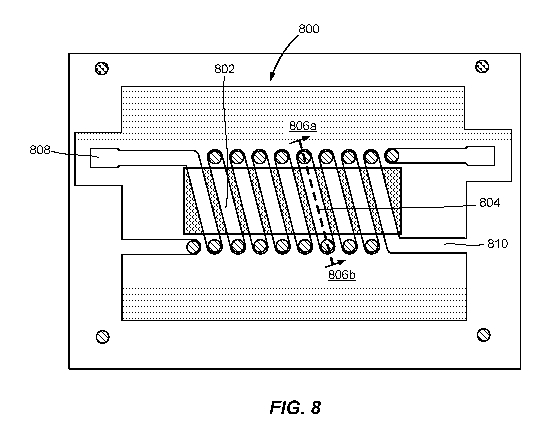
[0038] FIG. 8 is a top plan view of an inductor 800 having a coil 802
with multiple
loops before the SOC wafer is joined with the inductor wafer. In an
embodiment, a
sectional view of one of the loops 804 taken along sectional line 806a-806b is
illustrated
in FIG. 7. Referring to the top plan view of FIG. 8, the inductor 800 has two
terminals
808 and 810 at two opposite ends of the coil 802 for electrical connections
with other
circuit components in a voltage regulator, for example. In an embodiment, some
of the
pass-through vias in the inductor wafer 400, like the first via 406 and the
second via 408
as illustrated in FIGs. 4-7, may be used to form electrical connections
between die pads
on the SOC die and pads on the substrate. For example, some of the pass-
through vias
may be connected to enable power supply connections and/or to provide ground
planes
to improve power delivery to the SOC die. In an embodiment, the conductive
layer 422,
which may comprise a thick Cu plating on the inductor wafer 200, can be used
as an
CA 02992855 2018-01-17
WO 2017/039962
PCT/US2016/045998
9
additional routing layer to improve the performance of an advanced node SOC
device
with an advanced node SO C wafer 100. In a further embodiment, by using a
combined
design of the advanced node SO C wafer 100, the inductor wafer 200, and a
package
substrate 1212 on an integrated circuit (IC) package 1204, which will be
described in
further detail below with respect to FIG. 12, the thick Cu plating of the
conductive layer
422 can be used to reduce the number of Cu layers in the advanced node SO C
wafer
100, or in the package substrate 1212, or both.
[0039] FIG. 9 is a sectional view illustrating an embodiment of a fifth
process step in
the manufacturing of a system-on-chip (SOC) device by joining an SO C wafer
with an
inductor wafer. In an embodiment, the SO C wafer 100 is provided with a
plurality of
metal columns, such as metal column 902 on the second surface 104 of the SO C
wafer.
In an embodiment, a solder 904 is provided on the metal column 902 for joining
with a
respective metal-plated via of the inductor wafer. In the sectional view
illustrated in
FIG. 9, the metal column 902 on the second surface 104 of the SO C wafer 100
is
aligned with the via 408 in the inductor wafer 400, which is described above
with
respect to FIG. 7. For simplicity of illustration, the thin-film magnetic
layer 410 and the
dielectric layer 412 are omitted in the sectional view of FIG. 9.
[0040] FIG. 10 is a sectional view illustrating an embodiment of the SO
C device of
FIG. 9 after the SO C wafer and the inductor wafer are joined together. In the
embodiment illustrated in FIG. 10, the solder 904 connects the top portions of
conductors 422 and 426 over the sidewalls 418 and 420 of the via 408,
respectively, and
is positioned directly over the via 408 in the inductor wafer 400. In an
embodiment, the
solder 904 may comprise a conventional solder material that melts under heat
and
solidifies when the temperature cools down.
[0041] FIG. 11 is a perspective view illustrating an embodiment of an
inductor die after
dicing of the joined SO C wafer and inductor wafer. In typical wafer
fabrication
processes, multiple identical chips may be fabricated on a single wafer with a
large
surface area. In an embodiment, a chip may be separated from a wafer by one of
many
dicing techniques known to persons skilled in the art. In the embodiment shown
in FIG.
11, the joined SO C wafer 100 and the inductor wafer 200 may be diced into a
plurality
of dies 1102a, 1102b, 1102c, .... Any one of the dies 1102a, 1102b, 1102c, ...
may
CA 02992855 2018-01-17
WO 2017/039962
PCT/US2016/045998
include one or more inductors and one or more other components, such as one or
more
capacitors, as part of an integrated or embedded voltage regulator.
[0042] FIG. 12 is a sectional view illustrating an embodiment of a
system including a
printed circuit board (PCB), an SOC package, and a voltage regulator which
includes an
inductor die. In FIG. 12, a printed circuit board (PCB) 1202 is provided, and
an IC
package 1204 is provided on the PCB 1202. In an embodiment, the IC package may
include one or more analog integrated circuits, one or more digital integrated
circuits, or
a combination thereof In an embodiment, the IC package 1204 may have one of
various configurations known to persons skilled in the art, including but not
limited to
wirebond, flip-chip, or ball grid array (BGA), for example.
[0043] Referring to FIG. 12, a die 1206 that includes an inductor
fabricated on an
inductor wafer with through vias and joined with an SOC wafer in embodiments
described above with respect to FIGs. 1-11 is integrated with the IC package
1204. In
an embodiment, the IC package 1204 includes a package substrate 1212. In an
embodiment, the die 1206 may be provided as a part of the circuitry for an
integrated or
embedded voltage regulator 1208, which may also include other components. For
example, the voltage regulator 1208 may include one or more additional passive
components such as one or more capacitors. In FIG. 12, the rest of the
circuitry for the
voltage regulator 1208 are generically indicated by block 1210.
[0044] FIG. 13 is a simplified block diagram illustrating am embodiment
of a system
including a power management integrated circuit (PMIC) and an SOC device which
includes an integrated or embedded voltage regulator and circuit using the
voltage
regulator. In the embodiment illustrated in FIG. 13, the PMIC 1302 is shown as
a chip
separate from the SOC device 1304. In an alternate embodiment, the PMIC 1302
may
be integrated as part of the SOC device 1304. Referring to FIG. 13, the SOC
device
includes an inductor and capacitor (L & C) block 1306, a voltage regulator
(VR) 1308,
and one or more circuits 1310 using the output voltage from the VR 1308. In an
embodiment, the inductor and capacitor in the L & C block 1306 may be
integrated or
embedded with the VR 1308 on the same chip as the circuits 1310 using the
output
voltage from the VR 1308 in an SOC device.
[0045] While the foregoing disclosure shows illustrative embodiments,
it should be
noted that various changes and modifications could be made herein without
departing
CA 02992855 2018-01-17
WO 2017/039962
PCT/US2016/045998
11
from the scope of the appended claims. The functions, steps or actions of the
method
claims in accordance with embodiments described herein need not be performed
in any
particular order unless expressly stated otherwise. Furthermore, although
elements may
be described or claimed in the singular, the plural is contemplated unless
limitation to
the singular is explicitly stated.