Note : Les descriptions sont présentées dans la langue officielle dans laquelle elles ont été soumises.
CA 03003778 2018-04-30
WO 2017/087604 PCT/US2016/062413
INTERFERENCE FILTER FILM FOR DISPLAY APPLICATIONS
Technical Field
[0001] The present application describes an interference filter film for
display
applications, in particular for illuminated screens.
Background
[0002] Several types of displays require high-performance (high
selectivity) light
filtering for various reasons. Regular LED backlit displays (e.g., phones,
tablets, laptops,
TV sets, desktop monitors and other digital displays) have blue LED components
with
radiation that is harmful to eyes, brain and general health. Certain displays
have
emissions above 600 nm that need to be blocked for applications in military,
automotive
industry, etc. Some types of displays with phosphor or other light converting
materials in
their pixels that are excited by blue or UV light need to contain and block
the excessive
excitation light from leaving the screen surface. A selective light filter can
enhance color
contrast in certain display units. Similarly, a selective light filter may
improve display
contrast and visibility in outdoor environments with abundant ambient light.
Another
example is a selective light filter that helps colorblind people to see colors
with higher
contrast and distinction by blocking the portion of the emitted light spectrum
that
confuse brain due to overlapping sensitivity curves of retinal cone and rod
cells.
[0003] High-performance filters that are needed in such cases must be
thin-film
interference filters comprising several sub-wavelength layers. Traditional
methods of
producing high-performance thin-film filters are based on vacuum deposition
methods
1
CA 03003778 2018-04-30
WO 2017/087604 PCT/US2016/062413
such as Ion-Beam Sputtering. These methods are widely used to produce hard-
coated
filters on rigid substrates used in a wide variety of applications and
industries. However,
display industry can hardly use traditional filters for a few reasons: 1)
rigid filters cannot
be simply integrated into the construction of a display cover, 2) existing
thin-film-coated
optical filters are typically on thick glass substrates that can be too bulky
and heavy for
display applications, 3) traditional filter manufacturing processes present
several
technical challenges such as cracking under bending stress that makes them
inappropriate for display integration, and 4) traditional vacuum-deposition-
based
manufacturing is not economically viable for large-volume production of
filters with large
surface areas for display applications.
[0004] 95% of Americans look at LED screens during night time, whether on
computers, laptops, tablets or smart phones. 63% of Americans are not getting
enough
sleep. Similar statistics can be found around the world. Human eyes are
naturally
designed for processing much smaller doses of light at night, especially
certain portions
of the blue light spectrum. A lower intensity of blue light will result in an
increase in our
normal melatonin hormone level. Melatonin will, in turn, make us feel tired
enough to get
a good night's sleep.
[0005] Excessive blue light from LED screens tricks our brain into
thinking
daytime has been prolonged, confusing our internal clock that regulates sleep
and wake
patterns. Screen time at night has shown significant drops in this regulatory
hormone
increasing the risk for depression, stress, insomnia, sleep deprivation, and
in many
cases weight gain, diabetes and certain cancers (breast, ovarian and
prostate).
2
CA 03003778 2018-04-30
WO 2017/087604 PCT/US2016/062413
[0006] People of all ages are affected by blue light. Young teens and
adolescents, however, are more prone to the harmful effects of blue light
because their
eyes work more efficiently causing a higher sensitivity to this particular
light.
[0007] The most harmful part of the blue light that is emitted from most
displays
and causes several health issues is mostly confined to the wavelength range
460 nm to
480 nm. Spectrally, this is an area on the tails of blue LED radiation
spectrum in
displays. Current solutions to this problem include dimming through software
of the blue
LED causing a change in the display color and color temperature. However,
since the
blue LED component, in a vast majority of modern displays, provides excitation
energy
for the green and red LEDs too, it is impossible to turn the blue LED off or
sufficiently
dim it to eliminate the harmful radiation in the range 460 nm ¨ 480 nm.
Summary
[0008] With the advent of all-plastic thin-film interference filters made
through
thermal drawing process, the present application proposes thin-film filter
films for
display applications.
[0009] According to the present disclosure, an optical filter for a
display includes
a filter film with at least one optical filter layer. The filter layer blocks
a band of optical
wavelengths and is transparent for optical wavelengths outside the band. The
filter film
has a thickness within the range of 10 microns through 1 mm. The filter film
may
include one or more laminate layers that are optically transparent in the
wavelengths of
the band blocked by the filter layer. The filter film may include one or more
layers of
liquid crystal polymers in layered contact with one or more transparent
electrode layers
3
CA 03003778 2018-04-30
WO 2017/087604 PCT/US2016/062413
and one or more layers of polymers in layered contact with the one or more
layers of
liquid crystal polymers.
[0010] These and other objects, features and advantages of the subject
matter
herein will become clearer when the drawings as well as the detailed
description are
taken into consideration.
Brief Description of the Drawings
[0011] For a fuller understanding of the nature of the present invention,
reference
should be made to the following detailed description taken in connection with
the
accompanying drawings.
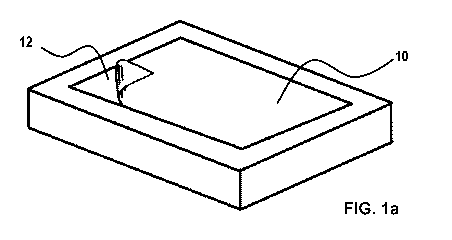
[0012] FIGS. la and lb illustrate an embodiment of a filter film.
[0013] FIGS. 2a and 2b illustrate an embodiment of a filter film with an
adhesive
layer.
[0014] FIG. 3 illustrates an embodiment of a filter film with a secondary
laminate
layer.
[0015] FIG. 4 illustrates an embodiment of a filter film with two
secondary
laminate layers.
[0016] FIG. 5 illustrates an embodiment of a filter film a secondary
laminate layer
and an adhesive applied to one surface.
[0017] FIG. 6 illustrates an embodiment of a filter film with two
secondary
laminate layers and an adhesive applied to one surface.
[0018] FIG. 7 illustrates an embodiment of a filter film in a frame.
4
CA 03003778 2018-04-30
WO 2017/087604 PCT/US2016/062413
[0019] FIG. 8 illustrates an embodiment of a filter film integrated into
a device
case.
[0020] FIG. 9 illustrates a further embodiment of a filter film
integrated into a
device case.
[0021] FIG. 10 illustrates an embodiment of a filter film mounted to a
device with
bands.
[0022] FIG. 11 illustrates an embodiment of a tunable filter film.
[0023] FIG. 12a illustrates a detail view of a tunable filter film in a
first state.
[0024] FIG. 12b illustrates a detail view of the tunable filter film of
Fig. 12a in a
second state.
[0025] FIG. 13 shows a graph illustrating the filtering performance of
certain filter
embodiments.
[0026] FIG. 14 shows a graph illustrating the filtering performance of
certain filter
embodiments.
[0027] Like reference numerals refer to like parts throughout the various
views of
the drawings.
Detailed Description
[0028] The following detailed description is merely exemplary in nature
and is not
intended to limit the described embodiments or the application and uses of the
described embodiments. As used herein, the word "exemplary" or "illustrative"
means
"serving as an example, instance, or illustration." Any implementation
described herein
as "exemplary" or "illustrative" is not necessarily to be construed as
preferred or
CA 03003778 2018-04-30
WO 2017/087604 PCT/US2016/062413
advantageous over other implementations. All of the implementations described
below
are exemplary implementations provided to enable persons skilled in the art to
make or
use the embodiments of the disclosure and are not intended to limit the scope
of the
disclosure, which is defined by the claims. Furthermore, there is no intention
to be
bound by any expressed or implied theory presented in the preceding technical
field,
background, brief summary or the following detailed description. It is also to
be
understood that the specific devices and processes illustrated in the attached
drawings,
and described in the following specification, are simply exemplary embodiments
of the
inventive concepts defined in the appended claims. Hence, specific dimensions
and
other physical characteristics relating to the embodiments disclosed herein
are not to be
considered as limiting, unless the claims expressly state otherwise.
[0029] Aspects of the present disclosure address the need for thin-film
optical
coatings or hybrid filters comprising both thin-film coatings and absorptive
materials.
The embodiments set forth below may employ thermally drawn optical filters to
be used
for any display application, such as, but not limited to, LED displays. All
such
applications, and similar ones, require very selective optical filters that
block certain
portions of the light spectrum without noticeably affecting other parts of the
spectrum
with reflection, absorption and transmission levels that are well controlled
by design.
[0030] In some embodiments, filter films 10 are made of thermo-plastics
and/or
glass materials, though other materials may be appropriate (or developed in
accordance
with known processes or technologies) for certain applications. The filter
films can be
adapted as a direct cover on screens. In some embodiments, the filter film 10
has a
6
CA 03003778 2018-04-30
WO 2017/087604 PCT/US2016/062413
bending flexibility allowing the filter film 10 to be applied bubble-free and
to be peeled
off from a planar surface.
[0031] The filter film 10 can be laminated with or without an additional
adhesive
layer 14 for retaining the filter film on the display surface 12 directly. For
example, the
filter film 10 of FIG. la adheres directly to display surface 12 via static
cling.
Alternatively, as shown in FIGS. 2a and 2b, the filter film 10 may
additionally include an
adhesive layer 14 for attachment on the display surface 12. The adhesive layer
14 is of
a thickness and strength that ensures attachment of the filter film 10 to the
display
surface 12, but that allows residue-free removal of the filter film 10 from
the display
surface 12. The adhesive layer 14 is preferably pressure-activated.
[0032] Alternatively, the filter films may be integrated within the
structure of a
display panel itself, such that external application or adhesion is not
necessary. Various
methodologies are known in the art for laminating multiple layers of polymers
or
polymeric liquid crystal substrates in display panel construction
applications; the present
disclosure is not intended to be limited by any particular display panel
manufacturing
techniques or processes.
[0033] In some embodiments, polymers or glass materials may be utilized
in the
filter films 10 such that passive filtering or certain spectrum(s) of light is
provided
(without need for electrical voltage application).
[0034] In some embodiments that may include removable filter films 10 or
filter
films 10 incorporated in a display screen, the filter films 10 are laminated
with a
secondary laminate layer 16 or sandwiched between a pair of secondary laminate
layers 16 and 18, with or without an added adhesive layer 14 for adhesion to a
display.
7
CA 03003778 2018-04-30
WO 2017/087604 PCT/US2016/062413
For example, FIG. 3 shows an assembly of a filter layer 20 and a first
laminate layer 16.
An intermediate adhesive layer 14 bonds the filter layer 10 to the laminate
layer 16.
The laminate layer 16 may, for example, provide the properties for sufficient
static cling
to the display surface 12. The intermediate adhesive layer may be, without
limitations,
heat-activated, light-activated, or pressure-activated. Unlike the adhesive
layer for
attachment to the display surface 12, the intermediate adhesive layers are
activated in
the manufacturing process, where various techniques can be applied.
[0035] Additionally or alternatively, a second laminate layer 18 may be
provided
on the side of the filter layer 20 that is remote from the display surface 12.
Fig. 4 shows
the second laminate layer 18 in addition to the first laminate layer 16. If
the filter layer
itself includes sufficient static cling properties or if the filter film is
integrated into a
display, the first laminate layer 16 may be unnecessary.
[0036] FIGS. 5 and 6 correspond to FIGS. 3 and 4, except that the filter
film 10
includes an adhesive layer for attaching the filter film 10 to the display
surface 12.
These four illustrations provide only a few of the possible combinations of
laminate
layers with filter layers. It is further possible to include more than one
filter layer within
the same filter film for providing light filtering in different wavelength
ranges.
[0037] These laminated or sandwiched structures can be applied to a
display
surface 10. The laminate layers 16 and 18 can be selected for additional
mechanical
(strength and scratch resistance) or adhesive properties, for further
protection of the
display surface 12, or for further protection of the filter layer 20 itself.
As noted above,
scratch or abrasion resistance characteristics of a particular laminate layer
16 and 18
8
CA 03003778 2018-04-30
WO 2017/087604 PCT/US2016/062413
may prevent damage to the filter film, the display panel, or both, and so may
inform or
influence the type of material selected for a particular layer.
[0038] In further embodiments, as illustrated in FIG. 7, the filter film
10 (with the
filter layer 20 and optionally with additional layers 16 and 18 and adhesive
layers 14
therebetween) can be integrated into a frame 22 for mounting on displays or
devices.
Such filter films 10 can also be integrated into a device case, as
schematically shown in
FIGS. 8 and 9. For example, the filter film (with the additional layers, if
any) can be
integrated into device covers or sleeves such that the device can be placed
inside the
cover or sleeve temporarily and be removed when needed. As shown in FIG. 8, a
device case 24 may include an insertion slot 26 for replacing the filter film
10 with an
identical new one if the filter film 10 is worn, or with a different one for
filtering out
different wavelengths of light. Fig. 9 shows a different device case 28, to
which the filter
film 10 is attached via a hinged connection 30. FIG. 10 shows an example, in
which the
filter film 10 includes a different attachment feature in the form of elastic
bands 32
forming loops placed around the device to place the filter film 10 on the
display surface.
The length of the elastic bands 32 forming the loops depends on the size of
the device.
In the example of Fig. 10, the filter film 10 includes a frame 22 for
attaching the elastic
bands 32. If the filter film itself has sufficient physical integrity, the
elastic bands may be
attached to the filter film 10 itself without using the frame 22.
[0039] The mechanism of integration of the filter film 10 into device
cases, such
as device cases 24 and 28, covers, or sleeves can be fixed or modular. Modular
integrations allow for the removal and/or replacement of the filter film.
Modular
integration can include filter films 10 that can slide onto a case, cover or
sleeve (as in
9
CA 03003778 2018-04-30
WO 2017/087604 PCT/US2016/062413
the example shown in FIG. 8). The filter film 10 can be mounted in frames 22
attached
to the rest of a case, cover or sleeve using hinges (as in the example shown
in FIG. 9).
Filter films can be mounted in frames 22 attached to the rest of a case, cover
or sleeve
using bands or rubber holders (as in the example of FIG. 10). Other options of
mounting
the filter film include frames attached to the rest of a case, cover or sleeve
using snap-
on features; and/or hook-loop fastening fabrics or bands or other fastening
elements.
[0040] In some embodiments, the frame 22, in which the filter film 10 is
mounted
is adapted to be removable from the filter film 10. The frame 22 (with the
filter film 10)
can be replaceable in case only the part including the filter film 10 is worn
out or has lost
quality. The frame 22 (with the filter film 10) can also be replaceable in
case more than
one type of filter needs be used on a device display for various purposes or
for various
levels of light blocking for a certain purpose. For example, if the filters
are used for eye
care purposes, one filter film 10 can be made with a spectrum that blocks a
range of
wavelengths around 450 nm for slowing age-related macular degeneration (AMD)
development, while another filter film 10 made for blocking the range around
470 nm for
preventing sleep disruption as a result of melatonin suppression triggered by
that range
of blue light.
[0041] In further embodiments, filter films 10 may be laminated or
integrated into
the layers of a device display unit as an integrated part of the device as
noted above. In
still further embodiments, filter films 10 may be used as a multi-functional
layer in a
display unit, acting as both the top cover of the display unit and the light
filter. Likewise,
the filter films 10 can be used as a multi-functional add-on cover both to
protect the
CA 03003778 2018-04-30
WO 2017/087604 PCT/US2016/062413
device surface from shock, scratch or aberration and to filter undesired light
for various
applications.
[0042]
Filter layer thicknesses are determined by the application and the desired
spectral specs. The filter layer 20 may vary from being much thinner than
typical
adhesive layers 14 to comparable thickness, and in rare situations to a
greater
thickness than the adhesive layers 14.
Adhesives are usually sold in various
thicknesses depending on how much strength is needed. For the intermediate
adhesive
layers 14 (in the construction of the stack including protective layers 16 and
18) thicker
adhesives may be better, so the layers 16, 18, and 20 do not easily come
apart. But for
the final adhesive layer 14 that makes the filter film 10 adhere to the
exterior of a display
surface 12, a weak, thin adhesive may be better (unless permanent adhesion is
desired). Adhesives are usually from 1 mil (25 microns) to 5 mils (125
microns). The
filter film 10 alone can be anywhere from less than 25 microns, even 10
microns, to
hundreds of microns, up to 1 mm.
[0043]
It is also an aspect of the present disclosure that the filter films can be
designed to filter a variety of specific wavelengths and not be limited to a
specific
spectral curve. For example, FIGS. 13 and 14 show examples of filter
performance
obtainable by the filter films 10 of the present invention for various display
applications.
These results may be achieved through selection of materials having desired
attenuation characteristics, either individually or in combination, as will be
appreciated
from the foregoing description.
[0044]
Filter films 10 with only an individual filter layer 20 or multi-layer stack
constructions including the filter layers 20 and one or more additional
laminate layers 16
11
CA 03003778 2018-04-30
WO 2017/087604 PCT/US2016/062413
and 18 subject to this disclosure can be in the thickness range from 10
micrometers to 1
millimeter depending on the spectral requirements of the filter for a specific
purpose and
the level of mechanical flexibility required for any of the specific
integration approaches
described in this disclosure.
[0045] Transverse dimensions (length and width) of the filter films 10,
and
therefore display units to which the filter films can be applied may be in the
range 1 mm
(e.g., for miniaturized display units used in head-mount displays and wearable
technology tools) to 3 meters (e.g., for large-format indoor and outdoor
displays or
displays integrated onto automotive or building glasses). Intermediate-size
displays
(and applicable filter films) can include those for hand-held mobile devices,
tablet,
laptops, desktop computers and televisions.
[0046] The spectral wavelengths, around which transmitted or blocked
bandwidths are arranged can be as low as 200 nm (UV spectral range for
blocking
excitation light in certain display methods) up to 1800 nm (Near Infra-Red
spectral
range for controlling emission from military displays). Intermediate spectral
ranges cover
the visible spectrum (380 nm ¨ 750 nm) for controlling light from most
commercial
displays. The blocked bandwidths (with "blocking" being defined as removing
20% or
more of the light intensity) around the above mentioned spectral wavelengths
may be,
without limitations, as narrow as 10 nm or as wide as 400 nm.
[0047] In one aspect, an embodiment shown in FIG. 11 may provide a filter
film
for selective light filtering comprising one or more layers 34 of liquid
crystal polymers
in contact, or layered contact, with one or more integrated transparent
electrode layers
36. In some embodiments, one or more intermediate layers 38 of polymers are in
12
CA 03003778 2018-04-30
WO 2017/087604 PCT/US2016/062413
layered contact with the one or more layers 34 of liquid crystal polymers in
addition to
the first laminate layer 16 and the second laminate layer 18 forming the outer
surfaces
of the filter film 10.
[0048] Aspects of the technology set forth in the present disclosure are
related to
a filter film 10 that may be operative selectively to block, impede, regulate,
or otherwise
to attenuate a portion of the light spectrum that affects the sleep cycle.
Embodiments of
the filter film 10 are transparent with minimal color change to the backlit
screen in
connection with which it is intended to be used, e.g. cellular phone LED
screens,
computer displays, television panels, and other emissive technologies that
produce or
allow generation of light in the relevant range of the electromagnetic
spectrum. The
disclosed filter films may generally comprise layers 34 of liquid crystal
polymers with
transparent electrode layers 36 (such as, e.g., Indium Tin Oxide); in some
instances,
such electrode layers 36 may be disposed on both (opposing) sides of the
filter film 10
such that electric voltage can be applied to the filter in order to tune
filter properties, as
illustrated in FIGS. 11, 12a, and 12b, providing active filtering
capabilities. In FIGS. 11,
12a, and 12b, adhesive layers may be present in analogy to FIGS. 3 through 6.
[0049] Liquid crystalline polymers are polymeric materials with chains of
monomers which have liquid crystalline properties, making them responsive to
electric
fields applied to them. Liquid crystalline materials (including liquid
crystalline polymers)
demonstrate anisotropy in their refractive indices such that the effective
refractive index
experienced by an incident light varies depending on the molecular
orientations in the
material. Molecular orientations can be controlled via stimuli such as
external electric
field application. In one embodiment, at least one layer 34 of the alternating
layers in a
13
CA 03003778 2018-04-30
WO 2017/087604 PCT/US2016/062413
multi-layer filter structure is made of liquid crystal polymer, while other
layers 38 are
regular polymers. In some situations, it may be desirable that the ordinary
(or extra-
ordinary) refractive index of the liquid crystal polymer layer is selected
such that it
matches with the refractive index of a regular polymer that forms intermediate
layers 38
or outer laminate layers 16 and 18. Little (or no) refractive index contrast
between layers
of a multi-layer filter will provide a clear film without significant
filtering properties.
[0050] As further illustrated in FIGS. 11, 12a, and 12b, in one
embodiment as
shown in FIGS. 11, 12a, and 12b, a liquid crystalline polymer layer 34 with
positive
anisotropy can be used such that when no voltage is applied to the filter film
10, the
liquid crystalline molecules align horizontally in the plane of the filter
film 10 as shown in
FIG. 12a. When an electric voltage (field) is applied to the film, the liquid
crystalline
polymer molecules will re-orient themselves partially to respond to the
electric field. For
example, when voltage is applied, the liquid crystal polymers can align
vertically with
respect to the plane of the filter film as shown in FIG. 12b or transverse to
the plane of
the filter film 10 at another angle. In an alternative embodiment, the liquid
crystalline
polymer molecules with negative anisotropy may line up parallel to the layers
of the filter
film 10 as shown in FIG. 12a when electric field is applied, and they will
line up
perpendicular to the layers when electric field is removed as shown in FIG.
12b.
[0051] Materials may be chosen such that the extra-ordinary (or ordinary)
refractive index of the liquid crystal polymer no longer matches that of the
regular
polymer in alternating layers. In embodiments, the periodic refractive index
profile in the
filter stack will cause selective light filtering with specifications
dependent on the
structure of layers, choice of materials, and applied electric field. It is
noted that the
14
CA 03003778 2018-04-30
WO 2017/087604 PCT/US2016/062413
specific polymers selected for each or any of the layers in a multi-layer
structure may be
selected in accordance with necessary or desired light transmission and
blocking
properties, refractive indices, cost profiles, strength, rigidity, or scratch
resistance
characteristics, or a combination of these and other factors. The present
application is
not intended to be limited by the specific polymers or polymeric materials
selected for
particular layers in a film structure.
[0052] Without further elaboration, it is believed that one skilled in
the art can,
using the preceding description, utilize the disclosed technology to its
fullest extent. Any
one or more of the features of the previously described embodiments can be
combined
in any manner with one or more features of any other embodiments. Furthermore,
many
variations will become apparent to those skilled in the art upon review of the
specification.
[0053] It is to be appreciated that the foregoing Detailed Description
section, and
not the Abstract section, is intended to be used to interpret the claims. The
Abstract
section may set forth one or more, but not all, exemplary embodiments as
contemplated
by the inventor(s), and thus, is not intended to limit the description and the
appended
claims in any way.
[0054] The foregoing description of the specific embodiments should fully
reveal
the general nature of the technology so that others can, by applying knowledge
within
the skill of the art, readily modify and/or adapt for various applications
such specific
embodiments, without undue experimentation, without departing from the general
concepts set forth above. Since many modifications, variations and changes in
detail
can be made to the described implementations, it is intended that all matters
in the
CA 03003778 2018-04-30
WO 2017/087604 PCT/US2016/062413
foregoing description and shown in the accompanying drawings be interpreted as
illustrative and not in a limiting sense. Thus, the breadth and scope of the
present
disclosure should not be limited by any of the above-described exemplary
embodiments,
but should similarly be defined only in accordance with the following claims
and their
equivalents.
16