Note : Les descriptions sont présentées dans la langue officielle dans laquelle elles ont été soumises.
282201-4
LED APPARATUS EMPLOYING TUNABLE COLOR FILTERING USING MULTIPLE
NEODYMIUM AND FLUORINE COMPOUNDS
l'ECHNICAL FIELD
[0002] The invention generally relates to lighting applications and related
technologies and more
particularly but not exclusively, this invention relates to using multiple
compounds comprising
neodymium (Nd) and fluorine (F) for imparting a desired color filtering effect
in an LED light
apparatus.
BACKGROUND OF THE INVENTION
100031 Light emitting diodes (LEDs), which, as used herein also encompasses
organic LEDs
(OLEDs), are solid-state semiconductor devices that convert electrical energy
into
electromagnetic radiation that includes visible light (wavelengths of about
400 to 750 nm). An
LED typically comprises a chip (die) of a semiconducting material, doped with
impurities to
create a p-n junction. The LED chip is electrically connected to an anode and
a cathode, all of
which are often mounted within an LED package. In comparison to other lamps
such as
incandescent or fluorescent lamps, LEDs emit visible light is more directional
in a narrower
beam.
[0004] An OLED typically comprises at least one emissive electroluminescent
layer (a film of
organic semiconductor) situated between electrodes (at least one electrode
being transparent).
The electroluminescent layer emits light in response to an electric current
flowing between
electrodes.
[0005] LED/OLED light sources (lamps) provide a variety of advantages over
traditional
incandescent and fluorescent lamps, including but not limited to a longer life
expectancy, higher
energy efficiency, and full brightness without requiring time to warm up.
1
Date Regue/Date Received 2023-05-17
CA 03007011 2018-05-30
WO 2017/100190 PCT/US2016/065149
[0006] Despite the appeal of LED/OLED lighting in terms of efficiency,
longevity, flexibility,
and other favorable aspects, there remains a need for continuous improvement
in the color
properties of LED lighting, especially in white LED/OLED devices, for use in
both general
illumination and in display applications.
[0007] FIG. 1 is a perspective view of a conventional LED-based lighting
apparatus 10 suitable
for area lighting applications. The lighting apparatus (which may also be
referred to as a
"lighting unit" or "lamp") 10 includes a transparent or translucent cover or
enclosure 12, a
threaded base connector 14, and a housing or base 16 between the enclosure 12
and the
connector 14.
[0008] A LED-based light source (not shown) which can be an LED array
including multiple
LED devices, is located at the lower end of the enclosure 12 and adjacent the
base 16. Because
LED devices emit visible light in narrow bands of wavelengths, for example,
green, blue, red,
etc., combinations of different LED devices are often employed in LED lamps to
produce
various light colors, including white light. Alternatively, light that appears
substantially white
may be generated by a combination of light from a blue LED and a phosphor
(e.g., yttrium
aluminum garnet: cerium, abbreviated as YAG:Ce) that converts at least some of
the blue light
of the blue LED to a different color; the combination of the converted light
and the blue light can
generate light that appears white or substantially white. The LED devices can
be mounted on a
carrier within the base 16, and can be encapsulated on the carrier with a
protective cover
comprising an index-matching material to enhance the efficiency of visible
light extraction from
the LED devices.
[0009] To promote the capability of the lighting apparatus 10 to emit visible
light in a nearly
omnidirectional manner, the enclosure 12 shown in FIG. 1 may be substantially
spheroidal or
ellipsoidal in shape. To further promote a nearly omnidirectional lighting
capability, the
enclosure 12 may include a material that enables the enclosure 12 to function
as an optical
diffuser. Materials employed to produce the diffuser may include polyamides
(e.g., nylon),
polycarbonate (PC), polypropylene (PP), or the like. These polymeric materials
can also include
SiO2 to promote refraction of the light and thereby to achieve a white
reflective appearance. The
inner surface of the enclosure 12 may be provided with a coating (not shown)
that contains a
phosphor composition.
[0010] Though the use of combinations of different LED devices and/or
phosphors can be
utilized to promote the ability of LED lamps to produce a white light effect,
other approaches are
2
CA 03007011 2018-05-30
WO 2017/100190 PCT/US2016/065149
desirable as alternatives, or in addition thereto, to improve chromatic
characteristics of the white
light generated by the LED devices.
SUMMARY OF THE INVENTION
[0011] According to an aspect of the invention, an apparatus comprising: at
least one light
emitting diode (LED) module, configured to generate a visible light; and at
least one component
comprising two or more compounds, each comprising neodymium (Nd), and at least
one
compound of the two or more compounds further comprises fluorine (F), the at
least one
component being configured to provide a desired light spectrum by filtering
the generated visible
light using the two or more compounds, wherein a color of the desired light
spectrum in a color
space is determined by relative amounts of the two or more compounds in the at
least one
component.
[0012] According further to the aspect of the invention, the at least one
compound of the two or
more compounds may be neodymium fluoride (NdF3). Further, at least one further
compound of
the two or more compounds may comprise neodymium oxide (Nd203). Still further,
the two or
more compounds may comprise Nd' ions and F- ions.
[0013] According still further to the aspect of the invention, the color of
the desired light
spectrum in the color space may be varied within a predefined area in the
color space defined at
least by absorption vectors of the two or more compounds. Further, the
predefined area in the
color space may be limited to about twelve MacAdam ellipses (or the like).
[0014] According yet further still to the aspect of the invention, the at
least one LED module
may comprise an organic LED. Further, the apparatus may comprise an integrated
circuit
containing a plurality of LED modules with a corresponding plurality of
components.
[0015] Yet still further according to the aspect of the invention, the at
least one component may
be an encapsulating layer deposited on a top of the at least one LED module.
Further, the at least
one component may comprise an additive selected from the group consisting of
TiO2, SiO2 and
A1203.to increase diffusivity of the two or more compounds in the at least one
component. Still
further, the encapsulating layer may be a low temperature glass, a polymer, a
polymer precursor,
a polycarbonate, a thermoplastic or thermoset polymer or resin, a silicone, or
a silicone epoxy
resin. Yet still further, the at least one component may further comprise a
phosphor.
3
CA 03007011 2018-05-30
WO 2017/100190 PCT/US2016/065149
[0016] Still yet further according to the aspect of the invention, the at
least one component may
be an encapsulating layer deposited on a further encapsulating layer
comprising a phosphor, the
further encapsulating layer being deposited on a top of the at least one LED
module.
[0017] Still further still according to the aspect of the invention, the at
least one compound of the
two or more compounds may comprise one or more of Nd-F and Nd-X-F compounds,
wherein X
is one or more of elements 0, N, S, Cl, OH, Na, K. Al, Mg, Li, Ca, Sr, Ba and
Y.
[0018] Still further still according to the aspect of the invention, the at
least one component may
be an optical component comprising a transparent, translucent or reflective
substrate with a
coating on a surface of the substrate, the coating comprising the two or more
compounds to
provide the desired light spectrum by filtering the generated visible light.
Further, a thickness of
the coating may be in a range from about 50 nm to about 1000 microns. Still
further, the coating
may further comprise an additive having a higher refractive index than the two
or more
compounds, and wherein the additive is selected from metal oxides and non-
metal oxides
including at least TiO2, SiO2 and Al2O3. Yet still further, the coating may be
disposed on an
inner surface of the substrate. Further still, the substrate may be a diffuser
being selected from
the group consisting of a bulb, a lens, and a dome enclosing the at least one
LED module.
[0019] According further still to the aspect of the invention, the at least
one component may be
deposited using injection molding or similar techniques.
BRI DESCRIPTION OF THE DRAWINGS
[0020] These and other features and aspects of the present disclosure will
become better
understood when the following detailed description is read with reference to
the accompanying
drawings, in which like characters represent like parts throughout the
drawings, wherein:
[0021] FIG. 1 is a perspective view of a conventional LED-based lighting
apparatus;
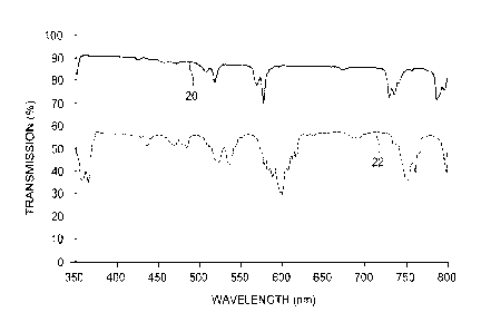
[0022] FIG. 2 is a graph of transmission in a visible spectrum of Nd203 and
NdF3;
[0023] FIG. 3 is a color space diagram demonstrating how Nd203 and NdF3
compounds blended
into an optical component (such as silicone or polycarbonate) and deposited on
a standard LED
package (such as 80CRI with 3000K CCT) can shift a color point of the light
source along
vectors defined by the spectral absorption of the Nd203 and NdF3 compounds;
4
CA 03007011 2018-05-30
WO 2017/100190 PCT/US2016/065149
[0024] FIG. 4a is a graph of transmission in a visible spectrum of Nd compound
mixes
comprising different amounts of Nd203 and NdF3 according to an embodiment of
the invention;
[0025] FIG. 4b is a graph of simulated emission of lamps (such as LED lamps)
in a visible
spectrum utilizing filters with various Nd compound mixes shown in FIG. 4a
according to an
embodiment of the invention;
[0026] FIG. 5 is a color space diagram comparing color points of a standard
3000K LED lamp
with simulated color points of LED lamps comprising filters with various Nd
compound mixes
shown respectively in FIGS. 4a and 4b according to an embodiment of the
invention;
[0027] FIGS. 6a-6d are non-limiting examples of a LED-based lighting
apparatus, incorporating
a ND-F compound (or more generally Nd-X-F compound as described herein) along
with a
phosphor to impart favorable visible absorption/generation characteristics
according to various
embodiments of the invention;
[0028] FIG. 7 is a cross-sectional view of a LED-based lighting apparatus in
accordance with
one embodiment of the invention;
[0029] FIG. 8 is a cross-sectional view of a LED-based lighting apparatus in
accordance with
another embodiment of the invention;
[0030] FIG. 9 is a perspective view of a LED-based lighting apparatus in
accordance with a
further embodiment of this invention;
[0031] FIG. 10 is a perspective view of a LED-based lighting apparatus in
accordance with one
further embodiment of this invention.
DETAILED DESCRIPTION
[0032] A new apparatus such as a lighting apparatus is presented herein, the
apparatus
comprising at least one LED (or OLED) module configured to generate a visible
light such as
white light, and at least one component such as an optical component
comprising multiple (two
or more) compounds, each comprising neodymium (Nd) and at least one compound
comprising
fluorine (F) for imparting a desired color filtering effect to provide a
desired light spectrum,
where a color of the desired light spectrum in a color space is determined by
relative amounts of
the two or more compounds in the at least one component.
CA 03007011 2018-05-30
WO 2017/100190 PCT/US2016/065149
[0033] For example, according to one embodiment of the invention, the at least
one component
(optical component) may be a polymer base material (such as silicone,
polycarbonate and the
like) comprising two compounds: a first compound may be neodymium oxide
(Nd203) and a
second compound may be neodymium fluoride (NdF3), as this case is described in
detail herein.
The neodymium compounds absorb yellow light in the 560-600nm range, which
alters the color
point of the LED system. The addition of a single compound can move the color
point along a
line in the CIE 1931 color space (with chromaticity coordinates CCX and CCY).
By using two
or more compounds the color point can be moved anywhere within an area of the
CIE color
space (hereinafter "color space"). This allows for greater customization of
the color of the LED
system for a particular application as demonstrated in FIG. 3 herein.
[0034] In other words, the neodymium compounds (such as Nd203 and NdF3 in the
above
example) can be added in various amounts to change the composition of the
optical component
for controlling the color point of the resulting light. The different
absorption spectra of the two
(or more) components result in movement of the color point of the LED system
in different
directions (i.e., in both CCX and CCY directions) when each component is
added. Then color
point movement vectors of the multiple compounds comprising Nd and F,
described herein, can
bound an area within the CIE color space, inside of which any color point can
be achieved with
the same LED, by varying the relative amounts of the two or more compounds, as
described
herein.
[0035] According to another embodiment, a scattering element, such as titania
(TiO2), alumina
(Al2O3), silica (SiO2) or the like, may be added to the polymer base to
increase the diffusivity of
the multiple Nd and F compounds in the optical component. Variation of three
variables (e.g.,
weight loading of TiO2, NdF3, and Nd203 for the above example) may allow
creation of a wide
variety of specialized optical components for achieving a desired light
spectrum and distribution.
[0036] Moreover, according to one embodiment of the invention, at least one
compound (or
more than one) may comprise elements of neodymium (Nd) and fluorine (F), and
optionally
comprising one or more other elements. Typically such compound comprises Nd'
ions and F"
ions. For the purpose of this invention, a "Nd¨F compound" should be broadly
construed to
include compounds comprising neodymium and fluoride and optionally other
elements.
[0037] According to a further embodiment, the component may include a
composite/encapsulating layer on a surface of the LED (OLED) chip so that
multiple compounds
comprising Nd and F disclosed herein, can be blended (dispersed) in that
encapsulating layer,
6
282201-4
e.g., along with a phosphor, to achieve favorable visible absorption profiles.
The
composite/encapsulating layer may be formed using a low temperature glass, a
polymer (such as
polycarbonate), a polymer precursor, a silicone (polymer) or silicone epoxy
resin or precursor,
and the like.
[0038] According to another embodiment, the optical component may be a
transparent,
translucent reflective or transflective (partially reflective and
transmitting) substrate, and a
coating on a surface of the substrate comprising multiple Nd and F components
described herein,
can apply a color filtering effect to the visible light, generated by the LED
module, while it is
passing through the optical component, e.g., to filter the visible light in
the yellow light
wavelength range, for example, for wavelengths from about 560 nm to about 600
nm to provide
a desired light spectrum.
[0039] Furthermore, the transparent or translucent substrate of the optical
component may be a
diffuser, such as a bulb, a lens and an envelope enclosing at least one LED
chip. Moreover, the
substrate may be a reflective substrate, and the LED chip can be arranged
outside of the
substrate. The multi-compound coating (comprising Nd and F multiple compounds
described
herein) may be disposed on a surface of the substrate, and the thickness of
the coating should be
sufficient to achieve the color filtering effect. The thickness may typically
be within a range
from 50 nm to 1000 microns, with a preferred thickness being between 100 nm to
500 microns.
[0040] The resultant devices can exhibit improvement of light parameters using
filtering with
Nd and Nd-F compounds/materials having intrinsic absorption in the visible
region between
about 530 nm and 600 nm to enhance CSI (color saturation index), CRI (color
rendering index),
R9 (color rendering value) revealness (lighting preference index, LPI) and the
like. R9 is
defined as one of 6 saturated test colors not used in calculating CRI. The
"revealness" is a
parameter of the emitted light based on a version of the LPI, which is
described in co-pending,
commonly owned International application PCT/US2014/054868, filed September 9,
2014
(published as W02015/035425 on March 12, 2015).
[0041] In one embodiment, at least one of the multiple compounds described
herein may
including Ne ions and F- ions and may be a Nd¨F compound or a Nd¨X¨F compound.
As
used herein, the "Nd¨F compound" should be broadly construed to include
compounds including
neodymium and fluoride and optionally other elements. Such compounds
comprising
neodymium and fluoride may comprise neodymium fluoride, or neodymium
oxyfluoride (e.g.,
NdO.Fy where 2x+y=3, such as Nd403F6) or neodymium fluoride comprising
adventitious water
7
Date Regue/Date Received 2023-05-17
CA 03007011 2018-05-30
WO 2017/100190 PCT/US2016/065149
and/or oxygen, or a neodymium hydroxide fluoride (e.g., Nd(OH)aFb where ad-
b=3), or
numerous other compounds comprising neodymium and fluoride which will be
become readily
apparent from the following description.
[0042] In some embodiments, one of the multiple compounds may be NdF3 or NdFO.
For the
Nd¨X¨F compound, X is at least one element selected from the group consisting
of: elements
that form compounds with neodymium, such as, oxygen, nitrogen, sulfur and
chlorine, or at least
one metallic element that form compounds with fluorine, such as Na, K, Al, Mg,
Li, Ca, Sr, Ba,
and Y, or combinations of such elements, said metallic elements being
different from
neodymium. Particular examples of Nd¨X¨F compounds may include: neodymium
oxyfluoride
(Nd¨O¨F) compounds; Nd¨X¨F compounds in which X may be Mg and Ca or may be Mg,
Ca
and 0; as well as other compounds containing Nd¨F, including perovskite
structures doped with
neodymium. Certain Nd¨X¨F compounds may advantageously enable broader
absorption at
wavelengths of about 580 nm.
[0043] As stated above, one component/optical component may be a polymer base
material
(such as silicone, polycarbonate and the like) comprising, for example, two
compounds Nd203
and NdF3. FIG. 2 is a graph of transmission in a visible spectrum of Nd203
(1.0% in 1.3 mm
thick silicone having refractive index of 1.54) represented by a curve 22, and
of NdF3 (2.9% in
1.3 mm thick silicone having refractive index of 1.54) represented by a curve
20. It can be seen
that the respective materials share many of the similar absorptive features,
especially in the
yellow (e.g., about 570 nm - about 600 nm) region. The different absorption
peaks shown in
FIG. 2 drive different color shift vectors of each component (Nd203 and NdF3)
in color space as
further demonstrated in FIG. 3, By combining the two compounds, color points
can be achieved
that cannot be achieved with a single Nd compound or with Nd:glass (Nd203 in
SiO2).
[0044] In use, one may encapsulate an LED chip/die with an encapsulant (e.g.,
silicone, epoxy,
acrylic, or the like); the encapsulant may comprise Nd203 and NdF3 material or
in general Nd
and F based compounds as described herein, such that, e.g., Nd203 and NdF3 in
silicone can be
deposited directly on the LED chip or on the array of LED chips (e.g., chip-on-
board array, COB
array) as further detailed herein.
[0045] FIG. 3 is a color space diagram demonstrating how Nd203 and NdF3
compounds
blended into an optical component (such as silicone or polycarbonate) and
deposited on a
standard LED package (such as 80CRI with 3000K CCT) can shift a color point of
the light
source along vectors 30 and 32 respectfully defined by the spectral absorption
of the Nd203 and
NdF3 compounds.
8
CA 03007011 2018-05-30
WO 2017/100190 PCT/US2016/065149
[0046] As it is clear from the diagram in FIG. 3, this system theoretically
can allow any color
point in a triangle ABC to be created from a standard 3000 K LED by varying
relevant amounts
of Nd203 and NdF3 compounds, i.e., shifting color point of emitter along
vectors 30 and 32
defined by the spectral absorption of the Nd203 and NdF3 compounds
respectively. However,
since large energy losses due to high filtering are undesirable, this system
may be practically
limited to a smaller area 34, for example 12 MacAdam ellipses, or arbitrarily
chosen some other
area size, based on the application and the end user's willingness to
sacrifice LPW (lumen per
watt) to achieve a color point very far from the starting color. The area 34
is confined by lines
BD, BE and a curve 36. Any of the practical color points in the area 34 can be
achieved over a
wide range of relative amounts and diffusion levels of the Nd203 and NdF3
compounds, allowing
for application of a given color point in different LED systems which require
different beam
shaping characteristics of the optics. By comparison, the addition of the Nd
glass (conventional
method) allows movement of the color point only to a single point 38 (or along
a vector if the
thickness of the glass is varied). Figures 4a, 4b and 5 demonstrate further
examples for
practicing embodiments disclosed herein.
[0047] FIG. 4a is an exemplary graph of transmission in a visible spectrum of
Nd compound
mixes comprising different amounts of Nd203 and NdF3 in a silicone tape
according to an
embodiment of the invention. A curve 42a corresponds to 1.3 mm thick silicone
tape comprising
4% of NdF3 and 1% of Nd203, a curve 44a corresponds to 1.3 mm thick silicone
tape
comprising 5% of NdF3 and 0.5% of Nd203, a curve 46a corresponds to 1.3 mm
thick silicone
tape comprising 3.% of NdF3 and 0.5% of Nd203, and a curve 48a corresponds to
1.3 mm thick
silicone tape comprising 3.5% of NdF3 and 1.8% of Nd203.
[0048] FIG. 4b is a graph of simulated emission of lamps (such as LED lamps)
in a visible
spectrum utilizing filters with various Nd compound mixes shown in FIG. 4a
according to the
embodiment of the invention. In FIG. 4b a curve 42b is for simulated LED lamp
with the1.3 mm
thick silicone tape comprising 4% of NdF3 and 1% of Nd203, a curve 44b is for
simulated LED
lamp with the 1.3 mm thick silicone tape comprising 5% of NdF3 and 0.5% of
Nd203, a curve
46b is for simulated LED lamp with the 1.3 mm thick silicone tape comprising
3% of NdF3 and
0.5% of Nd203, and a curve 48b is for simulated LED lamp with the 1.3 mm thick
silicone tape
comprising 3.5% of NdF3 and 1.8% of Nd203.
[0049] FIG. 5 is a color space diagram comparing color points of a standard
3000K LED lamp
with color points of LED lamps comprising filters with various Nd compound
mixes shown
respectively in FIGS. 4a and 4b according to the embodiment of the invention.
In FIG. 5 a color
9
282201-4
point 52 is for simulated LED lamp with the1.3 mm thick silicone tape
comprising 4% of NdF3
and 1% of Nd203, a color point 54 is for simulated LED lamp with the 1.3 mm
thick silicone
tape comprising 5% of NdF3 and 0.5% of Nd203, a color point 56 is for
simulated LED lamp
with the 1.3 mm thick silicone tape comprising 3% of NdF3 and 0.5% of Nd203,
and a color
point 58 is for simulated LED lamp with the 1.3 mm thick silicone tape
comprising 3.5% of
NdF3 and 1.8% of Nd203.
[0050] FIGS. 4a, 4b and 5 demonstrate how changing relative amounts of NdF3
and Nd203 in a
filtering component of an (LED) lamp can modify a color temperature of the
lamp and modify its
emission spectrum (e.g., an absorption peak around 570-600 nm wavelength
range) to provide a
desired lamp spectrum (e.g., "whitening" of the light source") with the
desired color
temperature, and an adequate level of the transmitted lumen power, to be able
to further improve
other light parameters such as CSI, CRI, R9 and revealness. The "revealness"
is a parameter of
the emitted light based on a version of the LPI, which is described in co-
pending, commonly
owned International application PCT/US2014/054868, filed September 9, 2014
(published as
W02015/035425 on March 12, 2015).
[0051] In a further embodiment, the multiple Nd and F compounds of
corresponding relative
amounts may be blended into an encapsulating material along with one or more
luminescent
materials, such as phosphors. For example, the Nd and F multiple compounds of
corresponding
relative amounts may be blended with a yellow-green phosphor and/or a red
phosphor. For
example, the multiple Nd and F compounds may be blended with a Ce-doped YAG
phosphor
and/or a conventional red nitride phosphor, such as a Eu2+-doped CaAlSiN red
phosphor. In
another example, the Nd and F multiple compounds can be blended with YAG:Ce
phosphor and
a red nitride phosphor in silicone, encapsulating a blue/ultraviolet-emitting
LED.
[0052] FIGS. 6a-6d demonstrate different non-limiting examples of a LED-based
lighting
apparatus 60a, 60b, 60c and 60d respectfully, incorporating the Nd and F
multiple compounds,
as described herein, along with the phosphor to achieve favorable visible
absorption/generation
characteristics, according to various embodiments of the invention. In FIGS.
6a-6d the
LED-based lighting apparatus 60a, 60b, 60c or 60d includes a dome 62 that can
be an optically
transparent or translucent substrate enclosing an LED chip 65 mounted on a
printed circuit board
(PCB) 66. Leads provide current to the LED chip 65, thus causing it to emit
radiation. The LED
chip may be any semiconductor light source, especially a blue or ultraviolet
light source that is
capable of producing white light when its emitted radiation is directed onto
the phosphor. In
particular, the semiconductor light source may be a blue/ultraviolet (UV)
emitting LED based on
Date Regue/Date Received 2023-05-17
CA 03007011 2018-05-30
WO 2017/100190 PCT/US2016/065149
a nitride compound semiconductor generalized as IniGajAlkN, where i, j and k
are integers each
having a value one or zero (include for example InGaN, AIN, AlGaN, AlGaInN
device
structures) having an emission wavelength greater than about 200 nm and less
than about 550
nm, More particularly, the chip may be a near-UV or blue emitting LED having a
peak emission
wavelength from about 400 to about 500 nm. Even more particularly, the chip
may be a blue
emitting LED having a peak emission wavelength in a range about 440-460 nm.
Such LED
semiconductors are known in the art.
[0053] According to one embodiment shown in FIG. 6a, a polymer composite
layer
(encapsulant compound) 64a can comprise the Nd and F multiple compounds, as
described
herein, blended with a phosphor to impart favorable visible
absorption/generation characteristics
according to various embodiments described herein. This compound layer 64a can
be disposed
directly on a surface of the LED chip 65 and radiationally coupled to the
chip. "Radiationally
coupled" means that radiation from the LED chip is transmitted to the
phosphor, and the
phosphor emits radiation of a different wavelength. In a particular
embodiment, the LED chip
65 may be a blue LED, and the polymer composite layer can include a blend of
the multiple Nd
and F compounds of corresponding relative amounts with a yellow-green phosphor
such as a
cerium-doped yttrium aluminum garnet, Ce:YAG. The blue light emitted by the
LED chip mixes
with the yellow-green light emitted by the phosphors of polymer composite
layer, and the net
emission appears as white light which is filtered by the Nd and F multiple
compounds. Thus
LED chip 65 may be enclosed by the encapsulant material layer 64a. The
encapsulant material
may be a low-temperature glass, a thermoplastic or theitnoset polymer or
resin, or a silicone or
epoxy resin. The LED chip 65 and the encapsulant material layer 64a may be
encapsulated
within a shell (restricted by the dome 62). Alternatively, the LED apparatus
60a may only
include the encapsulant layer 64a without the outer shell/dome 62. In
addition, scattering
particles may be embedded in the encapsulant material to increase diffusivity
of the Nd and F
multiple compounds, as described herein. The scattering particles may be, for
example, alumina
(A1203), silica (SiO2) or titania (TiO2). Also, the scattering particles can
effectively scatter the
directional light emitted from the LED chip, preferably with a negligible
amount of absorption.
[0054] To form a polymer composite layer that includes the multiple Nd and
F compounds of
corresponding relative amounts, described herein, on a surface of an LED chip,
the particles may
be dispersed in a polymer or polymer precursor, particularly a silicone,
polycarbonate, silicone
epoxy resin, or precursors therefor. Such materials are well known for LED
packaging. The
dispersion mixture can be coated on the chip by any suitable process, for
example using injection
molding (or casting and extruding the optical component or similar
techniques), and particles
11
CA 03007011 2018-05-30
WO 2017/100190 PCT/US2016/065149
having a larger density or particle size, or a larger density and larger
particle size, preferentially
settle in the region proximate the LED chip, forming a layer having a graded
composition.
Settling may occur during the coating or curing of the polymer or precursor,
and may be
facilitated by a centrifuging process, as known in the art. It is further
noted that the parameters of
dispersion of the phosphor and the Nd and F multiple compounds, e.g.,
including particle density
and size and process parameters, can be chosen to provide the phosphor
material being closer to
the LED chip 65 than the Nd and F multiple compounds, in order to provide an
appropriate
filtering by the Nd and F multiple compounds of the light generated by the
phosphor component.
[0055] In an alternative exemplary embodiment shown in FIG. 6b, the phosphor
layer 64b may
be a conventionally fabricated encapsulant layer, and a separate encapsulant
layer 68b with the
Nd and F multiple compounds may be deposited on top of the phosphor layer 64b,
e.g., using the
appropriate conventional deposition/particle dispersion technique in a polymer
or polymer
precursor.
[0056] In a further exemplary embodiment shown in FIG. 6c, a composite layer
68c comprising
the Nd and F multiple compounds can be coated on an outer surface of the dome
(shell) 62. The
perfoirnance of the coated layer 68b is similar to the performance of the
encapsulant layer 68b
with the Nd and F multiple compounds in FIG. 6b. Alternatively, the coating
68c in FIG. 6c can
be deposited on an inner surface of the dome 62. More implementation details
regarding coating
of the dome/substrate will be discussed in reference to Figures 7-10. It is
noted that the dome 62
itself can be transparent or translucent.
[0057] In yet a further exemplary embodiment, as shown in FIG. 6d, the dome
(shell) 62 can
be used to deposit multiple Nd and F compound composite layer/coating 68d on
the outer
surface of the dome 62 and a phosphor coating layer 64d on the inner surface
of the dome 62. It
is further noted that there may be different variations of this approach. For
example, both
coatings 64d and 68d may be deposited on one surface (outer or inner surface)
of the dome 62
with the phosphor coating 64d being closer than the coating 68d to the LED
chip 65. Also,
coatings 64d and 68d (when deposited on one surface of the dome 62) can be
combined in one
layer similar to the encapsulant compound layer 64a in FIG. 6a. It is noted
that the dome 62
itself can be transparent, translucent or transflective, in order to implement
different variations of
the example shown in FIG. 6d.
[0058] Below are several non-limiting examples of a LED-based lighting
apparatus using the
coating containing the Nd and F multiple compounds, described herein causing a
desired color
filter effect.
12
CA 03007011 2018-05-30
WO 2017/100190 PCT/US2016/065149
[0059] FIG. 7 is a LED-based lighting apparatus suitable for area lighting
applications in
accordance with one embodiment of the invention. The LED-based lighting
apparatus (which
may also be referred to as a "lighting unit" or "lamp") is an LED lamp 70
configured to provide a
nearly omnidirectional lighting capability. As shown in FIG. 7, the LED lamp
70 includes a
bulb 72, a connector 74, and a base 76 between the bulb 72 and the connector
74, and a coating
78 on an outer surface of the bulb 72. The coating 78 includes the Nd and F
multiple
compounds described herein. In other embodiments, the bulb 72 can be replaced
by other
transparent or translucent substrates. Alternatively, the coating 78 may be
coated on an inner
surface of the bulb 72 which can be transparent or translucent.
[0060] FIG. 8 is a LED-based lighting apparatus 80 in accordance with a
further embodiment of
this invention. As shown in FIG. 8, the LED-based lighting apparatus is a
ceiling lamp 80 (LED
chip is not shown). The ceiling lamp 80 includes a hemispherical substrate 82
and a coating 88
containing the Nd and F multiple compounds described herein; the coating 88 is
on an inner
surface of the hemispherical substrate 82. Alternatively, the coating 88 may
be coated on an
outer surface of the hemispherical substrate 82 which can be transparent or
translucent.
[0061] FIG. 9 is a LED-based lighting apparatus in accordance with a further
embodiment of
this invention. As shown in FIG. 9, the LED-based lighting apparatus is a lens
90, and the lens
90 includes a flat substrate 92. In this embodiment, the flat substrate 92
includes the Nd and F
multiple compound coating (not shown) on an outer surface thereof
[0062] FIG. 10 is a LED-based lighting apparatus 100 in accordance with one
further
embodiment of the invention. The LED-based lighting apparatus 100 includes a
bulb 102, at
least one LED chip 105 and a reflective substrate 106. The reflective
substrate 106 is configured
to reflect the visible light generated by the LED chip 105. In certain
embodiments, the reflective
substrate 106 includes the Nd and F multiple compound coating (not shown) on
an outer surface
thereof for providing the desired filtering. In Fig. 10 the dome (102) can be
constructed of a
diffusing material, so that a certain amount of light from the LEDs will pass
through, and a
certain amount will be reflected back into the cavity (these amounts depend on
how highly
diffusing the dome material is). The reflected light will either reflect
specularly or diffusely,
depending on the diffusivity of the dome 102. These diffuse and/or specular
reflections from the
dome 102 will be incident upon the reflective substrate 106 coated according
to one of the
embodiment described herein. Alternatively the dome 102 can be constructed
from a broadband
semi-reflective material to provide the same functionality.
13
CA 03007011 2018-05-30
WO 2017/100190 PCT/US2016/065149
[0063] The coating materials described herein, including a compound containing
Nd3+ ions and
F- ions, may have little optical scattering (diffusion) effect; or,
alternatively, may cause
considerable optical scattering on light passing therethrough. To increase a
scattering angle, the
coating may include discrete particles of an organic or inorganic material.
Alternatively, the
organic or inorganic material can be solely made up of discrete particles of
the Nd and F
multiple compounds described herein, and/or made up of a mixture of discrete
particles of the
Nd and F multiple compounds and particles formed of at least one other
different material.
[0064] In one embodiment, a suitable particle size for the organic or
inorganic material can be
from about 1 nm to about 10 microns. For the LED lamp 70 shown in FIG.7, in
order to
maximize a scattering angle so that the LED lamp 70 could achieve omni-
directional lighting,
the particle size may be chosen to be much less than 300nm to maximize
efficiency of a
Rayleigh scattering.
[0065] Although not intended to be limiting, the Nd and F multiple compound
coating may be
applied by, for example, spray coating, roller coating, meniscus or dip
coating, stamping,
screening, dispensing, rolling, brushing, bonding, electrostatic coating or
any other method that
can provide a coating of even thickness. The following will describe three non-
limiting
examples of how to provide the Nd and F multiple compound coating on the
substrate.
[0066] In one embodiment, as shown in FIG. 7, the coating 37 may be coated on
the bulb 72 by
a bonding method. The LED lamp 70 can include a bonding layer (not shown)
between the bulb
72 and the coating 78, and the bonding layer may include an organic adhesive
or an inorganic
adhesive. The organic adhesive can include an epoxy resin, an organic silicone
adhesive, an
acrylic resin, etc. The inorganic adhesive can include a silicate inorganic
adhesive, a sulfate
adhesive, a phosphate adhesive, an oxide adhesive, a boric acid salt adhesive
etc.
[0067] In another embodiment, as shown in FIG. 7, the coating 78 may be coated
on the outer
surface of the bulb 72 by a spray-coating method. Firstly, a liquid mixture
containing, for
example, Nd203 and NdF3 compounds of corresponding relative amounts, silicone
dioxide,
dispersant such as DISPEX A40, water and optionally TiO2 or A1203 is formed.
Subsequently,
the formed liquid mixture is sprayed onto the bulb 72. Finally, the bulb 72 is
cured to obtain the
coated LED lamp 70.
[0068] In one embodiment, as shown in FIG.7, the coating 78 may be coated onto
the outer
surface of the bulb 72 by an electrostatic coating method. Firstly,
electrically charged powder
14
CA 03007011 2018-05-30
WO 2017/100190 PCT/US2016/065149
consisting, for example, Nd203 and NdF3 compounds of corresponding relative
amounts, SiO2
and A1203 is produced. Subsequently, the powder is coated onto the bulb 72
which is oppositely
charged.
[0069] In another embodiment of the invention, both the spray coating method
and the
electrostatic coating method may use materials without organic solvent or
organic compound,
which can extend the service life of the LED light apparatus and avoid the
discoloration typically
caused by sulfonation.
[0070] In a further embodiment, to promote refraction of the light to achieve
a white reflective
appearance, the coating further may include an additive having a higher
refractive index relative
to the multiple Nd and F compounds. The additive can be selected from at least
one of metal
oxides or non-metal oxides, such as TiO2, SiO2 and A1203.
[0071] Unless defined otherwise, technical and scientific terms used herein
have the same
meaning as is commonly understood by one having ordinary skill in the art to
which this
disclosure belongs. The terms "first", "second", and the like, as used herein,
do not denote any
order, quantity, or importance, but rather are employed to distinguish one
element from another.
Also, the terms "a" and "an" do not denote a limitation of quantity, but
rather denote the
presence of at least one of the referenced items. The use of "including,"
"comprising" or
"having" and variations thereof herein are meant to encompass the items listed
thereafter and
equivalents thereof, as well as additional items. The terms "connected" and
"coupled" are not
restricted to physical or mechanical connections or couplings, and can include
electrical and
optical connections or couplings, whether direct or indirect.
[0072] Furthermore, the skilled artisan will recognize the interchangeability
of various features
from different embodiments. The various features described, as well as other
known equivalents
for each feature, can be mixed and matched by one of ordinary skill in this
art, to construct
additional systems and techniques in accordance with principles of this
disclosure.
[0073] In describing alternate embodiments of the apparatus claimed,
specific terminology is
employed for the sake of clarity. The invention, however, is not intended to
be limited to the
specific terminology so selected. Thus, it is to be understood that each
specific element includes
all technical equivalents that operate in a similar manner to accomplish
similar functions.
CA 03007011 2018-05-30
WO 2017/100190 PCT/US2016/065149
[0074] It is to be understood that the foregoing description is intended to
illustrate and not to
limit the scope of the invention, which is defined by the scope of the
appended claims. Other
embodiments are within the scope of the following claims.
[0075] It is noted that various non-limiting embodiments described and
claimed herein may
be used separately, combined or selectively combined for specific
applications.
[0076] Further, some of the various features of the above non-limiting
embodiments may be
used to advantage, without the corresponding use of other described features.
The foregoing
description should therefore be considered as merely illustrative of the
principles, teachings and
exemplary embodiments of this invention, and not in limitation thereof.
16