Note : Les descriptions sont présentées dans la langue officielle dans laquelle elles ont été soumises.
CA 03007154 2018-06-01
1
Method for producing a security element and transfer film
The invention relates to a method for producing a security element, and a
transfer
film, in particular a hot-stamping film, for the transfer of one or more
multilayer bodies
onto a target substrate.
Transfer films, in particular hot-stamping films, amongst others are used for
the
application of a security element to security documents, for example
passports, credit
cards or banknotes. A security element is applied to a substrate, which is
formed by
the decorative ply of a hot-stamping film. The security element comprises, for
example, an in particular transparent varnish layer, into which a structure,
in
particular for producing an optically variable effect, in particular a
structure with
optically diffractive action, is molded. For example, the transparent varnish
layer can
be further provided with a reflection-increasing layer, which is a metal layer
or a
dielectric layer. The security element further has an adhesive layer, by means
of
which the security element is fixed to the substrate. For this the hot-
stamping film is
placed on the substrate and, by means of a stamping die, under the action of
heat
and pressure, is pressed onto the cover ply in the region in which the
decorative ply
of the hot-stamping film is to be transferred onto the substrate. When the
carrier film
of the hot-stamping film is removed, this partial region of the decorative ply
further
adheres firmly to the substrate, and the other partial regions of the
decorative ply are
removed together with the carrier film.
In the case of such a transfer of the decorative ply of a hot-stamping film
from a
carrier film onto a substrate, the decorative ply of the stamping film is torn
along the
boundary line which defines the partial region of the decorative ply to be
transferred.
This boundary line can be defined for example by the circumferential outer
edges of
CA 03007154 2018-06-01
2
a stamping die as the stamping contour. In particular when transfer films with
thicker
layers and layers with specific properties are used, for example layers with
particularly high toughness and/or brittleness, this can lead to fraying of
the edges
(as positive and/or negative mold).
In order to avoid these problems, it is known to adhesively bond a further
carrier ply
as auxiliary carrier to the carrier ply of the hot-stamping film in the region
of the partial
regions to be transferred and to at least partially punch through the hot-
stamping film
along the tear of the partial regions to be transferred (so-called patches).
The partial
regions not required can then be detached. The remaining partial regions can
subsequently be stamped with sharp edges.
In this technology, there is the problem that the partially applied UV
adhesive used
therein is applied in a region that is somewhat larger than the punched patch
in order
to compensate for register variations in the case of UV adhesive printing, so
that the
complete patch is in every case covered by the UV adhesive. An adhesive border
therefore exists around the patch in the punched-out state.
By register or registration and register accuracy or registration accuracy is
meant a
positional accuracy of two or more elements and/or layers, here in particular
of the
substrate and the stamping film and/or the decorative section relative to each
other.
The register accuracy is to vary within a predetermined tolerance, which is to
be as
small as possible. At the same time, the register accuracy of several elements
and/or
layers relative to each other is an important feature in order to increase the
process
reliability. The positionally accurate positioning can be effected in
particular by means
of sensorily, preferably optically detectable registration marks or register
marks.
These registration marks or register marks can either represent specific
separate
elements or regions or layers or themselves be part of the elements or regions
or
layers to be positioned.
CA 03007154 2018-06-01
3
This UV adhesive performs a double function. During the application of the
film, the
UV adhesive is intended to stick the auxiliary carrier and the carrier firmly
together in
order to guarantee the removal of the auxiliary carrier and the carrier from
the applied
transfer ply at the same time. During the processing/production of the film,
the UV
adhesive is intended to fix the partial region to be transferred in situ (for
example in
the case of winding procedures), but also to allow the removal of the partial
regions
not required; i.e. its adhesive strength, in particular at the adhesive
border, should
not be too great.
io The UV adhesive is therefore only fully cured in part, i.e. although
this adhesive is
UV-cured it has a residual tack and this subsequently appears in a disruptive
manner
during the further application, in particular in the region of the protruding
adhesive
border mentioned above. The residual tack can also first be formed by the
introduction of heat during the hot stamping or during other production steps,
for
is example in the case of previously insufficient curing or generally
inadequate
temperature resistance of the adhesive. The mentioned residual tack can,
however,
also occur in the case of UV adhesives which have been largely completely
cured.
Furthermore, the adhesion of the UV adhesive between auxiliary carrier and
carrier
20 during the application is not always sufficient on its own to transfer
the transfer plies,
and the entire patch is then transferred, including the carrier ply, which
detaches from
the auxiliary carrier in an undesired manner.
The object of the invention is now to specify an improved method for producing
a
25 decorative element or a security element, and an improved transfer film.
This object is achieved by a method with the features of claim 1 and a
transfer film
with the features of claim 46.
30 Such a method for producing a security element is characterized in that
in the
method a base film is provided, which has a first carrier film and a single-
or
CA 03007154 2018-06-01
4
multilayered decorative ply,
- wherein a first adhesive layer is applied to a second carrier film and a
second
adhesive layer is applied to the surface of the first carrier film facing away
from the
decorative ply or wherein the second adhesive layer is applied to the surface
of the
first carrier film facing away from the decorative ply and the first adhesive
layer is
applied to the second adhesive layer,
- and wherein the second carrier film is applied to the first carrier film
such that the
first adhesive layer and the second adhesive layer are arranged between the
first
carrier film and the second carrier film,
io - and wherein the first adhesive layer is activated in a first region
which at least
partially covers at least one first partial region of the base film, but the
first adhesive
layer is not activated, not provided, only partially provided or deactivated
in a second
region adjoining this region,
- wherein the first carrier film is at least partially severed along the
boundary line
defining the at least one first partial region and separating the at least one
first partial
region from a second partial region of the base film, and
- wherein a second part of the base film comprising the second partial region
is
removed from the second carrier film, wherein in the at least one first
partial region
the base film adheres to the second carrier film because of the activated
first
adhesive layer and a first part of the base film comprising the at least one
first partial
region remains on the second carrier film.
An adhesive can be a polymer, for example a varnish as a liquid, paste-like or
also
powdered coating material, which is deposited thinly on surfaces and forms an
in
particular continuous film by chemical and/or physical processes.
A transfer film, in particular a hot-stamping film, is thus obtained for the
transfer of
one or more multilayer bodies onto a target substrate, wherein the transfer
film has a
base film, which has a first carrier film and a single- or multilayered
decorative ply,
wherein
- the transfer film further has a second carrier film with a first adhesive
layer and a
CA 03007154 2018-06-01
second adhesive layer applied to the surface of the first carrier film facing
away from
the decorative ply, wherein the first adhesive layer and the second adhesive
layer are
arranged between the first carrier film and the second carrier film, and
wherein
- the first adhesive layer is activated in a first region at least
partially covering at least
5 one first partial region of the base film, with the result that the base
film adheres to
the second carrier film in the at least one first partial region, but is not
activated, not
provided, only partially provided or deactivated in a second partial region
adjoining
the at least one first partial region, and wherein
- the first carrier film is severed along the boundary line defining the at
least one first
partial region and separating the at least one first partial region from a
second partial
region of the base film and a part of the base film comprising the second
partial
region is removed from the second carrier film.
It is hereby possible to prepare a security element which can be transferred
by
means of a conventional transfer method onto a security document, for example
a
banknote or an ID document, and which prevents a "fraying" caused by the
decorative ply breaking in the edge region of the transferred multilayer body.
It is
further possible that the adhesive and structural properties of the decorative
ply can
be selected substantially independently of the requirements of the transfer
process
and in this way, for example, the optical properties, the resistance to
environmental
influences as well as the security against forgery and manipulation of the
security
element can be further improved. In particular, particularly brittle or thick
or tough
layers in the decorative ply can thus be transferred. The method according to
the
invention is further characterized in that the registration accuracy with
which security
elements can be transferred onto a target substrate is further improved.
Within the meaning of the invention, by transfer film is quite generally meant
a film
which has a carrier ply or carrier film and a transfer ply, wherein the
transfer ply,
which in particular has at least one decorative ply, can be detached from the
carrier
ply. The detachment is effected in particular in a stamping device, wherein at
least a
CA 03007154 2018-06-01
6
part of the transfer film is transferred onto a substrate to be decorated and
subsequently the carrier ply is removed from the applied transfer ply.
The base film can be formed both as a transfer film and as a laminating film.
If the
base film is formed as a transfer film, then in particular the decorative ply
of the base
film is transferred onto a substrate and subsequently the first carrier film
is removed
from it and preferably remains on the second carrier film. Here a detachment
layer is
particularly preferably arranged between the decorative ply and the first
carrier film.
lo If the base film is formed as a laminating film, then in particular the
decorative ply and
the first carrier film of the base film are transferred onto a substrate and
subsequently
the second carrier film is removed from it. Here a detachment system is
particularly
preferably arranged between the first and the second carrier film.
Furthermore, different shapes of the transfer film can be transferred with a
uniform
die shape. It is also possible to transfer several neighboring, isolated
patches by
means of a single die. The outer shape of the patch need not match the outer
shape
of the hot-stamping die. Here the hot-stamping die is preferably selected
larger than
the part of the base film to be transferred. For example, a patch in the shape
of a star
is transferred with a larger round die that more than completely covers the
star. In
addition to a hot-stamping die with which a hot stamping is carried out by
means of
stamping pressure and heat, an ultrasonic stamping die with correspondingly
designed thrust bearing can also be used, with which a hot stamping is carried
out by
means of stamping pressure and ultrasound as an alternative form of energy. It
is
likewise possible to use a roll laminator, in particular a semi-rotary
laminator and/or
multi-roll laminator (for example for banknote applications several lamination
rollers
are arranged one behind another in a row). It is furthermore possible to bring
the first
carrier film close to the second carrier film printed with UV adhesive with
the aid of a
guide roller without pressing the two carrier films together. Additional,
successive
guide rollers then ensure the necessary contact between the two carrier films
before
the curing with UV light.
CA 03007154 2018-06-01
7
It is also possible that the second partial region is not coherent or also has
sub-
regions in which the entire composite film is removed. For example, in an
embodiment each patch can have at least one enclosed free space, for example a
hole in the center. The hole (in general all shapes are possible) with this
shape is for
example also produced during the punching procedure. The punching sheet has
two
punching heights, for example; one in order to sever only the decorative ply
for the
release of first regions and the optionally present mark region to be retained
and
another higher one in order to sever the entire composite film and thus to
produce a
hole. Lasers with different settings for kiss cutting and punching through is
also
possible in principle. The film fragments forming in the process are usually
pressed
out or blown out of the composite film. In this partial region the entire
composite film
is thus removed.
The advantages of such holes or perforations lie in an improvement in the
interlayer
adhesion when the partial region to be transferred lies between two cover
layers, in
particular in the later use of the security element. Furthermore, such a hole
can serve
as a replacement for and/or supplement to an optically transparent partial
region in
the motif. Through these holes or perforations the filigree character of the
partial
region to be transferred is enhanced and its protection against forgery is
thus also
improved. Possible motifs for the geometric design of the holes or
perforations are
alphanumeric characters such as for example A, B, D, 0, R, 8, 9 6, O.
The disadvantages of the single adhesive bonding with a UV adhesive named at
the
beginning can be overcome by the second adhesive layer. In particular,
adhesives
with different adhesive and/or activation properties can be used. The first
adhesive
layer merely serves to easily join the two carrier plies during processing.
The second
adhesive layer is preferably first thermally activated during the stamping and
then
increases the adhesion between the carrier plies, with the result that these
can be
detached together from the transferred part of the decorative ply after the
stamping.
In particular, this also makes it possible to apply the first adhesive layer
such that it
CA 03007154 2018-06-01
8
does not extend beyond the partial region to be transferred, with the result
that the
above-named problems due to residual tack do not arise later. The first
adhesive
layer is therefore preferably smaller than the partial region to be
transferred. In
principle the first adhesive layer fixes the partial region to be transferred
in situ,
wherein this can also be effected with a comparatively small adhesive spot.
The latter
can also be much smaller than the partial region to be transferred, with the
result that
the relative position between the partial region to be transferred and the
first
adhesive layer is not crucial.
The second carrier film can be both single-ply and multi-ply. The plies can
consist of
different or the same materials, for example of paper and/or fabric and/or
Teske
and/or the same or different plastic layers. They can be adhesively bonded to
each
other or for example produced by coextrusion or by multiple coatings.
Different adhesives, in particular differently activatable adhesives, are
therefore
preferably used for the first and second adhesive layer. In particular, it is
advantageous to use a radiation-activatable adhesive for the first adhesive
layer and
a thermally activatable adhesive for the second adhesive layer. A thermally
activatable adhesive can be both reactive and non-reactive. Multilayered
structures
are furthermore possible. In addition to radiation-activatable adhesives,
other reactive
types of adhesive are also possible, such as for example one- and two-
component
systems (epoxy systems and/or for example with isocyanates as polymerization
or
crosslinking initiator).
It is advantageous here if the second adhesive layer is activated when the
first part of
the base film is hot-stamped onto a substrate. Before the hot stamping, the
second
adhesive layer therefore preferably has no tack. During the hot stamping and
the
activation, the interlayer adhesion between the carrier plies is then
increased,
preferably by more than 50%, preferably more than 100%, particularly
preferably
more than 200%.
CA 03007154 2018-06-01
9
It is preferred if the hot stamping is effected at a temperature of from 80 C
to 300 C,
preferably from 100 C to 240 C, particularly preferably from 100 C to 180 C
and/or
with a stamping pressure of from 10 N/cm2 to 10,000 N/cm2, preferably from 100
N/cm2 to 5000 N/cm2 and/or with a stamping time of from 0.01s to 2s,
preferably from
0.01s to 1s.
It is further advantageous if the second adhesive layer is dried before the
second
carrier film is applied to the base film. It is hereby ensured that the second
adhesive
layer has no tack before the hot stamping. Varying degrees of surface coverage
of
the second adhesive layer (for example different degrees of surface coverage
in the
inner or outer region in the first partial region) can also be used. It is
furthermore
advantageous if the second adhesive layer is applied in a grid, in particular
a line grid
or dot grid with a grid density of from 40 to 80 lines per cm.
It is particularly preferred if the second adhesive layer is formed from a
thermoplastic
adhesive with a glass transition temperature of from 50 C to 150 C, preferably
from
100 C to 120 C. The second adhesive layer can be constructed multilayered.
It is expedient if the second adhesive layer is deposited with a weight per
unit area of
from 0.1 g/m2 to 10 g/m2, preferably from 2 g/m2 to 5 g/m2.
it is furthermore advantageous if the first adhesive layer is applied in a
grid, in
particular a line grid or dot grid with a grid density of from 40 to 80 lines
per cm.
Varying degrees of surface coverage of the first adhesive layer (for example
different
degrees of surface coverage in the inner or outer region in the first partial
region) can
also be used.
It is expedient if the first adhesive layer is deposited in the region of the
printed grid
with a layer thickness of from 0.01 pm to 10 pm, preferably from 2 pm to 5 pm.
CA 03007154 2018-06-01
By the only partial application of the first adhesive layer it is ensured that
the second
adhesive layer is in direct contact with both transfer plies and in this way
can
increase the adhesion in the desired manner.
5 The base film preferably has a detachment layer arranged between the
first carrier
film and the decorative ply. It is further also possible that the material and
the surface
finish of the first carrier film and of the layer of the decorative ply facing
the first
carrier film are selected such that the decorative ply can be detached from
the first
carrier film. It is hereby made possible that a partial region of a film body,
which only
io comprises a partial region of the decorative ply and ¨ optionally ¨ an
adhesive layer
and does not also comprise the associated partial region of the first carrier
film, can
be applied to a target substrate by means of the transfer film according to
the
invention. This is advantageous in particular if thin and mechanical layer
plies that
are unstable per se are to be transferred onto the target substrate.
According to a further preferred embodiment, no detachment layer is contained
between the first carrier film and the decorative ply. According to this
embodiment,
the first adhesive layer and a second adhesive layer arranged between the
decorative ply and the target substrate are selected such that the adhesive
strength
produced by the activated first adhesive layer between the first carrier film
and the
second carrier film is lower than the adhesive strength produced between the
decorative ply and the target substrate by the activated second adhesive
layer. It is
hereby possible, after the second adhesive layer has been activated, to remove
the
second carrier film from the first partial region of the base film and thus to
apply the
entire first partial region of the base film, i.e. decorative ply and first
carrier layer to
the target substrate by means of a transfer process. By means of the method
according to the invention it is thus possible to transfer mechanically stable
film
bodies onto a target substrate. The stability achieved hereby during the
transfer also
allows the transfer of regions in which contain additional auxiliary punches
as
predetermined breaking points. Here it is further also possible to transfer
these film
CA 03007154 2018-06-01
11
bodies onto a banknote not only in the form of a strip, but in any desired
shape, for
example as a patch.
It can furthermore be provided that a detachment system is provided between
the
first carrier film and the second carrier film. The detachment system can be
applied
both to the first carrier film and to the second carrier film. The adhesive
layers here
are preferably arranged either between the second carrier film and the
detachment
system or between the first carrier film and the detachment system. During
application to a target substrate, the detachment system, together with the
decorative
io ply and the first carrier film, can be applied to the target substrate
completely or only
partially, preferably only individual layers of the detachment system.
However, it is
also possible that the detachment system remains on the second carrier film
during
application of the film to a target substrate and after application is removed
from the
target substrate together with the second carrier film.
This makes it possible for the first carrier film to remain on the multilayer
body or in
the layer composite thereof during the application of at least one first
partial region or
of a multilayer body. A self-supporting security element is hereby produced,
which
can seal or cover for example apertures, in particular window openings, in the
target
substrate. The additional mechanical stability which the first carrier film
gives the
multilayer body or a security element can furthermore serve to increase the
optical
brilliance of the security element when the security element is for example
laminated
into a plastic composite, as can be the case for example with security
documents
made of polycarbonate (PC) in an ID card format or other laminates. This
additional
mechanical stability can also be advantageous in the further processing of the
target
substrate, for example in the case of overprinting with die stamping.
The detachment system preferably consists of a wax-like material which softens
in
particular due to the heat arising during a hot-stamping procedure. The
overall
thickness of the detachment system is preferably between 0.01 pm and 4 pm. is
softened and makes a reliable separation of the second carrier film possible.
CA 03007154 2018-06-01
12
The detachment system can be constructed multilayered. It comprises for
example a
layer made of wax and a layer made of a varnish. Acrylates, polyurethanes or
cellulose derivatives can be used as varnishes. The varnish layer preferably
has a
thickness in the range of from 0.1 to 3 pm, preferably in the range of from
0.2 to 1.5
pm.
The layers of the detachment system on the multilayer body or on the security
element preferably have substantially the same area size as the security
element or
as the first partial regions after application to the target substrate. This
is made
possible in particular in that during the application the detachment system is
only
activated inside the first partial region and is not activated in the
neighboring second
partial region, and therefore the detachment layer system remains on the
second
carrier film in the second partial region. The small thickness of the
detachment
system makes possible a sharp-edged separation of the detachment layer system
at
the outer edges of the first partial region.
One or more layers of the detachment system preferably remain on the security
element after application to the target substrate. This is preferably the case
when the
detachment system is arranged between the second carrier film and the adhesive
layers. It is hereby possible with the aid of these layers to provide the
outer surface of
the multilayer body or security element with additional functions. Examples
are a
better wettability or overprintability with further functional layers or,
conversely, a
hydrophobic function or functions to repel other liquids or also the
generation of
optical matting and/or of an optical gloss and/or the generation of particular
tactile
properties. It is also possible to add additional security prints in the
visible
wavelength range, UV range or IR range. Individual or all layers of the
detachment
layer system can be provided over the whole surface or only in partial surface
regions.
CA 03007154 2018-06-01
13
It is furthermore possible that one or more auxiliary layers are applied to
the side of
the first carrier film of the base film facing away from the decorative ply
before the
detachment system is applied. The auxiliary layers are therefore then arranged
between the first carrier film and the detachment system. It is hereby
possible with
the aid of these auxiliary layers to provide the outer surface of the security
element or
of the multilayer body with additional functions. Examples are better
wettability or
overprintability with further functional layers or, conversely, a hydrophobic
function or
functions to repel other liquids or also the generation of optical matting
and/or of an
optical gloss and/or the generation of particular tactile properties. It is
also possible to
add additional security prints in the visible wavelength range, UV range or IR
range.
A further function can consist of increasing the adhesive bond with further
cover plies
when the target substrate is laminated into a document or a document
composite.
Individual or all layers of the detachment layer system can be provided over
the
whole surface or only in partial surface regions.
The one or more layers of the detachment system are preferably detached from
the
security element after application to the target substrate and the auxiliary
layers form
the outer, free surface of the security element. If the auxiliary layers are
dispensed
with, the carrier film preferably forms the outer, free surface of the
security element
and thus in particular enables a particularly brilliant optical effect of the
security
element.
It is particularly advantageous here to transfer the film body onto a window
of a
security document, for example of a banknote or of an ID document, and with it
to
completely or partially seal or cover the window. Security elements with see-
through
properties, with different images when looked at from above and when looked
through, with different images when viewed from the front and rear side of the
substrate or with Moiré images can hereby be used. Combinations of various
optical
effects are also possible. Transparent or semi-transparent regions of a
substrate
and/or substrates with one or more holes or with one or more apertures are
intended
to come under the generic term window.
CA 03007154 2018-06-01
14
It is thus possible to select the shape of the film bodies in terms of their
longitudinal
extent to be smaller, and thus to minimize the deformation of the security
document
due to the paper and the film having different extents because of the smaller
sealed
surface area. The part of the security element covering the region of the
window can
comprise parts of the second adhesive layer or no adhesive, be coated with a
varnish
over part or all of the surface or be printed over part or all of the surface.
In order to minimize even further the deformation of the security document due
to the
to paper and the film having different extents, it is furthermore
advantageous to apply to
the side of the target substrate opposite the film body a sealing layer, which
preferably has a similar or the same areal extent as the film body and is
arranged
largely overlapping the film body, with the result that the target substrate
is covered
by the film body and the sealing layer equally on both sides. The thickness or
strength of the sealing layer can be the same as the thickness or strength of
the film
body or different therefrom. The external outline of the film bodies on the
opposite
sides of the target substrate can be different. The sealing layer can be
formed by a
sealing film body or by a sealing varnish layer. The sealing layer is intended
above all
to seal the regions of the target substrate surrounding the window, but it can
also be
provided in the region of the window. For example, the sealing layer can be
either
applied before the window is introduced, for example by punching or cutting,
and
severed and removed together with the target substrate when the window is
introduced. An alternative variant is to apply the sealing layer after the
window has
been introduced, with the result that the sealing layer also covers the free
rear side of
the film body in the region of the window. The sealing layer can likewise seal
in
particular the perpendicular cut edges of the window in order there too to
prevent the
ingress of moisture.
The sealing layer can in particular have the same structure as the security
element.
The sealing layer can be produced and/or applied in the same way as the
security
element.
CA 03007154 2018-06-01
The sealing layer, like the film body, can have security elements which can be
overlaid with security elements of the film body, with the result that several
security
elements in combination can in particular produce optical effects.
5
It is further also possible to provide a further security feature through the
design of
the outline of the transferred film body. For example, the outline can have
filigree
motifs and/or detailed motifs. The outline of the transferred film body can be
similar to
the outline of the window or different therefrom.
According to a preferred embodiment, an adhesive layer that can be activated
by
electromagnetic radiation, in particular an adhesive layer consisting of a UV-
activatable adhesive which can be activated by irradiation with UV light, is
used as
first adhesive layer. Other possible forms of irradiation are by means of an
electron
beam or laser radiation. On the one hand this achieves the advantage that the
activation of the first adhesive layer in the first region can be controlled
with pinpoint
accuracy. It has further been shown that, when such an adhesive layer is used,
a
detachment of the first carrier film from the second carrier film during a
subsequent
transfer process can be reliably prevented and thus the transfer result can
also be
further improved.
The first adhesive layer is preferably applied to the surface of the carrier
film facing
away from the decorative layer over the whole surface both in the at least one
first
partial region and in the second partial region. The activation of the first
adhesive
layer in the first region is here then effected subsequently before the second
part of
the base film is removed. The first adhesive layer can be applied to the first
carrier
film here for example by means of a printing process, for example flexographic
printing, gravure printing or screen printing, but also by means of pouring,
spraying or
coating using a doctor blade. It is possible to apply the adhesive in
particular from a
solution, for example based on organic solvents or on aqueous basis, as a
dispersion
or as an emulsion, or without a solvent (100% system).
CA 03007154 2018-06-01
16
The first adhesive layer is preferably activated by irradiation in the first
region after
the second carrier film has been applied, with the result that the second
carrier film
adheres to the base film in the first region, i.e. to the second adhesive
layer on the
first carrier film of the base film. The material of the first adhesive layer
is here
preferably selected in relation to the base film and the second carrier film
such that
the adhesion between the base film and the second carrier film after
activation of the
first adhesive layer is higher than the adhesion imparted by the detachment
layer
between the decorative ply and the first carrier film, even at room
temperature
(20 C). The material of the first adhesive layer and second adhesive layer is
further
preferably selected in relation to the first carrier film and the second
carrier film such
that the adhesion between the first carrier film and the second carrier film
in the case
of an non-activated first adhesive layer is lower than the adhesion imparted
by the
detachment layer between the first carrier film and the decorative ply, both
at room
temperature (20 C) and at the stamping temperature (180 C).
It has further proved to be advantageous that the adhesion properties between
the
first adhesive layer and/or the second adhesive layer and the first and/or
second
carrier film are adapted by applying primers (for example varnishes; vapor-
deposition
zo of chromium and/or SiOx), adhesion promoters or by corona, flame or
plasma
treatment of the first and, respectively, second carrier film.
According to a preferred embodiment example, the first adhesive layer is
irradiated
by a radiation source arranged at a distance in the direction of the side of
the second
carrier film facing away from the decorative layer. The radiation source is
here
preferably arranged at a distance of more than 10 mm from the second carrier
film. A
UV radiation source which exposes the first adhesive layer to light,
preferably to UV
light, is preferably used as radiation source. For example UV lamps are thus
suitable
as radiation source, in particular with a downstream collimator or also a
laser.
Through such an exposure of the first adhesive layer it is possible to select
the
exposure of the first adhesive layer independently of the design of the
decorative ply
CA 03007154 2018-06-01
17
of the base film. The second carrier film here preferably consists of a
material which
is at least partially transparent for a particular wavelength range of the
radiation
source used for the exposure.
A UV exposure system consists for example of a radiation source which can be
used
depending on the power and type (for example mercury vapor lamps with/without
doping or also UV LEDs) as well as of diaphragms and/or reflectors (for
example for
a collimating or focusing beam path with or without filters for, for example,
IR
radiation). UV LEDs, i.e. light-emitting diodes which emit UV radiation, can
be used
io particularly advantageously due to their comparatively low thermal
radiation
compared with mercury vapor lamps and the associated low power loss as well as
the associated low thermal loading of the substrate and/or of the films to be
processed.
Is A selective exposure of the first adhesive layer in the desired regions,
for example
the selective irradiation of the first adhesive layer in the first region for
the activation
of the first adhesive layer in the first region, can be achieved by a
corresponding
actuation of the radiation source or by arranging an exposure mask in the beam
path
between the radiation source and the first adhesive layer.
It is further also possible to deactivate the first adhesive layer by exposure
in the
second region. For example, it is thus possible to use a corresponding
adhesive for
the first adhesive layer, which can be deactivated for example by means of UV
radiation. It is further also possible to use a UV-activatable adhesive for
the first
adhesive layer, which cures when irradiated with UV light, and to irradiate
the first
adhesive layer before the second carrier film is applied in the second region.
The first
adhesive layer is thus cured before application of the second carrier film in
the
second region, with the result that an adhesion of the second carrier film in
the
second region no longer possible after the second carrier film has been
applied as
the first adhesive layer has already been cured and thus deactivated in this
region.
CA 03007154 2018-06-01
18
According to a preferred embodiment, a laser is used as radiation source,
which is
controlled such that the first adhesive layer is irradiated in the first
region, but not in
the second region, and/or is irradiated in the second region, but not in the
first region.
This can be achieved for example by corresponding control of a control element
that
determines the position of the laser or the deflection angle of the laser
beam.
According to a further preferred embodiment example, an exposure mask is
arranged
in the beam path between the radiation source and the first adhesive layer,
which is
formed and arranged such that the first adhesive layer is irradiated in the
first region,
to but not in the second region, or the first adhesive layer is irradiated
in the second
region, but not in the first region. The exposure mask here can be for example
part of
a drum or flatbed imagesetter, by which the film web is formed, is guided from
the
second carrier film, first adhesive layer, second carrier film, detachment
layer and
decorative ply.
According to a further preferred embodiment example, the decorative layer is
used to
control the irradiation of the first adhesive layer.
For this the first adhesive layer is preferably irradiated by a radiation
source arranged
in the direction of the side of the decorative layer facing away from the
first carrier
film and arranged at a distance from the decorative layer. The first
decorative layer is
thus arranged in the beam path between the radiation source and the first
adhesive
layer. The decorative layer preferably has an opaque layer provided in the
first or
second region and not provided in the second or the first region respectively,
which is
used as a masking layer to control the irradiation of the first adhesive
layer. It is thus
possible for example additionally to use a metallic reflective layer of the
decorative
layer as a masking layer to control the irradiation of the first adhesive
layer. It is
hereby possible to control the exposure of the first adhesive layer register-
accurate in
relation to the design of the decorative layer.
CA 03007154 2018-06-01
19
In a first irradiation step the first adhesive layer is preferably irradiated,
before the
second carrier film is applied, by a radiation source arranged in the
direction of the
side of the decorative layer facing away from the first carrier film and
arranged at a
distance from the decorative layer, through the decorative layer acting as
masking
layer and is deactivated in the second region. In a second irradiation step
the first
adhesive layer is then irradiated, after the second carrier film has been
applied, by a
radiation source arranged in the direction of the side of the second carrier
film facing
away from the first carrier film and arranged at a distance from the second
carrier film
and is activated in the first region.
UV-A and/or UV-6 and/or UV-C rays can be used for the curing, depending on the
initiator system used in the adhesive layer and/or depending on the radiation
permeability of the carrier films and/or other layers to be irradiated.
Furthermore a
sufficient input of energy is necessary in order to achieve an adequate
curing. Heat
(for example IR radiation) additionally supports this curing. By curing is
meant in
particular a chain-linking of short-chain monomers, oligomers and polymers to
form
longer-chain polymers. The polymer chains are in principle more mobile when
heat is
introduced and can thereby chain to one another more easily.
The exposure of the first adhesive layer can ¨ as described above ¨ be
effected in
one step. However, it is also possible that the exposure is effected in
several steps. It
is thus possible for example that although the adhesive layer is activated in
a first
exposure step, a complete curing of the adhesive is not yet effected. After
the second
part of the base film has been removed, the remaining film with the second
carrier
film and the first part of the base film is then post-irradiated, wherein the
first
adhesive layer cures completely. In the case of opaque transfer films, in
particular a
pre-activation of the UV adhesive can also be effected from the adhesive side.
The
plies are then brought together and the pre-activated adhesive is then post-
cured
through the plies.
CA 03007154 2018-06-01
According to a further preferred embodiment, the decorative ply and/or one of
the
transfer plies has marks, which can be used to determine the first and second
region
of the first adhesive layer and/or to determine the first and second partial
regions of
the base film. These marks thus represent register marks. The marks can be
formed
5 from a printing material and/or from a surface relief and/or from a
magnetic and/or an
electrically conductive material. The marks can thus for example be optically
readable register marks which differ from the background by their color value,
their
opacity or their reflective properties. The marks can also be a macroscopic or
diffractive relief structure which deflects the incident light in a
predetermined angle
io range and differ optically from the background region through these
properties.
Design elements of the decorative ply can also serve as position marks. The
register
marks can, however, also be register marks that are detectable by means of a
magnetic sensor or a sensor detecting the electrical conductivity. Punched
holes as
marks are also possible as is the bringing together of the films by means of
pre-
15 punched "tractor tracks".
The marks are detected, for example by means of an optical or mechanical,
inductive, capacitive sensor or ultrasound sensor, and the severing of the
carrier film,
the activation of the first adhesive layer, the deactivation of the first
adhesive layer
20 and/or the application of the first adhesive layer is then controlled by
means of the
marks. The decorative ply thus has for example optically readable register
marks,
which controls the irradiation of the first adhesive layer and preferably also
the
severing of the first carrier layer along the boundary line between the at
least one first
partial region and the second partial region. Both a register-accurate
activation of the
first adhesive layer and a register-accurate severing of the carrier film in
relation to
the design of the decorative ply is hereby also possible.
The marks are preferably arranged in the second partial region of the base
film.
However, the marks need not always be located only in the second partial
region.
Alternatively at least some of the marks, usually designed as a continuous
track, can
be fixed to the carrier film and exposed. These marks are read during the
application
CA 03007154 2018-06-01
21
and required for the indentation during the positioning (insetting). These
marks thus
form a separate partial region, which is not removed with the second partial
region
and is also not applied together with the first partial region. Here the marks
can be
formed for example as lines or strips, which preferably run transversely and
longitudinally (for the longitudinal and/or transverse register control) to
the
longitudinal direction of the film web which forms the base film. Here the
marks are
preferably arranged between two first regions of the base film.
Furthermore, one or more register marks are preferably allocated to each first
part of
the base film.
It is further also advantageous if the first adhesive layer is deactivated in
the second
region by means of overprinting with a deactivation layer or the first
adhesive layer is
printed onto the first and/or second carrier film in the first region, but not
in the
second region. The deactivation layer can be, for example, made of silicone or
silicone-containing materials or of polytetrafluoroethylene (PTFE)/(Teflon ).
It is further also possible that the first adhesive layer is applied with a
different area
density in the first region and in the second region, with the result that the
average
adhesive strength per unit area, in particular per cm2, differs in the first
and second
regions. In this embodiment, the first adhesive layer is preferably printed on
in a
pattern such as dots, symbols, alphanumeric characters, lines, circles, waves
or
other graphic motifs in the first and/or second surface region, wherein the
difference
in the area density can be achieved by variation of the dot sizes and/or of
the grid
widths between the adhesive spots. It is further also possible for this
purpose to
apply the adhesive layer over the whole surface in the first region and to
apply the
adhesive layer only in the form of a dot grid in the second region or not to
apply the
first adhesive layer in the second region and to apply the adhesive layer in a
dot grid
in the first region. The average surface coverage of the first and/or second
carrier film
with the first adhesive layer in the first region differs from that in the
second region
here by at least 15%. These methods make it possible to achieve the advantages
of
CA 03007154 2018-06-01
22
the invention cost-effectively by means of a printing process, for example by
means
of gravure or flexographic printing.
The second carrier film is preferably coated onto the base film by means of
two
opposing rollers.
According to a preferred embodiment example, the decorative ply, the
detachment
layer and the first carrier film are completely severed along the boundary
line defining
the at least one first partial region. Here it is also possible that the
second carrier film
io is also partially severed. Here, however, care is preferably to be taken
that the
second carrier film is less than 50%, preferably less than 10%, severed. If
the film
has a detachment system, this can then also be completely severed along the
boundary line defining the at least one first partial region.
The first carrier film is preferably severed by means of punching, for example
by
means of a rotary die cutter or by means of a laser.
The first carrier film is preferably severed registered relative to the
boundary line
between the first and second regions. The method according to the invention on
the
other hand does not require a high register accuracy between the process that
structures the first adhesive layer (exposure, printing, stamping) and the
severing
process (punching), with the result that cost-effective, large-scale
industrial
processes can be used.
It is further advantageous that the film body formed by the base film, the
second
carrier film and the first adhesive layer is processed by means of a hot-
stamping die,
which at the same time activates the first adhesive layer in the first partial
region and
at least partially punches through the first carrier film along the boundary
line defining
the at least one first partial region. A very high register accuracy between
these two
processes is hereby achieved and furthermore the number of processing steps is
reduced.
CA 03007154 2018-06-01
23
According to a preferred embodiment example, after the second part of the base
film
has been removed, the remaining film with the second carrier film and the
first part of
the base film is used as transfer film, in particular hot-stamping film, for
the security of
security documents. This transfer film provides a security element for the
security of
security documents.
It is further possible that this transfer film has a plurality of first
partial regions, which
each comprise a security element for the security of a security document,
which is
io used for the security of this security document by means of transfer
onto a security
document.
After the second part of the base film has been removed, for this purpose the
remaining film with the second carrier film and the first part of the base
film is placed
on a target substrate, one or more first partial regions of the base film are
applied to
the target substrate by activation of an adhesive layer arranged between the
decorative ply and the target substrate, and the multilayer body comprising
the first
carrier film, the first and second adhesive layers and the second carrier film
is
removed from the decorative ply of the applied one or more first partial
regions of the
base film.
After the second part of the base film has been removed, it is furthermore
also
possible that the remaining film with the second carrier film and the first
part of the
base film is placed on a target substrate, one or more first partial regions
of the base
film are applied to the target substrate by activation of an adhesive layer
arranged
between the decorative ply and the target substrate, and the second carrier
film is
removed from the decorative ply and the first carrier film of the applied one
or more
first partial regions of the base film. If the film has a detachment system,
the
detachment system can then either remain on the second carrier film or be
applied
together with the applied first partial region of the base film.
CA 03007154 2018-06-01
24
For this, preferably a third adhesive layer, which is preferably a heat-
sealable
adhesive layer, is applied to the side of the decorative ply facing away from
the first
carrier film. It is further also possible that the third adhesive layer is a
pressure-
sensitive, cold-setting or latent-reactive heat-sealable adhesive layer.
A transparent plastic film of a thickness of more than 6 pm, preferably of a
thickness
between 6 pm and 250 pm, is preferably used as second carrier film. However,
it is
also possible to use a paper substrate or Teslin (matte, white, uncoated
single-ply
polyethylene film) as second carrier film. A plastic film of a thickness
between 4 pm
and 75 pm is preferably used as first carrier film.
According to a preferred embodiment example, two or more first partial regions
are
provided and each of the first partial regions is surrounded by the second
partial
region formed as a coherent region. This facilitates removal of the second
region of
the base film. Alternatively the second partial region can, however, also
comprise
several non-coherent areas.
The first region preferably covers at least 50% of each first partial region,
further
preferably more than 70% of each first partial region. It is further also
possible that
the first region completely covers each first partial region. The second
partial region
further covers the first region preferably by less than 5%. This measure
further
ensures that the second part of the base film can be removed with high
reliability.
According to a preferred embodiment example of the invention, the decorative
ply
has one or more layers generating an optically variable effect. The decorative
ply
thus preferably has a replication varnish layer with a surface structure
molded into
the replication varnish layer, for example a diffractive surface structure, a
microlens
structure, a matte structure or a symmetrical or asymmetrical blazed grating.
A
microlens structure can for example include spherical lenses or cylindrical
lenses.
Examples of such security elements with a microlens structure are so-called
Moiré
magnifiers.
CA 03007154 2018-06-01
The decorative ply further preferably has a reflective layer, which is further
preferably
formed patterned in the form of a first item of information. The reflective
layer is
preferably a metal layer made of chromium, copper, silver or gold or an alloy
of such
5 metals, which is preferably vapor-deposited under vacuum, in particular
preferably in
a layer thickness of from 0.01 pm to 0.10 pm. It is further also possible that
the
reflective layer is formed by a transparent reflective layer, for example a
thin or finely
structured metallic layer or an HRI (high refractive index) or LRI (low
refractive index)
layer. Such a dielectric reflective layer consists, for example, of a vapor-
deposited
io layer made of a metal oxide, metal sulfide, titanium dioxide, etc. The
layer thickness
is preferably between 10 nm and 150 nm.
The decorative ply further preferably has a volume hologram layer into which a
volume hologram is inscribed. In contrast to surface holograms with a surface
15 structure, volume holograms are based on light diffraction at so-called
Bragg planes
inside a transparent layer, by which local differences in refractive index are
formed
inside this transparent layer.
The decorative ply further preferably has a thin-film layer element for
generating a
zo color shift effect dependent on the viewing angle. Such a thin-film
layer element
comprises, for example, an absorption layer, a spacer layer and a reflective
layer,
wherein the spacer layer has a layer thickness in the region A/2 or A/4 of a
wavelength A of light in the visible frequency range. It is further also
possible that
such a thin-film layer element comprises a sequence of several layers of
different
25 refractive index, which each satisfy the A/2 or A/4 condition.
The decorative ply preferably has a color layer formed patterned in the form
of a
second item of information. The color layer is preferably one or more
individual color
layers containing pigments and/or dyes and/or a color layer containing
optically
variable pigments, for example thin-film layer pigments or liquid crystal
pigments. The
use of UV- or I R-Iuminescent or -phosphorescent pigments is also possible.
The
CA 03007154 2018-06-01
26
color layer or several color layers can be applied, for example, with the aid
of an
inkjet printing process and in particular as an individualized item of
information.
The decorative ply can further also have a liquid crystal layer, preferably a
cholesteric
liquid crystal layer or a nematic liquid crystal layer or a combination of
cholesteric
and/or nematic liquid crystal layers. The decorative ply can further also have
two or
more color layers, print promoter layers for inkjet printing or any desired
combination
of the above-mentioned layers. Further functional layers and combinations with
these
are likewise possible.
It is further also possible that the decorative ply comprises one or more
electrically
conductive or semiconductor layers, which preferably represent an electrical
circuit or
an electrical component, for example an RF resonant circuit or an RFID tag
and/or
conductor paths and/or antennae and/or electrically conductive codes. It is
advantageously a metallic layer, which is vapor-deposited or printed on and
then
preferably reinforced by galvanic growth.
In the following the invention is explained by way of example with reference
to
several embodiment examples utilizing the attached drawings. There are shown
in:
Fig. 1A a schematic sectional representation of a transfer film.
Fig. 16 a schematic sectional representation of the transfer film
according to
Fig. la in the punched-out state.
Figs. 2 and 3schematic sectional representations to illustrate the method
steps in the
production of a transfer film.
Fig. 4 schematic sectional representations to illustrate the method
steps in the
transfer of a transfer film.
CA 03007154 2018-06-01
27
Figs. 5 and 6 schematic sectional representations of transfer films with
alternative
decorative plies.
Fig. 7A a schematic sectional representation of a further transfer film
Fig. 7B a schematic sectional representation of the transfer film
according to
Fig. 7a in the punched-out state
Figure 8 a schematic sectional representation to illustrate the
production of a
further transfer film
Fig. 9 schematic sectional representations to illustrate the method
steps in the
transfer of a further transfer film
Fig. 10A a schematic sectional representation of a further transfer film
Fig. 10B a schematic sectional representation of the transfer film
according to
Fig. 10a in the punched-out state
Figure 11 a schematic sectional representation to illustrate the production
of a
further transfer film
Fig. 12 schematic sectional representations to illustrate the method
steps in the
transfer of a further transfer film
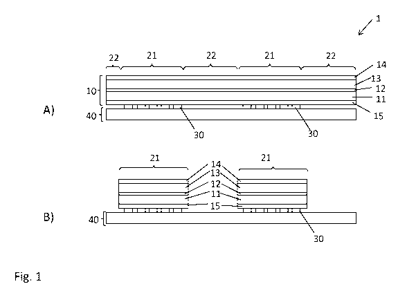
Fig. 1A shows a transfer film 1 with a base film 10 and a further carrier film
40. The
base film 10 comprises a carrier film 11, a detachment layer 12 and a
decorative ply
13, which can comprise a protective varnish layer, a replication varnish
layer, a
reflective layer and an adhesive layer 14.
CA 03007154 2018-06-01
28
A reinforcing layer with a layer thickness of from approx. 0.1 pm to 5 pm,
preferably
from 1 pm to 3 pm can be provided between the replication varnish layer and
the
protective varnish layer for the additional mechanical stabilization in the
case of a
lamination, for example in a plastic card structure.
A primer layer with a layer thickness of from approx. 0.01 pm to 0.5 pm,
preferably
from approx. 0.03 pm to 0.1 pm and/or a further reinforcing layer with a layer
thickness of from approx. 0.1 pm to 10 pm, preferably from approx. 0.5 pm to 5
pm
can also be provided between the reflective layer and the third adhesive layer
(for
io binding to the substrate) for the additional mechanical stabilization in
the case of a
lamination, for example in a plastic card structure.
These above-named reinforcing layers can also be constructed multilayered.
The carrier film 11 is preferably a PET, PEN or BOPP film with a thickness of
from 6
pm to 125 pm. The detachment layer and the decorative ply are now constructed
on
the carrier film 11 successively, by applying further layers. For this, first
the
detachment layer 12 is applied to the carrier film 11. The detachment layer 12
preferably consists of a wax-like material which is softened in particular due
to the
heat arising during a hot-stamping procedure and makes a reliable separation
of the
decorative ply from the carrier film 11 possible. The detachment layer can be
constructed multilayered (for example from a layer of wax and then a layer of
release
varnish). The overall thickness of the detachment layer is preferably between
0.01
pm and 1.2 pm. The protective varnish layer is then applied in a layer
thickness
between 0.5 pm and 1.5 pm. Here it is also possible that the protective
varnish layer
takes on the function of the detachment layer 12 and therefore both makes it
possible
to separate the decorative ply 13 from the carrier film 11 and protects the
decorative
ply 13 against mechanical influences and environmental influences. Here it is
also
possible that the protective varnish layer 13 is colored or contains micro-
and
nanoparticles.
CA 03007154 2018-06-01
29
The replication varnish layer consists of a thermoplastic varnish into which a
surface
structure is molded by means of heat and pressure by the action of a stamping
tool. It
is further also possible that the replication varnish layer is formed by a UV-
crosslinkable varnish and the surface structure is molded into the replication
varnish
layer by means of UV replication.
The replication varnish layer preferably has a layer thickness between 0.5 pm
and 15
pm. The surface structure molded into the replication varnish layer is
preferably a
diffractive surface structure, for example a hologram, Kinegrame or another
grating
io structure with optically diffractive action. Such surface structures
typically have a
spacing of the structural elements in the range of from 0.1 pm to 4 pm. It is
further
also possible that the surface structure is a macroscopic surface structure,
for
example a microlens array or a blazed grating.
After the surface relief has been molded, the reflective layer is applied to
the
replication varnish layer. The reflective layer is preferably a metal layer
made of
chromium, copper, silver or gold or an alloy of such metals, which is vapor-
deposited
under vacuum in a layer thickness of from 0.01 pm to 0.10 pm. It is further
also
possible that the reflective layer 16 is formed by a transparent reflective
layer, for
example a thin or finely structured metallic layer or an HRI (high refractive
index) or
LRI (low refractive index) layer. Such a dielectric reflective layer consists,
for
example, of a vapor-deposited layer made of a metal oxide, metal sulfide,
titanium
dioxide, etc. with a thickness of from 10 nm to 150 nm.
It is further also possible to introduce still further layers instead of or in
addition to the
named layers in the decorative ply 13, which generate an optically variable
effect, for
example a volume hologram layer, a thin-film layer system, a layer of a
crosslinked
cholesteric liquid crystal material or a color layer. It is further also
possible that the
decorative ply comprises one or more electrically conductive or semiconductor
layers, which realize an electrical circuit or an electrical component, for
example an
RF resonant circuit or an RFID tag. This can be for example a metallic layer,
which is
CA 03007154 2018-06-01
either vapor-deposited or printed on and then reinforced by galvanic growth.
In
particular the reflective layer 16 can at the same time serve as an
electrically
conductive layer, which can also be subsequently galvanically reinforced for
this
purpose. The decorative layer 13 can further comprise one or more layers of a
5 magnetic material or an electroluminescent material.
The adhesive layer 14, which can be constructed multilayered and/or on aqueous
or
solvent-containing basis and/or radiation-curing or combinations thereof, is
then
applied in an overall layer thickness of from approximately 0.3 pm to 25 pm.
The
10 adhesive layer 14 preferably consists of a thermally activatable
adhesive and is
applied to the layer 13 over the whole surface, for example by means of a
doctor
blade.
An adhesive layer 15 is applied to the side of the carrier ply 11 facing away
from the
15 decorative ply 13, which adhesive layer preferably also consists of a
thermally
activatable adhesive and is deposited over the whole surface.
As indicated in Fig. 1A and Fig. 1B, the base film 10 and thus also the
decorative ply
13 has two first partial regions 21 and one second partial region 22
surrounding the
20 first partial regions 21. The first partial regions here represent the
part of the
decorative ply which is to be transferred as a security element onto a target
substrate, for example a security document.
The relief structure molded into the replication varnish layer is preferably
selected
25 such that it generates a predetermined optically variable item of
information in the
first partial regions 21. The surface structure molded in the first partial
regions 21
thus preferably differs from the surface structure molded into the replication
varnish
layer in the partial region 22. The reflective layer is further preferably
patterned and
partially provided and provides a second predefined item of information in the
first
30 partial regions 21. The patterned design of the reflective layer in the
first partial
regions 21 thus preferably also differs from that in the second partial region
22. The
CA 03007154 2018-06-01
31
reflective layer is preferably not provided in the second partial region 22.
The optional
further optically active layers of the decorative ply 13 are also preferably
formed
registered relative to the partial regions 21 and provide further items of
information in
the partial regions 21, with the result that the formation of this layer in
the first partial
regions 21 likewise differs from that in the second partial region 22.
It is further also possible that a plurality of first partial regions 21 is
provided, which
are surrounded by a continuous second partial region 22 surrounding the first
partial
regions 21.
A first adhesive layer 30 is applied to the further carrier film 40. The
adhesive layer
30 here is applied only in the region of the first partial regions 21 and
preferably in a
grid.
The adhesive layer 30 is a UV-activatable adhesive. The adhesive which can be
used for the adhesive layer 30 has the following composition, for example:
Dicyclopentyloxyethyl methacrylate 50% to 60%
2-Hydroxyethyl methacrylate 8%
Trimethylolpropane triacrylate 40% to 30%
(3-(2,3-Epoxypropoxy) propyl)trimethoxysilane 1%
1-Hydroxy-cyclohexyl- phenyl-ketone
(lrgacure 184 (BASF)) 1% to 2%
By way of example, a different composition adhesive which can be used for the
adhesive layer 30 is, for example:
Dicyclopentyloxyethyl methacrylate 50% to 55%
2-Hydroxyethyl methacrylate 8%
Trimethylolpropane triacrylate 35% to 30%
Phenol, ethoxylated, esters with acrylic acid 5%
CA 03007154 2018-06-01
32
Dipropylene glycol diacrylate 5%
(3-(2,3-Epoxypropoxy) propyl)trimethoxysilane 1%
1-Hydroxy-cyclohexyl-phenyl-ketone
(lrgacure 184 (BASF)) 1% to 2%
The adhesive layer 30 is applied to the carrier film 40 in a layer thickness
of from 0.1
pm to 10 pm by means of a printing process, by means of pouring or by means of
a
doctor blade.
The carrier film 40 is a transparent plastic film, which preferably consists
of PET,
PVC, PEN or BOPP film and has a layer thickness of from 6 pm to 250 pm.
The production of the transfer film 1 is illustrated in steps in Figures 2 and
3. As Fig.
2A shows, the base film 10 is initially prepared without the adhesive layers
14 and
15, which are applied in the following method step. After an optional drying
of the
adhesive layers 14 and 15 has been carried out, the transfer film 40 is
connected to
the base film via the adhesive layer 30. The adhesive layer 30 can be applied
to the
transfer film 40 or to the adhesive layer 15. It is possible and preferred to
apply the
adhesive layer 30 only in the region 21.
Alternatively the adhesive layer 30 can also be applied over the whole surface
and
only activated in the region 21. A first region of the adhesive layer 30
activated by
exposure. For this the film structure shown in Fig. 2C, consisting of the
carrier film 40,
the adhesive layer 30, the carrier film 11, the detachment layer 12 and the
decorative
ply 13, is exposed to UV light in the region 31. For this a collimated light
source is
used, which is on the side of the carrier film 40 facing away from the carrier
film 11
and is spaced apart from the carrier film 40. Here an exposure mask, which
masks
the region 32 and thus makes a selective exposure of the region 31 possible,
is
arranged in the beam path between the light source and the adhesive layer 30.
The
exposure light source and the exposure mask are preferably part of a drum
imagesetter, over which the film body is guided. The exposure mask here is
formed
CA 03007154 2018-06-01
33
and arranged such that the region 31 largely covers the first partial regions
21 and is
positioned relative to the first partial regions 21 within the framework of a
register
tolerance of from preferably 0.1 mm to 2.0 mm.
In the region 32, the adhesive layer 30 is not exposed by UV light and is thus
not
activated.
The combination of an adhesive of the type shown in the above tables
(deposition by
means of flexographic printing with a grid density between 40% and 80% with 40
to
60 lines per cm) for the adhesive layer 30 and a heat-sealable adhesive, which
has
been deposited between 2 g/m2 and 4 g/m2, for the adhesive layer 15 has proved
to
be particularly successful. The UV adhesive is preferably purely radically UV-
curing
and therefore has a solids content of 100%. A monomer fraction can likewise
evaporate during the UV curing, because heat is also introduced into the layer
due to
the UV radiation, if the adhesive is not completely enclosed between two
neighboring
layers, in particular films.
The heat-sealable adhesive consists of acrylates and solvent (isopropanol +
toluene).
The solids content is 19% to 20% in order to guarantee the deposition using
the
varnishing machine. At ambient temperature (approx. 20 C) after drying it has
a non-
tacky surface, in particular at room temperature, as neither the melting point
nor the
glass transition temperature is below 30 C and thus they are always above the
processing (production) temperature of the film.
In a further step illustrated in Fig. 3, the decorative ply 13, the detachment
layer 12
and the carrier film 11 are severed along the boundary lines defining the
first partial
regions 21 and separating the first partial regions 21 from the partial region
22.
These layers are preferably severed by means of a punch, which introduces
corresponding recesses into the film body consisting of the layers 30 as well
as 15 to
11. Here it is also possible that the punch depth is selected such that the
carrier film
is also partially severed. It is further also possible that the carrier film
11 is not
CA 03007154 2018-06-01
34
completely, but only partially severed. This can on the one hand occur in such
a way
that regions in which the carrier film 11 is completely severed and is not
severed
alternate along the boundary line or that the carrier film 11 is not severed
over its
entire thickness, but only for example over 80% of its thickness.
In a further step shown in Fig. 3B, the part of the base film 10 (a "grating")
comprising
the partial region 22 is removed from the carrier film 40, wherein because of
the
adhesive layer 30 activated in the region 31 the base film remains adhering to
the
carrier film 40 in the first partial regions 21 and remains on the carrier
film 40. After
io the "grating" has been removed, the multilayer body 1 shown in Fig. 3C,
which can
be used as a security element or as a transfer film for the application of a
security
element to a target substrate, thus results.
As illustrated with the aid of Fig. 4, the multilayer body 1 can be used as a
transfer
film for the application of a security element 23 to a target substrate 70.
For this the
multilayer body 1 is placed on the target substrate 70, and the adhesive
layers 14
and 15 are activated in a first partial region by a correspondingly shaped hot-
stamping die 71. By the activation of the adhesive layer 14 the transfer ply
of the
multilayer body 1 is connected to the target substrate 70. At the same time an
activation of the adhesive layer 15 is effected, by which the adhesion between
the
carrier plies 11 and 40 is increased, preferably by more than 50%, preferably
more
than 100%, particularly preferably more than 200%.
The stamping is effected at a temperature of from 80 C to 300 C, preferably
from
1 00 C to 240 C, particularly preferably from 100 C to 180 C and/or with a
stamping
pressure of from 10 N/cm2 to 10,000 N/cm2, preferably from 100 N/cm2 to 5000
N/cm2 and/or with a stamping time of from 0.01s to 2s.
The multilayer body comprising the carrier film 40, the adhesive layer 30 and
the
carrier film 11 is then removed from the applied region of the decorative ply
13, with
the result that the security element 23 remains on the target substrate 70, as
is
CA 03007154 2018-06-01
shown in Fig. 4. By the activation of the adhesive layer 15 it is ensured that
no carrier
film remains on the security element 23.
Alternative structures of the decorative ply 13 are illustrated in Figs. 5 and
6. The
5 further layers as well as the processing, however, correspond to the
embodiment
already described.
In the variant of the transfer film 1 according to Fig. 5, the decorative ply
comprises
an optional protective varnish layer 131 with a preferred layer thickness of
from 0.1
10 pm to 20 pm, particularly preferably from 0.5 pm to 10 pm, a replication
varnish layer
with a preferred layer thickness of from 0.1 pm to 10 pm, particularly
preferably from
0.5 pm to 5 pm with reflective layer 132, a primer varnish layer 133 with a
preferred
layer thickness of from 0.1 pm to 5 pm, particularly preferably from 1 pm to
3v, a
volume hologram layer 134 with a preferred layer thickness of from 5 pm to 50
pm,
15 particularly preferably from 10 pm to 20 pm and a sealing varnish layer
135 with a
preferred layer thickness of from 0.1 pm to 5 pm, particularly preferably from
5 pm to
15 pm. A volume hologram is inscribed into the volume hologram layer 134,
which
forms the essential security feature of the resulting security element 32.
20 In the variant according to Fig. 6, the decorative ply 13 consists of a
print promoter
layer 136 with a preferred layer thickness of from 1 pm to 30 pm, particularly
preferably from 1 pm to 3 pm, to which an individualization feature can be
applied by
inkjet printing. This layer 136 can also be combined with all further layers
of the
decorative ply 13 already described in order thus to create an individualized
security
25 element 23.
A schematic sectional representation of a further transfer film 1 is shown in
Figures
7A and 7B. As is shown in Figure 7A, a detachment system 17 is provided on the
second carrier film 40. The detachment system 17 makes it possible for the
first
30 carrier film 11 to remain on the security element 23 or in the layer
composite thereof
during the application of the security element 23.
CA 03007154 2018-06-01
36
By also applying the first carrier film 11 a self-supporting security element
23 can be
produced, which can seal or cover for example apertures, in particular window
openings, in the target substrate 70. The additional mechanical stability
which the
first carrier film 11 gives the security element 23 can furthermore serve to
increase
the optical brilliance of the security element 23 when the security element 23
is for
example laminated into a plastic composite, as can be the case for example
with
security documents made of polycarbonate (PC) in an ID card format or other
laminates. This additional mechanical stability can also be advantageous in
the
io further processing of the target substrate 70, for example in the case
of overprinting
with die stamping. The arrow shown in Figure 7A shows the position of the
separation during application of the transfer film 1 to a target substrate 70.
The base
film 10 here is preferably formed as a laminating film.
The overall thickness of the detachment system 17 is preferably between 0.01
pm
and 4 pm. The detachment system 17 preferably has a layer made of wax 171. The
wax-like material is softened due to the heat arising during a hot-stamping
procedure
and makes a reliable separation of the second carrier film 40 possible.
As shown in Figures 7A and 7B, the detachment system 17 can furthermore have a
layer made of a varnish 172. The varnishes 172 are preferably based on
acrylates,
polyurethanes or cellulose derivatives.
The varnish layer 172 preferably has a thickness in the range of from 0.1 to 3
pm,
preferably in the range of from 0.2 to 1.5 pm.
Figure 8 shows a possible production of the transfer film 1. Here the
detachment
system 17, in particular consisting of a wax layer 171, which adjoins the
second
carrier film 40, and a varnish layer 172, is applied to the second carrier ply
40. The
base film 10 preferably has the adhesive layer 14, the decorative ply 13 as
well as
the first carrier film 11 and the adhesive layer 15.
CA 03007154 2018-06-01
37
Figure 9 shows the application, at least in regions, of the transfer film 1 to
a target
substrate 70. For this the transfer film 1 is placed on the target substrate
70 and the
adhesive layers 14 and 15 are activated in a first partial region 21 by a
correspondingly shaped hot-stamping die 71. By the activation of the adhesive
layer
14 the transfer ply of the transfer film 1 is joined to the target substrate
70. At the
same time an activation of the adhesive layer 15 is effected, by which the
adhesion
between the first carrier ply 11 and the detachment system 17 is increased.
The wax
layer 171 softening due to the action of heat during the application
furthermore
lo ensures a clean separation between the detachment system 17 and the
second
carrier film 40.
As shown in Figure 9, the detachment system 17 remains on the target substrate
70
after application together with the first carrier film 11 and the decorative
ply 13,
is preferably as a security element 23. Because the detachment system 17
forms the
outer surface of the security element 23 and can be designed in various
different
ways, the security element can hereby be provided with additional functions.
Examples are a better wettability or overprintability with further functional
layers or,
conversely, a hydrophobic function or functions to repel other liquids or also
the
20 generation of optical matting and/or of an optical gloss and/or the
generation of
particular tactile properties. It is also possible to add additional security
prints in the
visible wavelength range, UV range or IR range. Individual or all layers of
the
detachment layer system can be provided over the whole surface or only in
partial
surface regions.
A schematic sectional representation of a further transfer film 1 is shown in
Figures
10A and 10B. As is shown in Figure 10A, a detachment system 17 is provided on
the
first carrier film 11. The detachment system 17 makes it possible for the
first carrier
film 11 to remain on the security element 23 or in the layer composite thereof
during
the application of the security element 23.
CA 03007154 2018-06-01
38
A self-supporting security element 23 can hereby be produced, which can seal
or
cover for example apertures, in particular window openings, in the target
substrate
70. The additional mechanical stability which the first carrier film 11 gives
the security
element 23 can furthermore serve to increase the optical brilliance of the
security
element 23 when the security element 23 is for example laminated into a
plastic
composite, as can be the case for example with security documents made of
polycarbonate (PC) in an ID card format or other laminates. This additional
mechanical stability can also be advantageous in the further processing of the
target
substrate 70, for example in the case of overprinting with die stamping.
The arrow shown in Figure 10A shows the position of the separation during
application of the transfer film 1 to a target substrate 70. The base film 10
here is
preferably formed as a laminating film.
The overall thickness of the detachment system 17 is preferably between 0.01
pm
and 4 pm. The detachment system 17 preferably has a layer made of wax 171. The
wax-like material is softened due to the heat arising during a hot-stamping
procedure
and makes a reliable separation of the second carrier film 40 possible.
As shown in Figures 10A and 10B, the detachment system 17 can furthermore have
a layer made of a varnish 172. The varnish 172 is preferably based on
acrylates,
polyurethanes or cellulose derivatives.
The varnish layer 172 preferably has a thickness in the range of from 0.1 to 3
pm,
preferably in the range of from 0.2 to 1.5 pm.
Figure 11 shows a possible production of the transfer film 1. Here the
detachment
system 17 is applied to the side of the first carrier film 11 of the base film
10 facing
away from the decorative ply 13. The detachment system 17 can have a wax layer
171 and a varnish layer 172. Furthermore, the adhesive layer 15 is then
preferably
applied to the outer, free side of the detachment system 17. In the further
processing,
CA 03007154 2018-06-01
39
the adhesive layer 15 is preferably in contact with the adhesive layer 30.
This
embodiment variant can also make it possible for the base film 10 to remain on
the
security element 23 or in the layer composite thereof during the application
of the
security element 23. A self-supporting security element 23 can thereby be
produced,
which can seal or cover for example apertures, in particular window openings,
in the
target substrate.
It is also conceivable that, before the detachment system 17 is applied, one
or more
auxiliary layers (not shown) are applied to the side of the first carrier film
11 of the
base film 10 facing away from the decorative ply 13 and are then therefore
arranged
between the first carrier film 11 and the detachment system 17. It is hereby
possible
with the aid of these auxiliary layers to provide the outer surface of the
security
element 23 with additional functions. Examples are better wettability or
overprintability with further functional layers or, conversely, a hydrophobic
function or
functions to repel other liquids or also the generation of optical matting
and/or of an
optical gloss and/or the generation of particular tactile properties. It is
also possible to
add additional security prints in the visible wavelength range, UV range or IR
range.
A further function can consist of increasing the adhesive bond to further
cover plies
when the target substrate 70 is laminated into a document or a document
composite.
Individual or all layers of the detachment layer system can be provided over
the
whole surface or only in partial surface regions.
Figure 12 shows the application, at least in regions, of the transfer film 1
to a target
substrate 70. For this the transfer film 1 is placed on the target substrate
70. By the
activation of the adhesive layer 14 the transfer ply of the transfer film 1 is
joined to
the target substrate 70. The wax layer 171 softening due to the action of heat
during
the application ensures a clean separation between the detachment system 17
and
the first carrier film 11.
As shown in Figure 12, the detachment system 17 is detached from the security
element 23 after application to the target substrate 70. If auxiliary layers
are arranged
CA 03007154 2018-06-01
between the detachment system 17 and the first carrier film 11, the auxiliary
layers
form the outer, free surface of the security element 23. If these auxiliary
layers are
dispensed with, the carrier film 11 forms the outer, free surface of the
security
element 23 and thus enables a particularly brilliant optical effect of the
security
5 element 23.
CA 03007154 2018-06-01
41
List of reference numbers
1 transfer film
base film
5 11 carrier film (of the base film)
12 detachment layer (of the base film)
13 decorative ply (of the base film)
131 protective varnish layer (of the base film)
132 replication varnish layer (of the base film)
to 133 primer varnish layer (of the base film)
134 volume hologram layer (of the base film)
135 sealing varnish layer (of the base film)
136 print promoter layer (of the base film)
14 adhesive layer (of the base film)
15 adhesive layer (of the base film)
16 reflective layer (of the base film)
17 detachment system
171 wax layer
172 varnish layer
21 first partial region
22 second partial region
23 security element
adhesive layer
31 region
25 32 region
second carrier film
70 target substrate
71 hot-stamping die