Note : Les descriptions sont présentées dans la langue officielle dans laquelle elles ont été soumises.
CA 03010394 2018-06-29
Kehl, Ascher], Liebhoff & Ettmayr 12 December
2016
Patent Attorneys ¨ Partnership Our Ref.:
5015-60-PCT
METHOD AND DEVICE FOR PLANAR CREATION OF MODIFICATIONS IN SOLID
STATES
The present invention is in the field of solid-state disk production, i.e.,
wafer production.
According to claim 1, the present invention relates to a method for creating
modifications in a
solid state and according to claim 10 it relates to a device for creating
modifications in a solid
state.
The cold split method (cf. W02010072675) is a novel method for cutting
semiconductor disks
(wafers) out of ingots, i.e., boules (semiconductor ingots, depending on the
production
method ¨ drawing from a melt or vapor deposition from a gas phase). In the
cold split
method, a laser-damage layer is applied as the intended breaking point in the
desired depth
through the front face of the semiconductor ingot. A proprietary polymer film
having good
adhesion is applied and cooled drastically. A semiconductor wafer is formed
from the ingot or
boule by detachment because of the mechanical stresses caused by the great
difference in
thermal expansion coefficients.
This is an alternative to traditional cutting of wafers using inner diameter
saws or guided
wires (diamond-tipped or grinding suspension/slurry). These methods result in
a variance in
thickness due to wandering of the wires while the wafers are being sliced. As
a result of this
variation in thickness, the wafers show bulging and bending. Semiconductor
manufacturers
as further processors of these wafers have accepted these deviations in
planarity only to a
certain extent. For this reason, after being split off, the semiconductor
wafers must be
processed by a series of surface treatments. These are done by adjusting the
planarity,
parallelism and roughness by means of etching, lapping and chemicomechanical
polishing
steps.
Deviations in surface properties may also occur in the cold split method.
These deviations
can be removed from the wafer as well as from the ingot by planarization and
polishing steps
that follow the cold split method.
For wafers, a planar split means less reserve in planarization slicing, which
further increases
the overall material efficiency of the cold split method in comparison with
traditional wafering
1
CA 03010394 2018-06-29
Kehl, Ascherl, Liebhoff & Ettmayr 12 December
2016
Patent Attorneys ¨ Partnership Our Ref.:
5015-60-PCT
methods. The total material efficiency is given by the ratio of the wafer
thickness used, i.e.,
the number of defect-free wafers having the final dimension (e.g., 23 wafers
of 350 pm
thickness = effective thickness 8050 pm) to the initial thickness of the
semiconductor ingot
(ingot or boule, e.g., 25,000 pm). In this example using a planar laser-
modified cold split
process, the wafer yield can be increased to 84% versus <40% with the
traditional wafering.
Planarity must be restored in the remaining semiconductor ingot before the
next lasering
operation because otherwise the deviations would propagate throughout the
remaining
process and might even increase. This increase occurs due to different optical
path lengths
in materials with a very high refractive index optically (e.g. Si: n = 3.6;
SiC: n = 2.6).
Therefore, if the distance from the laser head to the surface fluctuates, then
the laser beam
will also pass through different optical optical paths of different refractive
indices and different
path lengths up to the focus. An error of 1 pm in the distance to the surface
thus causes an
n-fold error within the material.
To achieve a very high planarity of the laser plane, deviations in the pm
range are allowed
over the length of the wafer, but it is difficult to achieve such deviations
with mechanical
wedge compensation, which can be achieved only to a limited extent with
autofocus alone.
In automatic mask exposure systems, for example, which work with distance
lighting
(proximity photolithography), mechanical wedge compensation in the pm range is
state of the
art. However, only extremely planar masks and substrates are statically
compensated here
because the sample does not move in a highly dynamic manner with respect to
the
processing lens. Only static applications can be implemented by using
mechanical wedge
compensation and only correction planes (biaxial tilting) can be compensated.
The traditional autofocus maintains a constant distance from the processing
lens to the
surface. It is also possible in this way to maintain tracking in the laser
microprocessing of
surfaces in the pm range. In surface processing, the laser naturally runs only
through a
medium (usually air) up to the focus point. The traditional autofocus has the
disadvantage
that only tracking of the surface profile is possible. Furthermore, the
profile is magnified by
the factor of the substrate refractive index, and finally, planarization is
impossible.
2
CA 03010394 2018-06-29
Kehl, Ascherl, Liebhoff & Ettmayr 12 December
2016
Patent Attorneys ¨ Partnership Our Ref.:
5015-60-PCT
Furthermore, in addition to mechanical wedge compensation and traditional
autofocus,
another known method is 3D photolithography with multiphoton absorption and
planarization
prior to lasering.
The 3D photolithography method with multiphoton absorption greatly resembles
laser
modification in volume because the focus point here is manipulated in the
processing volume
while the surrounding material remains unmodified. These processes work with
liquid
photoresists and therefore yield a surface that is flat and smooth (surface
tension, water
balance principle). The lens here is manipulated directly in the resist
(immersion) and
therefore does not undergo any spreading in different media. This method is
not
advantageous because a system having only a homogenous medium/without an
interface is
available.
Furthermore, there are planarization and polishing methods, which can produce
planarity and
roughness of almost any quality. However, the equipment complexity and,
associated
therewith, the processing costs fluctuate greatly. This method is a
disadvantage because an
additional reserve of material is required in order to achieve a lower yield
or overall material
efficiency, which results in increased process costs. Furthermore, there is no
saving in terms
of the autofocus because placement errors can still be corrected anyway.
The object of the present invention is thus to provide a method and a device
which will permit
a very precise creation of modifications in the interior of the solid states,
even in the case of
particularly large solid states having a diameter of more than 6 inches. The
solid-state
components and/or strata removed from a solid state by means of crack
propagation should
preferably result in less effort with regard to reworking, i.e., at a distance
from the surface of
the solid state.
The aforementioned object is achieved according to the present invention by a
method
according to claim 1. The method according to the invention serves to create
modifications in
the solid state, wherein a crack guidance region for guiding a crack for
separation of a solid-
state component, in particular a solid-state layer from the solid state is
predetermined by the
modifications. The method according to the invention preferably includes at
least these
steps: moving the solid state relative to a laser processing system, then
creating and/or
successive emission of a plurality of laser beams by means of the laser
processing system
3
CA 03010394 2018-06-29
Kehl, Ascher!, Liebhoff & Ettmayr 12 December
2016
Patent Attorneys ¨ Partnership Our Ref.:
5015-60-PCT
for creating at least one modification within a solid state, wherein the laser
processing
system (8) is adjusted continuously as a function of at least one parameter
and preferably as
a function of a plurality of parameters, in particular at least two
parameters, for defined
focusing of the laser beams and/or for adaptation of the laser energy.
This approach is advantageous because it provides a method in which the focus
within the
material does not directly track the surface but instead is provided with
corrections. If these
deviations are to be detected in real time, then a simple provision with
correction factors can
be performed. The correction factors here preferably correspond to the
parameters used to
adjust the laser processing system.
The position of the focus within a material is also a function of the
refractive index and the
depth of processing (imaging errors depend on the material).
The method according to the invention can preferably also be understood as a
novel control
method for focus tracking as a real-time system.
The adjustment of the laser processing system preferably takes place by means
of an
algorithm executed by a control system, in particular for differentiating
substrate tilting due to
placement errors (tilting with respect to the machine holders) and/or
planarity errors in the
semiconductor ingot.
Within the scope of the present invention, a modification is understood to be
a change in the
lattice structure of the solid state. In particular the change in the lattice
structure takes place
due to multiphoton excitation.
Additional preferred embodiments of the present invention are the subject
matter of the
dependent claims and/or of the following parts of the description:
According to a preferred embodiment of the present invention, a first
parameter is the
average refractive index of the material of the solid state or the refractive
index of the
material of the solid state is in the region of the solid state that is to be
traversed by the laser
beams to create a defined modification, and a second parameter is the depth of
processing
in the region of the solid state that is to be traversed by the laser beams to
create a defined
4
CA 03010394 2018-06-29
Kehl, Ascherl, Liebhoff & Ettmayr 12 December
2016
Patent Attorneys ¨ Partnership Our Ref.:
5015-60-PCT
modification. This embodiment is advantageous because the processing depth and
the
refractive index are parameters that have substantial effects on the precision
of the focus
point thereby created.
According to another preferred embodiment, an additional or alternative
parameter is the
degree of doping of the solid-state material, which is preferably determined
by analysis of
backscattered light (preferably Raman scattering), wherein the backscattered
light has a
different wavelength or a different wavelength range than the incident light
defined for
triggering the backscattering, such that a Raman instrument is a component of
the device,
and the degree of doping is determined by means of the Raman instrument, such
that one or
more or all of these parameters are preferably detected by means of a shared
detection
head, in particular being detected simultaneously. Raman spectroscopy is
preferably also
used on glass, sapphire and aluminum oxide ceramics. The Raman method is
advantageous
because it performs measurements in the depth of a material but only from one
side, does
not require a high transmittance and outputs the charge carrier
density/doping, which can be
correlated with the laser parameters, by means of a fit to the Raman spectrum.
The first parameter is determined by means of a refractive index determination
means, in
particular by means of spectral reflection according to another preferred
embodiment of the
present invention and/or the second parameter is determined by a topography
determination
means, in particular by a confocal-chromatic distance sensor.
Data on the parameters, in particular the first parameter and the second
parameter, is
provided in a data memory device according to another preferred embodiment of
the present
invention and is sent to a control system at least before creation of the
modifications, wherein
the control system adjusts the laser processing system as a function of the
respective
location of the modification to be created. In particular the fluctuations in
the refractive index
over the semiconductor ingot are not always highly resolved or detectable
rapidly enough for
real-time control purposes. Therefore, focus guidance with prior knowledge is
required. The
prior knowledge is represented here by the data on the parameters detected
and/or
determined and/or generated before the processing and/or creation of the
modification.
According to another preferred embodiment of the present invention, the
control system for
adjusting the laser processing system also processes distance data to yield a
distance
CA 03010394 2018-06-29
Kehl, Ascher!, Liebhoff & Ettmayr 12 December
2016
Patent Attorneys ¨ Partnership Our Ref.:
5015-60-PCT
parameter, wherein the distance parameter represents the distance of the
respective
location, at which laser beams can be initiated for generating the respective
modification in
the solid state at the point in time of creation of the modification with
respect to the laser
processing system, wherein the distance data is detected by means of a sensor
device. This
embodiment is advantageous because rapid real-time control with the distance
sensor and
adjustable correction factors can be supplemented by location-dependent
control of the
correction factors.
According to another preferred embodiment of the present invention, the laser
processing
system is adjusted by a sensor means, in particular a refractive index
determination means
and a topography determination means, as a function of a determination of the
first
parameter and the second parameter during the creation of the modification.
According to another preferred embodiment of the present invention, the solid
state is
arranged on a receiving device, wherein the receiving device can be moved in
X/Y direction
or rotated about an axis of rotation, such that the rate of rotation of the
receiving device can
be varied by means of a drive device as a function of the distance of the
location at which the
laser beams can penetrate into the solid state from the axis of rotation,
preferably increasing
with a decrease in the distance from that location, or wherein the receiving
device can rotate
about the axis of rotation at more than 100 revolutions per minute, preferably
at more than
1000 revolutions per minute and especially preferably at more than 1500
revolutions per
minute, and laser beams can be emitted by the laser processing system at a
frequency of at
least 0.5 MHz, preferably of at least 1 MHz, and especially preferably of at
least 5 MHz or
MHz for generating the modifications.
According to another preferred embodiment of the present invention, the laser
beams
penetrate into the solid state over a surface area of the portion of the solid
state to be
removed, wherein the portion of the solid state to be removed has a smaller
average
thickness than the remaining solid state.
According to another preferred embodiment of the present invention, an
additional or
alternative parameter is the degree of doping of the solid state at a
predetermined location or
in a predetermined region, in particular in the interior of the solid state,
in particular at a
distance from the solid-state surface. The degree of doping is preferably
linked to location
6
CA 03010394 2018-06-29
Kehl, Ascherl, Liebhoff & Ettmayr 12 December
2016
Patent Attorneys ¨ Partnership Our Ref.:
5015-60-PCT
information, such that a therapeutic map is generated and/or spatially
resolved treatment
instructions are provided, which predetermine the laser parameters, in
particular the laser
focus and/or laser energy and/or other machine parameters, in particular the
rate of advance
as a function of the location.
According to another preferred embodiment of the present invention, the degree
of doping is
determined by analysis of backscattered light within elastic scattering (Raman
scattering)
wherein the backscattered light has a different wavelength or a different
wavelength range
than incident light defined for triggering the backscattering, wherein the
backscattered light is
backscattered from the predefined location or from the predetermined region.
This embodiment is advantageous because the process must be guided in a
locally adapted
manner in the laser method, in particular on SIC (but also other materials)
(for example, a
different laser energy, etc.). It has been recognized according to the
invention that in the
case of SIC, for example, the doping in particular is crucial here because
this alters the
transparency of the material for the processing wavelength and necessitates
higher laser
energies.
According to another preferred embodiment of the present invention, the degree
of doping is
determined by ellipsometric measurement (for example, Muller matrix
ellipsometry with rear
side reflection). The ellipsometric measurement is preferably based on optical
transmission
of the material.
According to another preferred embodiment of the present invention, the degree
of doping is
determined by a transmission measurement that is calibrated purely optically,
wherein the
calibration is performed by a Hall measurement and a 4-point measurement. This
method is
also capable of determining the doping/number of free charge carriers in the
material, which
then makes it possible to determine the laser energy required for the process.
According to another preferred embodiment of the present invention, the degree
of doping is
determined by means of an eddy current measurement, wherein differences in
conductivity in
the solid-state material are preferably determined and evaluated.
7
CA 03010394 2018-06-29
Kehl, Ascher!, Liebhoff & Ettmayr 12 December
2016
Patent Attorneys ¨ Partnership Our Ref.:
5015-60-PCT
In eddy current measurements and/or when using eddy current sensors and/or
eddy current
measurement technology, a transceiver coil is preferably used to detect local
differences in
conductivity. A high-frequency primary electromagnetic alternating field is
generated in the
transmission coil. Then eddy currents (currents flowing locally) are induced
in the conductive
material, and these in turn induce a secondary electromagnetic alternating
field directed in
the opposite direction. The superpositioning of these fields can be measured,
separated and
analyzed. Various quality features (layer thickness, layer resistance,
homogeneity of the
material) of mainly thin conductive layers but also of bulk material can be
measured in this
way. In the transmission arrangement (test body between the transceiver coil),
optimum
approaches are achieved, but an arrangement of the two coils on one side of
the sample is
also possible for reflection measurements. Different depths of penetration and
sensitivities
can be utilized thanks to the adapted design of the coils and the choice of
frequency.
Therefore there are fundamentally several measurement methods with which the
doping can
be measured in principle. A rapid, non-contact and non-destructive method is
important here.
Furthermore, the present invention relates to a method for separating at least
one solid-state
layer from a solid state. The method according to the invention comprises at
least one of
claims 1 through 8. Furthermore, the method according to the invention
comprises the
creation of so many modifications in the solid state that the solid-state
layer becomes
detached due to the modification created, or the method according to the
invention
comprises the steps of arranging or creating a receiving layer on the solid
state, wherein the
receiving layer comprises, contains or consists of a polymer material, in
particular
polydimethylsiloxane or an elastonner or an epoxy resin or a combination
thereof, and the
polymer material undergoes a glass transition due to thermal exposure of the
receiving layer
for creation of crack propagation stresses in the solid state, in particular
mechanical stresses,
wherein a crack propagates in the solid state along the crack guidance region
due to the
crack propagation stresses.
According to another preferred embodiment of the present invention, the
receiving layer
comprises or consists at least mostly and preferably completely of a polymer
material, based
on weight, wherein the glass transition of the polymer material occurs between
-100 C and
0 C, in particular between -85 C and -10 C or between -80 C and -20 C or
between -65 C
and -40 C or between -60 C and -50 C.
8
CA 03010394 2018-06-29
Kehl, Ascherl, Liebhoff & Ettmayr 12 December
2016
Patent Attorneys ¨ Partnership Our Ref.:
5015-60-PCT
The receiving layer preferably contains or consists of a polymer-hybrid
material, which
especially preferably forms a polymer matrix, wherein the polymer matrix
contains a filler,
such that the polymer matrix is preferably a polydimethylsiloxane matrix and
the amount by
weight of the polymer matrix in the polymer-hybrid material preferably amounts
to 80% to
99% and especially preferably 90% to 99%. The receiving layer is preferably
supplied as a
prefabricated film and is connected to the solid state, in particular by
adhesion or bonding.
Therefore, according to the invention a polymer-hybrid material is provided
for use in a
splitting method, in which at least two solid-state pieces are created from a
solid-state
starting material. The polymer-hybrid material according to the invention
comprises a
polymer matrix and at least one first filler embedded therein. Inasmuch as the
following
discussion relates to a/the filler, the possibility of a plurality of fillers
should also be taken into
account at the same time. For example, the filler may comprise a mixture of
different
materials, for example, metal particles and inorganic fibers.
Any polymer or a blend of different polymers may be used as the polymer matrix
as long as
the stresses required for dividing the solid-state starting material can be
created with the help
of these polymers. For example, the polymer matrix may be embodied as an
elastomer
matrix, preferably as a polydiorganosiloxane matrix, especially preferably as
a
polydimethylsiloxane matrix. Such polymer materials can be used especially
easily as the
matrix material in combination with fillers because the properties are
adjusted in a flexible
manner based on the variable degree of crosslinking and can be adapted to the
respective
filler and to the solid-state starting material that is to be divided.
According to one
embodiment variant, the amount by weight of the polymer matrix and the polymer-
hybrid
material is 80% to 99%, preferably 90% to 99%.
The first filler may be of an organic or inorganic nature and may consist of a
chemical
element as well as a chemical compound or a substance mixture, for example, an
alloy.
The first filler is designed so that it acts as a reactant, initiator,
catalyst or promoter during
separation of the polymer-hybrid material from the solid-state piece after
division and
therefore results in a more rapid separation of the polymer-hybrid material
from the solid-
state piece after being divided in comparison with a polymer material without
the first filler.
9
CA 03010394 2018-06-29
Kehl, Ascher!, Liebhoff & Ettmayr 12 December
2016
Patent Attorneys ¨ Partnership Our Ref.:
5015-60-PCT
The specific chemical composition and embodiment of the first filler as well
as its amount by
weight depend in particular on the specific material of the polymer matrix,
which is to be
separated, the solvent used for this purpose and the reactants used. In
addition, the material
of the solid-state starting material and the dimensions of the solid-state
starting material to be
divided also play a role.
The specific amount of the first filler in the polymer matrix depends greatly
on the material of
the filler and its mechanism of action. Firstly, the polymer matrix must be
able to do justice to
its object of creating stresses, despite the presence of the filler. Secondly,
the amount of the
first filler must be great enough to achieve the desired influence on the
removal of the
polymer. Those skilled in the art can determine the optimum amount by weight
of the first
filler within the scope of simple experiments conducted as a function of
concentration.
To improve the mechanical properties, an additional filler, for example,
pyrogenic silica in the
form of an inorganic network in the polymer, can also contribute toward an
improvement in
the mechanical properties. In addition to these strong interactions in the
form of the network,
weaker interactions can also contribute to the improvement through purely
hydrodynamic
reinforcement. For example, a targeted increase in viscosity can be mentioned
here,
permitting improved processing in the splitting method and thus possibly
contributing toward
improved manufacturing tolerances. In addition, through this interaction, a
reduction in the
internal degrees of freedom with regard to a structural reorientation is made
more difficult
with an increase in the reinforcement.
This results in the desired reduction in the glass transition temperature of
the polymer used
in the polymer-hybrid material, which allows the advantage of a lower
temperature in the
splitting method. According to the invention, the first filler in a polymer-
hybrid material is used
to accelerate the release of the polymer-hybrid material from a solid-state
piece which is
obtained by division by means of a splitting method, in which a solid-state
starting material is
divided into at least two solid-state pieces.
The first filler may be distributed in the polymer matrix in such a way that
the amount by
weight of the first filler starting from the outer, i.e., lower, interface of
the polymer-hybrid
material, which is joined to the solid-state starting material during the
splitting process
CA 03010394 2018-06-29
Kehl, Ascherl, Liebhoff & Ettmayr 12 December
2016
Patent Attorneys ¨ Partnership Our Ref.:
5015-60-PCT
decreases in the direction of another interface in the polymer-hybrid material
that is arranged
in parallel with the lower interface. This means that the amount by weight of
the filler is
greater near the solid-state starting material and/or piece than in the other
regions of the
polymer-hybrid material. This distribution of the first filler permits
particularly effective
removal of the polymer-hybrid material after separation because the first
filler is close to the
interface to the solid-state piece and can manifest its effect there. At the
same time, the
remaining regions of the polymer-hybrid material have fewer or no parts at all
of the first filler,
so that the function of the polymers is influenced as little as possible.
In one embodiment, the polymer-hybrid material has a layered structure,
wherein only one
layer facing the solid-state starting material contains the first filjer,
while the remaining
polymer-hybrid material is free of the first filler.
In addition, a lower region of the polymer-hybrid material, which is directly
adjacent to its
lower interface, may be free of the first filler. This may result in a
sequence of regions as
follows: next to the solid-state starting material, there is first a region
without the first filler,
followed by a region with a large amount of the first filler and then a region
with a small
amount of the first filler or without any of the first filler.
These regions and all the regions described below may be embodied in the form
of layers,
i.e., the region extends primarily parallel to the interlace of the solid-
state starting material to
which the polymer-hybrid material is applied and has a longitudinal and
transverse extent, at
least in the region of this interface.
A lower region without the first filler may be provided in particular for the
case when the first
filler has a negative effect on the adhesion of the polymer-hybrid material to
the solid-state
starting material. To prevent this, a region without the first filler is
arranged first, followed by a
region with a large amount of the first filler, so that the first filler can
fulfill its function. A lower
layer without the first filler may have a thickness between 10 pm and 500 pm,
for example,
100 pm.
In addition, an upper region of the polymer-hybrid material, which is directly
adjacent to its
upper interface, may be free of the first filler. The upper interface is
understood to be the
interface bordering the polymer-hybrid material on the opposite side from the
lower interface
11
CA 03010394 2018-06-29
Kehl, Ascherl, Liebhoff & Ettmayr 12 December
2016
Patent Attorneys ¨ Partnership Our Ref.:
5015-60-PCT
and from the solid-state starting material with respect to the surroundings.
The upper and
lower interfaces may be arranged so they are parallel to one another.
Such an upper region without a first filler may be provided in particular when
the first filler has
a negative influence on the heat transfer between the surroundings and the
polymer-hybrid
material, for example, when cooling of the polymer-hybrid material would be
delayed.
The first filler may comprise or consist of a material, which can react with a
reactant,
preferably an oxidizing agent, releasing a gaseous product.
Therefore, cavities which enable more rapid access of the reactants and
solvents to the
polymer matrix and any sacrificial layer that might be present can be
generated in the
polymer matrix and they can also result in more rapid removal of reactants and
dissolved
components.
Additional driving forces which further support the removal of the polymer-
hybrid material can
be introduced by generating gaseous reaction products.
The design of additional cavities and the formation of gaseous reaction
products accelerate
the removal of the polymer and therefore contribute to an increase in the
total yield of the
splitting method. By varying the amount of the first filler, the cavity
density can be influenced
in a targeted manner in the borderline region between the solid-state piece
and the polymer-
hybrid material and/or between the sacrificial layer and the polymer-hybrid
material.
The first filler may comprise a metal, in particular aluminum, iron, zinc
and/or copper, or it
may consist of a metal, in particular the aforementioned metals.
"Consisting of includes all the aforementioned materials, including the fact
that
technologically induced impurities or additives, which may be useful in the
production of the
fillers and their distribution in or binding to the polymer matrix may also be
present.
Metallic fillers can react with oxidizing agents, such as hydrochloric acid,
nitric acid, citric
acid, formic acid or sulfamic acid, releasing a gaseous product, and can
thereby be removed
from the polymer-hybrid material.
12
CA 03010394 2018-06-29
Kehl, Ascher!, Liebhoff & Ettmayr 12 December
2016
Patent Attorneys ¨ Partnership Our Ref.:
5015-60-PCT
For example, aluminum will react with concentrated hydrochloric acid to form
solvatized
metal ions and hydrogen according to the following equation: 6HCI + 2AI +
12H20
2 [AIC13-6H20] + 3H2.
Similarly, the reaction of zinc as a filler with concentrated hydrochloric
acid leads to the
formation of 5 additional cavities: Zn + 2HCI ZnCl2 + H2.
In these examples, additional
driving forces, which further support the removal of the polymer-hybrid
material, are
.introduced by the creation of hydrogen. Furthermore, the first filler can
improve the thermal
conductivity within the polymer-hybrid material, for example, in that the
first filler has a higher
thermal conductivity than the polymer of the polymer matrix. This may be the
case, for
example, when another example of the case when the first filler includes a
metal lies in the
improved thermal conductivity within the polymer-hybrid material. The stresses
created for
the division of the solid-state starting material by means of cooling can be
generated more
effectively, i.e., more rapidly and with a lower consumption of coolant due to
the improved
thermal conductivity. This can increase the total yield of the splitting
method.
In addition, a second filler may be provided in the polymer-hybrid material to
increase the
adhesion of the polymer-hybrid material to the solid-state starting material
in comparison with
a polymer-hybrid material without a second filler. Adhesion is preferably
increased in
comparison with a polymer material without filler.
For example, the second filler may be a filler that can be activated by
plasma. Plasma
activation results in new surface species that can be created in such a way
that they result in
a stronger interaction with the surface of the solid-state starting material,
and the adhesion of
the polymer-hybrid material is improved as a result.
The type of surface species that can be achieved by the plasma treatment
depends primarily
on the process management of the plasma process. For example, gases such as
nitrogen,
oxygen, silanes or chlorosilanes may be added during the plasma treatment, so
that polar
groups, for example, which can interact more strongly with the surface of the
solid-state
starting material, may be formed.
13
CA 03010394 2018-06-29
Kehl, Ascher!, Liebhoff & Ettnnayr 12 December
2016
Patent Attorneys ¨ Partnership Our Ref.:
5015-60-PCT
The second filler may be distributed in the polymer matrix in such a way that
the amount by
weight of the second filler increases in the direction of the lower interface.
For example, the
polymer-hybrid material may contain the second filler only in a region
adjacent to the lower
interface, wherein the region may also be embodied as a layer in the sense of
the
aforementioned definition.
This permits the arrangement of the second filler preferably near the
interface between the
polymer-hybrid material and the solid-state starting material, so that
adhesion is improved
and therefore a greater transfer of force into the solid-state starting
material to be divided is
possible. For example, the second filler may comprise a core-shell polymer
particle.
The preferred particles are those whose polymer composition differs from that
of the polymer
matrix of the polymer-hybrid material to the extent that the surface, i.e.,
the shell of the core-
shell particles in particular can be activated to a greater extent, for
example, by means of
low-temperature plasma.
Examples of this include core-shell particles comprising a polysiloxane core
with an acrylate
shell or comprising a nanoscale silicate core with an epoxy shell or
comprising a rubber
particle core with an epoxy shell or comprising a nitrile rubber particle core
with an epoxy
shell. The second filler may be activatable by means of a low-temperature
plasma, for
example, a cold plasma. For example, the plasma can be generated by means of
dielectric
barrier discharge (DBE). This makes it possible to generate electron densities
in the range of
1014 to 1016 m-3. The average temperature of the "cold" non-equilibrium plasma
generated by
DBE (plasma volume) amounts to approx. 300 40K at ambient pressure. The
average
temperature of the non-thermal plasma generated by DBE amounts to approx. 70 C
at
ambient pressure.
In the DBE treatment, the surface is acted upon, for example, by unipolar or
bipolar pulses
with pulse durations of a few microseconds to a few times ten nanoseconds and
amplitudes
in the single-digit to double-digit kilovolt range. No metallic electrodes are
to be expected in
the discharge space here and therefore no metallic impurities or electrode
wear need be
expected.
14
CA 03010394 2018-06-29
Kehl, Ascherl, Liebhoff & Ettmayr 12 December
2016
Patent Attorneys ¨ Partnership Our Ref.:
5015-60-PCT
Furthermore, a high efficiency is advantageous because charge carriers need
not enter or
exit from the electrodes.
Dielectric surfaces can be modified and activated chemically at low
temperatures. The
surface modification may take place by interaction with and reaction of the
surface species
due to ion bombardment, for example.
In addition, process gases such as nitrogen, oxygen, hydrogen, silanes or
chlorosilanes, e.g.,
six HyEz, where E=F, Cl, Br, I, 0, dogx=0 to 10, z=0 to 10, SiH4, Si(Et0)4 or
Me3SiOSiMe3
may be added in a plasma treatment to generate certain chemical groups at the
surface, for
example. The second filler may additionally be activated by means of a corona-
5 treatment,
flame treatment, fluorination, ozonization or UV treatment and/or excimer
radiation. Due to
such activation, for example, polar groups are generated at the surface of the
second filler
and can interact with the surface of the solid-state starting material and
thereby improve the
adhesion. In addition, the polymer-hybrid material may also comprise a third
filler in
comparison with a polymer-hybrid material having a first filler or a polymer-
hybrid material
having a first filler and a second filler. This third filler has a higher
thermal conductivity and/or
a higher modulus of elasticity in comparison with the polymer of the polymer
matrix.
For example, the modulus of elasticity of the polymer is in the lower single-
digit gigapascal
range (approx. 1-3 GPa) under low-temperature conditions whereas metallic
fillers have a
modulus of elasticity in the two-digit to three-digit gigapascal range, for
example. With a high
filler content accordingly, a percolating filler network is possible, which
permits an improved
"force input into the solid-state starting material.
Percolation is influenced to a significant extent by the degree of volume
filling of the
respective fillers (e.g., 0.1 vol%, 1[130 vol% to 10 vol%, depending on the
aspect ratio). With
an increase in the initiation of force, the viscoelastic layer buildup of the
polymer structure
can be submerged and multiple percolation pathways may become effective.
Improved heat
transfers are also made possible here because there may be improved contact of
the fillers
with the surface of the solid-state starting material.
Mechanical stability of the polymer-hybrid material is also achieved more
rapidly at low
temperatures. the standard deviation of the corresponding structural property
profiles, such
CA 03010394 2018-06-29
Kehl, Ascher!, Liebhoff & Ettmayr 12 December
2016
Patent Attorneys ¨ Partnership Our Ref.:
5015-60-PCT
as the stress at break and elongation at break of the polymer-hybrid material
is thus lower on
the whole and therefore there is an increase in the total yield of the
splitting method. The
spatially resolved changes in the property profiles (stress peaks in the
polymer-hybrid
material) and thus in the solid state are smaller, which results in a higher
total yield of the
splitting method and a better quality of the solid-state pieces thereby
produced.
The third filler may cause an improved heat transfer between the surroundings
and the
polymer-hybrid material as well as a more rapid thermal conduction within the
polymer-hybrid
material, so that the polymer-hybrid material can be cooled more rapidly and
the splitting
method can be carried out more rapidly on the whole and therefore more
effectively.
Due to an increase in the modulus of elasticity, higher stresses can be
created by dividing
the solid-state starting material, so that even solid-state starting materials
for which a
particularly high stress is required can also be divided.
Furthermore, the third filler can also serve to influence the thermal
expansion coefficient. The
goal here is to achieve the greatest possible difference between the thermal
expansion
coefficients of the polymer-hybrid material and of the solid-state starting
material to be
divided in order to be able to generate the required stresses for the
division. The third filler
preferably has a high thermal expansion coefficient, i.e., an expansion
coefficient higher than
that of the polymer matrix. For example, the thermal expansion coefficient of
the third filler
may amount to more than 300 ppm/K.
The third filler may be distributed in the polymer matrix in such a way that
the amount by
weight of the third filler increases in the direction of the upper interface
in order to enable a
more rapid heat transfer at the interface with the surroundings in particular.
The third filler may comprise a metal, in particular aluminum, iron, zinc
and/or copper, or may
consist of one of the aforementioned metals. Metals are characterized in
general by a high
thermal conductivity and temperature conductivity.
The fillers described (first, second, third fillers) may be present in
particulate form in the
polymer matrix, wherein the particle size may be in the pm and nm ranges,
based on at least
16
CA 03010394 2018-06-29
Kehl, Ascherl, Liebhoff & Ettmayr 12 December
2016
Patent Attorneys ¨ Partnership Our Ref.:
5015-60-PCT
one dimension of the particle. In addition to a spherical shape, the filler
particles may also
have other shapes, for example, they may be shaped like rods or disks.
The filler particles may have any particle size distribution, for example, a
monomodal or
bimodal distribution, a narrow distribution, in particular a monodisperse
distribution, or a
broad distribution. The fillers may be physically bonded to the polymer
matrix, for example,
by embedding them in the polymer network, as well being chemically bonded. In
addition,
one or more of the fillers described may comprise organic or inorganic fibers,
for example,
carbon fibers, glass fibers, basalt fibers or aramid fibers, or they may also
consist of these
fibers if the functions described above are consistent therewith. Optionally
another filler may
also be added, comprising or consisting of the aforementioned fibers.
Fibers usually have strongly anisotropic properties. Due to a directionally
oriented positioning
of the fillers in the polymer-hybrid material, there is the possibility of
having a targeted
influence on the stresses required for division of the solid-state starting
material. This can
contribute toward an increase in the total yield of the splitting method.
There is an additional
advantage in the case when an organic or inorganic filler is used as the fiber
material with a
strongly anisotropic structure due to the fact that this makes it possible to
achieve an
improvement in the mechanical properties within the polymer-hybrid material.
The fillers that have been described may also comprise or consist of core-
shell particles.
Additionally or alternatively, another filler comprising or consisting of core-
shell particles may
also be provided in the polymer-hybrid material.
The use of core-shell polymer particles additionally allows a new design of
energy-absorbing
mechanisms in addition to an improved activatability, and this can result
overall in an
increase in the impact strength and breaking strength, in particular an
increase in the low:
temperature impact strength of the polymer-hybrid material when used in the
splitting method
and may thus also contribute to a higher total yield of the splitting method.
For example,
mechanical destruction of a film made of a polymer-hybrid material may occur
with a lower
probability, so that the possibility of reusing the film can be improved.
17
CA 03010394 2018-06-29
Kehl, Ascherl, Liebhoff & Ettmayr 12 December
2016 '
Patent Attorneys ¨ Partnership Our Ref.: 5015-60-PCT
As an example, destruction of the film in the splitting method can be
prevented by
suppressing crack propagation due to core-shell polymer particles and
therefore this can
open up recycling and reutilization pathways.
The elastomer particles contained therein may undergo a plastic deformation
and form
cavities so that additional energy can be absorbed. An additional energy
uptake can also be
compensated by the shear flow of the matrix, which improves the mechanical
properties on
the whole. Core-shell particles are characterized in that a core, which is
usually spherical and
is made of one material, may be surrounded by a shell of a second material.
The shell may
either enclose the core completely or may be permeable. These materials may
include
inorganic materials, such as metals, or organic materials, such as polymers.
For example,
two different metals may be combined with one another. However, there is also
the
possibility of enclosing a core made of a polymer in a shell made of a metal
or a second
polymer.
Core-shell particles make it possible to combine the properties of the first
and second
materials. For example, the size and density of the filler particles can be
determined over an
inexpensive polymer core, while the metallic shell can react as described
above. Because of
the particle size distribution, which is often monodispersed, the properties
of the core-shell
particles can also be predicted and adjusted in an accurate manner.
In addition, one or more fillers (first, second and/or third fillers) may
comprise or consist of
carbon in the form of industrial black (carbon black), graphite, chopped
carbon fibers, carbon
nanofibers, preferably in the form of carbon nanotubes (CNT), such as multi-
walled carbon
nanotubes (MWCNT) as well as single-walled carbon nanotubes (SWCNT). Carbon
nanotubes are cylindrical graphite layers constructed of different numbers of
cylinders.
If these tubes consist of only one cylinder, then they are called single-
walled carbon
nanotubes (SWCNT). If two or more cylinders are present, the result is either
double-walled
carbon nanotubes (DWCNT) or multi-walled carbon nanotubes (MWCNT). These may
preferably be enclosed concentrically, one inside the other.
According to various embodiment variants, the third filler may comprise or
consist of
MWCNTs, because they have a particularly high thermal conductivity (>3000
W*(m*K)-5 and
18
CA 03010394 2018-06-29
Kehl, Ascher!, Liebhoff & Ettmayr 12 December
2016
Patent Attorneys ¨ Partnership Our Ref.:
5015-60-PCT
at the same time they have a very high crack resistance in the range of 5-60
GPa. The high
mechanical stability is manifested in high crack values, extreme elasticity
and a very good
durability of the filler.
The basis for this is the strong 5p2-hybridized a-C-C bonds connected to a
delocalized p-
orbital as a Tr bond to three neighboring vicinal carbons. Bending up to 90
is possible here.
With SWCNTs even higher energy values can be achieved (modulus of elasticity:
410 GPa
to 4150 GPa vs. graphite: 1000 GPa, SWCNT: thermal conductivity approx. 6000
W*(m*K)-1).
However, here again, the performance/cost ratio is inferior in comparison with
that of
MWCNTs. The cylinder diameters of MWCNTs are typically in the range of 1 nm to
100 nm,
preferably 5 to 50 nm, with a length of 500 nm to 1000 pm.
According to additional embodiment variants, the third filler may comprise
MWCNTs, while at
the same time the second and/or first fillers may comprise or consist of
carbon black
because an improvement in the thermal conductivity (e.g., up to 200 W*(m*K)-1)
can also be
achieved. Since the use of carbon black, for example as a much lower tensile
strength with
values of <0.4 GPa, a combination of two or more fillers is possible and can
lead to an
improvement in the total split yield and to an improvement in the overall cost
of the splitting
method.
The average diameters of the carbon black particles are in the range of 5 nm
to 500 nm,
preferably 20 nm to 200 nm, especially preferably 40 nm to 100 nm.
In addition, the fillers may comprise or consist of silica, for example,
pyrogenic silica.
Additionally or alternatively, another filler may be provided, comprising or
consisting of silica
in the polymer-hybrid material.
Pyrogenic silica may form a three-dimensional network and thereby contribute
toward an
improvement in the mechanical stability. Therefore, such a filler may provide
a targeted
adjustment of the mechanical properties of the polymer-hybrid material. One or
more of the
aforementioned fillers (first, second, third filler) may be made of the same
material, if this is
consistent with the function attributed to them. For example, both the first
and third fillers may
comprise or consist of aluminum. As described above, aluminum may be used for
generated
19
CA 03010394 2018-06-29
Kehl, Ascherl, Liebhoff & Ettmayr 12 December
2016
Patent Attorneys ¨ Partnership Our Ref.:
5015-60-PCT
cavities and thus for accelerating the release of the polymer-hybrid material
from the solid-
state piece and also to increase the thermal conductivity. Such an embodiment
simplifies the
production process because it may be sufficient to add only one or two fillers
in order to fulfill
all the functions.
The first and second fillers as well as optionally any third filler may also
consist of different
materials. Therefore an individual and thus better adaptation of the filler to
the desired
function is made possible.
A film according to the invention comprises a polymer-hybrid material as
described above.
The film may have a thickness of 0.5 to 5 mm, for example.
A polymer-hybrid material according to the invention or a film according to
the invention is
applied to at least this surface, so as to result in a corresponding composite
structure. The
applied polymer-hybrid material and/or the applied film are also referred to
hereinafter as the
receiving layer. The thickness of such a receiving layer may be between 0.5 mm
and 5 mm,
for example, in particular between 1 mm and 3 mm. The polymer-hybrid material
or the film
may also optionally be applied to multiple exposed surfaces, in particular two
surfaces
arranged parallel to one another.
Thermal treatments preferably involve cooling the receiving layer to a
temperature below
ambient temperature and preferably below 10 C and especially preferably below
0 C and
more preferably below -10 C or below -40 C.
Cooling of the receiving layer most preferably takes place in such a way that
at least a
portion of the receiving layer undergoes a glass transition. The cooling may
amount to
cooling to below -100 C, which can be achieved by using liquid nitrogen, for
example. This
embodiment is advantageous because the receiving layer contracts as a function
of the
change in temperature and/or undergoes a glass transition and the resulting
forces are
transferred to the solid-state starting material, so that mechanical stresses
can be created in
the solid state, resulting in triggering of a crack and/or crack propagation,
wherein the crack
first propagates along the first plane of deployment until the solid-state
layer is detached.
In another step, the polymer-hybrid material or the film is removed from the
solid-state piece,
CA 03010394 2018-06-29
Kehl, Ascherl, Liebhoff & Ettmayr 12 December
2016
Patent Attorneys ¨ Partnership Our Ref.:
5015-60-PCT
for example, due to a chemical reaction, a physical separation operation
and/or mechanical
abrasion.
The operation of releasing the polymer-hybrid material from the solid-state
piece can take
place at a moderate ambient temperature, for example, in the range of 20 C to
30 C,
preferably in the higher temperature range of 30 C to 95 C, for example, from
50 C to 90 C,
or even in a lower temperature range between 1 C and 19 C, for example.
The elevated temperature range may make it possible to shorten a chemical
separation
reaction based on an increase in the reaction rate, for example, in the case
of using a
sacrificial layer between the polymer-hybrid material and the solid state. In
the case of using
a sacrificial layer, the separation may take place in an aqueous solution,
advantageously at a
pH in the range of 2-6. According to various embodiment variants, the
separation process
may take place in the form of a treatment with a solution of a suitable apolar
solvent, for
example, wherein moderate ambient temperatures in the range of 1 C to 50 C are
preferred
and from 20 C to 40 C are especially preferred.
One special advantage here is separation without a temperature effect on the
film.
Advantageous aliphatic and aromatic hydrocarbons can be used here, for
example, toluene,
n-pentane, n-hexane but also halogenated solvents, such as carbon
tetrachloride. Additional
forces may also be introduced into the polymer-hybrid material that is to be
separated and
into the interface to the solid-state piece because a very strong and
reversible swelling of the
polymer-hybrid material may occur as a result of the solvent treatment, so
that the separation
is simplified on the whole.
According to additional embodiment variants, a combination with the separation
mechanism
of the sacrificial layer described above and treatment with a suitable apolar
solvent is
possible ¨ likewise without any temperature effect on the film.
In addition, the present invention relates to a device for creating
modifications in a solid state,
wherein a crack guidance region is predefined for guiding a crack for
separation of a solid-
state portion, in particular a solid-state layer from the solid state.
According to the invention,
the device preferably includes at least one receiving device for receiving and
moving at least
one solid state, a laser processing system for emitting a plurality of laser
beams in
21
CA 03010394 2018-06-29
Kehl, Ascherl, Liebhoff & Ettmayr 12 December
2016
Patent Attorneys ¨ Partnership Our Ref.:
5015-60-PCT
succession, wherein the laser beams are focused and generate a modification,
at the focus
point, and the control system processes data on at least one first parameter
and one second
parameter and adjusts the laser processing system continuously as a function
of said data, in
particular for each modification.
In comparison with the traditional arrangement for an autofocus consisting of
a distance
sensor and a lens adjustor, the device according to the invention preferably
has a control
unit, which performs the corrections as a function of user input, sensor
signals and/or
external data sources.
One problem lies in the machine integration. If corrected real-time control is
impossible, the
laser head and/or the laser processing system will synchronize the system,
preferably with a
positioning unit and/or the receiving device. The map of the correction
factors and/or the data
with respect to the parameters from the characterization that is preferably
carried out or
actually takes place is preferably registered with the workpiece and/or the
solid-state is
registered with the machine and then is output as a function of location.
Because of the
dynamics of the adjustment operations and/or manipulation and/or focus
operations, control
based on the machine software is no longer suitable because of the access
times. It is
therefore preferable to use a controller, in particular the control system,
which loads suitable
lookup tables and/or data representing the parameters for rapid access, in
particular before
the start of processing.
The device according to the invention thus permits for the first time planar
microprocessing of
solid states with multiphoton absorption in volume. Planar microprocessing
permits
processing of substrates and/or solid states having a larger diameter, which
cannot be
positioned with pm precision and without any risk of tilting. This processing
is relevant not
only in separating solid-state portions and/or in wafering but also in
particular in laser-
assisted thinning of wafers. If thin semiconductor wafers or solid-state
portions are to be
produced efficiently, then planar laser splitting is essential because thin
wafers allow only a
very minor planarization reserve.
According to a preferred embodiment of the present invention, a first
parameter is the
average refractive index of the solid-state material, or the refractive index
of the solid-state
material is in the region of the solid state that is to be traversed by laser
beams in order to
22
CA 03010394 2018-06-29
Kehl, Ascherl, Liebhoff & Ettmayr 12 December
2016
Patent Attorneys¨ Partnership Our Ref.:
5015-60-PCT
create a defined modification, and a second parameter is the depth of
processing in the
region of the solid state that is to be traversed by the laser beams in order
to create a defined
modification. This embodiment is advantageous because the processing depth and
refractive
index are parameters, which have substantial effects on the precision of the
focus point
thereby created.
According to another preferred embodiment of the present invention, a distance
sensor
means is provided for determining a tilt parameter, wherein the tilt parameter
represents the
tilt of a solid state with respect to the laser processing system, wherein the
distance sensor
means outputs distance data, such that the distance data is also processes by
the control
system for adjusting the laser processing system.
A drive device for removing the receiving device is provided according to
another preferred
embodiment of the present invention, wherein the control system adjusts the
rate of
movement of the receiving device as a function of the parameters processed.
The definitions of the terms "bow," "warp," "TTV" and "TIR" are given within
the scope of the
present invention according to the definitions familiar to those skilled in
the art in accordance
with the SEMI standard and can be found, for example, at
http://www.wafertech.co.uk/
downloads/Wafer-Flatness.pdf.
Use of the terms "essentially" or "substantially" preferably defines a
deviation in the range of
1%-30%, in particular of 1%-20%, in particular of 1%-10%, in particular of 1%-
5%, in
particular of 1%-2%, from the determination that would be made without using
this term in all
cases in which this term is used in the present invention. Individual
representations or all
representations of the figures described hereinafter are preferably to be
regarded as design
drawings, i.e., the dimensions, proportions, functional relationships and/or
arrangements
resulting from the figure(s) preferably correspond precisely or preferably
essentially to those
of the device according to the invention and/or the product according to the
invention.
According to another preferred embodiment of the present invention, the
modifications are
generated one after the other in at least one line or one row, wherein the
modifications
created in a line or row are preferably created at a distance X and a height
H, so that a crack
propagating between two successive modifications, in particular a crack
propagating in the
23
CA 03010394 2018-06-29
Kehl, Ascherl, Liebhoff & Ettmayr 12 December
2016
Patent Attorneys ¨ Partnership Our Ref.:
5015-60-PCT
direction of the crystal lattice, the crack propagation direction of which is
oriented at an angle
W with respect to the plane of detachment, will connect the two modifications
to one another.
The angle W here is preferably between 2 and 6 , in particular 4 . The crack
preferably
propagates from the region of a first modification below the center of the
first modification
toward a region of a second modification above the center of the second
modification. The
essential relationship here is therefore that the size of the modification can
or must be
modified as a function of the distance of the modifications and the angle W.
According to another preferred embodiment of the present invention, in a first
step the
modifications are created on one line and preferably at the same distance from
one another.
Furthermore, it is conceivable for a plurality of these lines created in the
first step to be
created. These first lines are especially preferably created in parallel with
the direction of
crack propagation and preferably in a straight line or in an arc, in
particular in the same
plane. After creating these first lines, two lines are preferably created for
triggering and/or
driving preferably subcritical cracks. These second lines are also preferably
created in a
straight line. The second lines are especially preferably inclined with
respect to the first lines,
in particular being oriented orthogonally. The second lines preferably extend
in the same
plane as the first lines or they especially preferably extend in a plane
parallel to the plane in
which the first lines extend. Then the third lines are preferably created for
connecting the
subcritical cracks.
In doing so, the control system according to a preferred embodiment of the
present invention
can process distance data as well as parameters of additional sensor means for
adjusting
the laser processing system in such a manner that position-dependent control
instructions for
the laser processing system are calculated from the existing position-
dependent
measurement data of the distance sensor and additional possible sensor means
by
performing the calculations according to a computation procedure they or are
interpolated
between the position-dependent measurement data for position-dependent control
of the
laser processing system at the locations where no position-dependent
measurement data is
available. Thus, for example, distance data and sensor data of additional
sensor means can
be measured only in a small number at points in a short period of time and in
a coarse grid,
and the other positions on the workpiece are interpolated. The ideal goal is
for the workpiece
to be characterized with the smallest possible number of measurement points in
order then
to carry out the laser processing. In this way, this interpolation can take
place in a control
24
CA 03010394 2018-06-29
Kehl, Ascher!, Liebhoff & Ettmayr 12 December
2016
Patent Attorneys ¨ Partnership Our Ref.:
5015-60-PCT
system of the laser processing system during the processing or a location-
dependent
processing instruction using any local resolution can be created on another
data processing
system and then transferred to the control system. This embodiment of the
invention is
especially advantageous because it is not necessary to detect measurement data
for each
location that is to be processed on the workpiece to be processed but instead
a higher
density of processing instructions for the laser processing system can be
generated from a
few measurement data that can be detected in a shorter period of time. This
increases the
processing speed on the workpiece on the whole because it is thereby possible
to reduce the
measurement time.
Furthermore, the subject matter of patent application DE 10 2016 123 679.9,
which was filed
with the German Patent and Trademark Office on December 7, 2016, is now fully
made the
subject matter of the present patent application by reference thereto.
Additional advantages, goals and properties of the present invention will now
be explained
on the basis of the following description of the accompanying drawings, which
illustrate
devices according to the invention as examples. Elements of the devices
according to the
invention and methods which correspond at least essentially with regard to
their function in
the figures can be characterized with the same reference numerals herein, such
that these
components and/or elements need not be labeled with reference numerals in all
the figures
or explained. The invention will now be described in greater detail below
purely as an
example on the basis of the accompanying figures.
The drawings show:
Fig. 1 an example of a laser processing system according to the invention;
Fig. 2a an example of a device according to the invention;
Fig. 2b the processing of a polymer layer arranged on the solid state using
a
functional fluid;
Fig. 3a an exemplary diagram of a surface profile of a solid state and the
refractive
indices of this surface profile;
Fig. 3b several diagrams of surface profiles;
Fig. 4a several diagrams of the changes in control positions of the laser
head; and
Fig. 4b two curves representing profiles of different modification
distributions and
CA 03010394 2018-06-29
Kehl, Ascherl, Liebhoff & Ettmayr 12 December
2016
Patent Attorneys ¨ Partnership Our Ref.:
5015-60-PCT
Fig. 5a a schematic drawing of a Raman instrument, such as that preferably
used
according to the invention, in particular such as that which is a preferred
component of the
device according to the invention;
Fig. 5b various exemplary vibration states of the lattice vibrations of
SiC;
Fig. 6a and 6b two diagrams illustrating doping concentrations in a solid
state;
Fig. 7a a feed-forward process according to the invention, and
Fig. 7b a feedback process according to the invention.
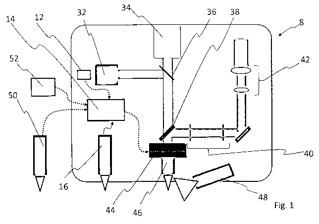
Fig. 1 shows an laser processing system 8 according to the invention, such as
that preferred
in the method according to the invention and the device 30 according to the
invention for
creating modifications 2 in a solid state 1.
The laser processing system 8 here has at least one laser bean source 32, in
particular with
focus marking. The laser beam source 32 may specifically be a coaxial light
source with
focus marking. The beams of light 10 generated by the laser beam source 32 are
preferably
directed on a predetermined path from the laser beam source 32 to a focus
device 44 or an
adjusting device 44 for adjusting the size of the focus and the position of
the focus in the
solid state 1. The adjusting device 44 here may preferably be a fine-focusing
device, in
particular for focusing in Z direction or in the direction of the laser beam.
The adjusting
device 44 may preferably be designed as a piezo fine-focusing device. The
laser beams 10
that pass through the adjusting device 44 preferably pass through a microscope
with a long
working distance 46. The laser beam is preferably adapted and/or adjusted
and/or modified
especially preferably by the microscope with the long working distance 46 and
the adjusting
device 44 in such a way that the modification 2 is created in the predefined
location. For
example, it is conceivable here for modification 2 to be created at a location
which deviates
less than 5 pm and preferably less than 2 pm and especially preferably less
than 1 pm from
the predefined location or is at a distance therefrom. The adjusting device 44
is preferably
controlled by a control system 14, wherein the control system 14 preferably
calculates and/or
determines and/or uses the position and orientation of the solid state 1 with
respect to the
laser processing system 8 or the distance of the current surface portion into
which the laser
beam is to be introduced, relative to the laser processing sytem 8 and the
local refractive
index or the average refractive index of the solid-state material and the
depth of processing
of the solid state 1 at the respective location for the adjustment of the
laser processing
system 8, in particular at least the adjusting device 44. The control system
14 can detect
26
CA 03010394 2018-06-29
Kehl, Ascherl, Liebhoff & Ettmayr 12 December
2016
Patent Attorneys ¨ Partnership Our Ref.:
5015-60-PCT
and/or receive the required data in real time through corresponding sensor
systems and/or
sensor means, which are thus connected to communicate. Alternatively however
it is also
conceivable for an analysis of the surface over which the laser beams 10
penetrate into the
solid state 1 to create the modifications 2 to be performed and/or carried out
for one or both
of the refractive index and processing depth parameters prior to the start of
processing.
These parameters can then be stored and/or entered into a memory device, i.e.,
a data
memory 12, in the form of corresponding location-dependent data. The data
memory 12 here
may be a variable medium, in particular a memory card or a permanently
installed memory
as part of the laser processing system 8.
Alternatively, however, it is also conceivable for the data memory 12 to be
set up outside of
the laser processing system 8 and to be connectable at least temporarily so
that it can
communicate with the laser processing system 8. Additionally or alternatively,
work
sequences or changes in the work sequence can be preselected for the control
system 14 by
a user 52. Furthermore, it is also conceivable for the data memory 12 to be
embodied as a
component of the control system 14. Additionally or alternatively, distance
data can be
detected by means of a sensor system 16 regarding the distance between the
predetermined
surface points on the solid state and the laser processing system 8. This
distance data is
preferably also supplied to the control system 14 for processing.
In addition, it is conceivable for the laser beam processing system 8 to have
a camera 34, in
particular a coaxial focus camera. The camera 34 is preferably arranged in the
direction of
the beam path of the laser beams 10 emitted by the laser processing system 8.
It is also
conceivable here for an optical element 36, in particular a partially
transparent mirror, to be
arranged in the optical field of the camera 34. The laser beams 10 are
preferably fed into the
optical field of the camera through the optical element 34.
In addition, it is conceivable that an additional optical element 38 and/or a
diffractive optical
element, in particular a beam splitter 38 is provided. A portion of the laser
beam 10 can be
deflected and/or separated from the main beam here by the beam splitter 38.
Furthermore
the separated and/or deflected portion of the laser beam can be modified by an
optional
spherical aberration compension 40 and/or by an optional beam widening 42.
27
CA 03010394 2018-06-29
Kehl, Ascherl, Liebhoff & Ettmayr 12 December
2016
Patent Attorneys ¨ Partnership Our Ref.:
5015-60-PCT
Furthermore, reference numeral 48 denotes a fluid-providing device 48 that is
preferably
provided, in particular for supplying a cooling fluid. A temperature control,
in particular
cooling, of the solid state 1 and/or of the microscope can preferably be
induced by means of
the fluid supply system 48.
Reference numeral 50 denotes a refractive index determination means which can
preferably
also analyze transparent and reflective surfaces. The refractive index is
preferably
determined by using the refractive index determination means 50 prior to
creation of the
modification. Alternatively, it is also conceivable here for the refractive
index to be
determined on another installation and for the data thereby detected to be
supplied to the
existing laser processing system 18 by data transfer.
The dotted lines illustrated in Fig. 1 with an arrow preferably characterize
data and/or signal
transmissions.
Fig. 2a shows schematically a preferred arrangement of the device components,
namely the
laser processing system 8, the receiving device 18 and the drive and/or
traversing device 22
of the device 30. It can be seen that the solid state 1 according to this
arrangement is
preferably situated between the receiving device 18 and the laser processing
system 8. The
solid state 1 is preferably glued to the receiving device 18, but it is also
conceivable for it to
be pressed thereto.
Fig. 2b shows an arrangement after creation of the modifications 2 and/or
after complete
creation of the crack guidance region 4. According to this illustration, a
receiving layer or
polymer layer 26 is arranged and/or formed on the surface 24 of the solid
state 1, through
which the laser beams 10 penetrate into the solid state 1. In addition a
functional fluid source
is characterized by the device 54 which outputs the functional fluid 56. The
functional fluid 56
is preferably liquid nitrogen. Thus the receiving layer 26 is cooled by the
functional fluid 56 to
a temperature below 20 C, in particular to a temperature below 10 C or to a
temperature
below 0 C or to a temperature below the glass transition temperature of the
polymer material
of the receiving layer 26. High mechanical stresses are created by the cooling
of the
receiving layer 26, causing a crack to propagate along the crack guidance
region 4.
28
CA 03010394 2018-06-29
Kehl, Ascherl, Liebhoff & Ettmayr 12 December
2016
Patent Attorneys ¨ Partnership Our Ref.:
5015-60-PCT
Fig. 3a shows, merely as an example, the relationship between a surface
profile of a solid
state 1 and the refractive index of the solid-state material. The values shown
on the
horizontal axis are in units of pm.
Fig. 3b shows examples of deviations of the material to be lasered (surface
profile and lateral
variations in the refractive index) as well as the laser focus position (no
AF: without
autofocus, the surface profile is written into the material in inverse ratio,
increased by the
refractive index, while a standard AF reverses this inversion so that the
surface profile is
transmitted with an n-fold gain; nAF: this takes into the account the
refractive index of the
substrate and/or the refractive index as a fixed factor so that the surface
profile is thereby
transmitted 1:1 into the material. AAF: knowledge of the average refractive
index of the
substrate and the target depth, the desired advanced autofocus function can
write a precisely
horizontal plane into the material).
Fig. 4a shows merely as an example various control positions of the laser
focus. The values
indicated on the horizontal axis are given in units of pm. Thus, the waveform
can be
determined as a control input variable for the position of the laser head in
various cases:
nAF (n-aware AF): the outer focus guide variable of the surface for correcting
the average
refractive index (n) of the surface. Thus the surface deviation can be
transmitted 1:1 into the
volume. Therefore, theoretically, the wafer to be split off will not have any
fluctuations in
thickness (TTV). However, the topography and thus the poor planarity are
maintained both
for the wafer and for the remaining ingot.
AAF (advanced AF): to correct the autofocus guide variable of the surface with
knowledge of
the average refractive index of the surface and the correction plane of the
surface. It is thus
possible to prepare a flat laser plane that prepares the semiconductor crystal
to be very flat
for additional splits with an inexpensive polishing step. However, the wafer
that is split off is
flat on one side immediately after the split but has a greater thickness
deviation.
AnAF (Advanced n-aware AF): to correct the autofocus guide variable of the
surface with
knowledge of the local refractive index of the surface and the correction
plane of the surface.
Thus, a flat laser plane, which prepares the semiconductor crystal to be very
flat for
29
CA 03010394 2018-06-29
Kehl, Ascher!, Liebhoff & Ettmayr 12
December 2016
Patent Attorneys ¨ Partnership Our Ref.:
5015-60-PCT
additional splits with an inexpensive polishing step, is possible even with
heterogeneous
samples with prior knowledge.
The present invention thus relates to a method for creating modifications in a
solid state,
wherein a crack guidance region for guiding a crack for separation of a solid-
state
component, in particular a solid-state layer from the solid state is
predefined by the
modification. The method according to the invention here preferably comprises
at least the
following steps:
Moving the solid state relative to a laser processing system, creating in
succession a plurality
of laser beams by means of the laser processing system for creating at least
one
modification, wherein the laser processing system is adjusted for defined
focusing of the
laser beams continuously as a function of a plurality of parameters, in
particular at least two
= parameters. A planar microfocus for multiphoton material processing in
the volume is
preferably made possible by the method according to the invention.
Fig. 5a shows a Raman instrument 58. The Raman instrument 58 shown here has a
laser 60
for emitting laser rays. The laser rays are preferably sent by means of at
least one optical
fiber 61 for excitation preferably through a lens and preferably focused by
this lens 64 in
particular being focused in the solid state. This radiation is at least
partially scattered,
= wherein light components having the same wavelength as the radiation
emitted by the laser
are preferably filtered out by means of a filter device and/or an exciting
filter 62. The other
radiation components are then sent to a spectrograph 68 and detected by means
of a
camera system, in particular a CCD detector 70 and processed and/or analyzed
by a control
system 14, 72, in particular a computer.
Thus atomic vibrations in the crystal are excited preferably by an external
laser or especially
preferably by an additional laser. The vibrations are generated by light
scattering on crystal
atoms, which leads to observable scattered light, which has a photon energy
that is altered
by the amount of the vibration energy. When there are multiple excitable
vibrations, multiple
peaks also appear in the spectrum of the scattered light. Then using a
spectrometer (grating
spectrometer), the resulting Raman scattering spectrum can be investigated in
greater detail
(so-called Raman spectroscopy). In this method, the local conditions in the
crystal are
CA 03010394 2018-06-29
Kehl, Ascherl, Liebhoff & Effmayr 12 December
2016
Patent Attorneys ¨ Partnership Our Ref.:
5015-60-PCT
imposed on the individual Raman lines in their shape, and it is possible to
deduce the degree
of doping by analyzing the shape of the Raman line.
Fig. 5b shows how possible lattice vibrations appear in SIC, wherein these
modes are
predetermined by crystal symmetry and directions and may also be excited at
the same time.
The views shown here have one direction along the crystal axis A. Atomic
vibrations here are
possible only in certain directions, the directions being predetermined by the
symmetry of the
crystal.
Fig. 6a shows a detail of a Raman diagram of a 4H-silicon carbide solid state
doped with
nitrogen (example of a Raman spectrum on doped SiC). The shape of the LO(PC)
mode is
used here for measuring the dopant concentration and is fitted. Bottom panel:
fitting residual.
Fig. 6b shows a smaller detail of the Raman spectrum.
As shown here, this yields a direct method for determining the dopant
concentration with
Raman measurements from a measurement of teh shape and subsequent fitting to
the
LO(PC) mode.
In general, the goal is thus, by adjusting the laser parameters, to adjust the
optimum (least
possible, shortest possible) path of cracking in the material which will still
lead to successful
separation due to crack propagation but will otherwise minimize or reduce all
loss of material
(including that in grinding operations).
Fig. 7a and Fig. 7b show two possibilities for lifting a single wafer from the
boule/ingot.
According to Fig. 7a this is embodied as a feed-foward loop and according to
Fig. 7b it is
embodied as a feedback loop.
In feed-forward, the distribution before the laser process is characterized
and then used to
calculate a map and/or treatment instructions and/or parameter adjustments, in
particular as
a function of location, for laser process, in particular for creation of the
modification. Feed-
forward is preferably carried out on the ingot/boule.
31
CA 03010394 2018-06-29
Kehl, Ascher!, Liebhoff & Ettmayr 12 December
2016
Patent Attorneys ¨ Partnership Our Ref.:
5015-60-PCT
Alternatively, as illustrated in Fig. 7b, a feedback loop may be implemented,
so that the
resulting wafer is characterized after each separation step and then serves as
a template for
the next.
Depending on the material and the doping, different adjustments can thus be
made during
the laser process.
With the SIC material, different adjustments in the laser parameters can be
made at different
depths as a function of the doping. This can lead to the functions also shown
below with the
boundary conditions listed below:
Depth 180pm, pulse duration 3 ns, numerical aperture 0.4
Low doping: 7 pJ-21 mOhmcm
High doping: 8 pJ-16 mOhmcm
Depth 350pm, pulse duration 3 ns, numerical aperture 0.4
Low doping: 9.5 pJ-21 mOhmcm
High doping: 12 pJ-16 mOhmcm
Formula for a depth of 180 pm:
= energy in pJ
EO offset energy at the lowest doping
= energy scaling factor
= measured degree of doping
= basic degree of doping (21 mOhmcm)
E = E0+(B-R)*K
where
K = 1/(21-16) pJ/mOhmcm = 0.2 pJ/mOhmcm
EC) = 7pJ
B = 21 mOhmcm
Example: measured degree of doping of 19 mOhmcm: E = 7.4 pJ
32
CA 03010394 2018-06-29
Kehl, Ascher!, Liebhoff & Ettmayr 12 December
2016
Patent Attorneys ¨ Partnership Our Ref.:
5015-60-PCT
Formula for 350 pm depth:
E energy in pJ
E0 offset energy at the lowest doping
K energy scaling factor
R measured degree of doping
B basic degree of doping (21 mOhmcm)
E = E0+(B-R)*K
where
K = 2.5/(21-16) pJ/mOhmcm = 0.5 pJ/mOhmcm
EC) = 9.5 pJ
B = 21 mOhmcm
Example: measured degree of doping of 19 mOhmcm: E = 10.5 pJ
33
CA 03010394 2018-06-29
Kehl, Ascherl, Liebhoff & Ettmayr 12 December
2016
Patent Attorneys ¨ Partnership Our Ref.:
5015-60-PCT
List of Reference Numerals
1 solid state 50 refractive index determination
2 modification means
4 crack guidance region 52 user
6 solid-state portion 54 functional fluid source
8 laser processing system 56 functional fluid
laser beam 58 Raman instrument
12 data memory device 60 laser
14 control system 61 optical fiber for excitation
16 sensor device 62 excitation filter
18 receiving device 64 lens
axis of rotation 68 spectrograph
22 drive device 70 CCD detector
24 surface of the solid-state portion to 72 analysis and/or
processing system
be separated or control system 14
26 receiving layer 74 inspection
device 76 adjusting of laser parameters
32 laser beam source and/or machine parameters and
34 camera generating spatially resolved
36 optical element treatment instructions and/or a
38 beam splitter spatially resolved treatment map
spherical aberration compensation 78 laser process (generating
means modifications)
42 beam expander 80 separation step, in particular by
44 adjusting device means of crack propagation and
46 microscope with a long working crack guidance
distance 82 surface treatment
48 fluid source
34