Note : Les descriptions sont présentées dans la langue officielle dans laquelle elles ont été soumises.
CA 03013205 2018-07-30
WO 2017/132280
PCT/US2017/014977
1
MULTI-LAYER PHOTO DEFINABLE GLASS WITH INTEGRATED DEVICES
Technical Field of the Invention
Photo-definable glass-ceramic has a mechanical distortion during processing as
a function of
temperature and time. The present invention relates to creating multi-layer
and single layer
photo-definable structures, that can contain electronic, photonic, or MEMS
devices to create
.. unique vertically integrated devices or system level structures that
virtually eliminate mechanical
distortions that result from metallization.
Background Art
Photosensitive glass structures are being used for a number of micromachiming
and
microfabrication processes such as integrated electronic photonics and MEMs
devices in
.. conjunction with other elements systems or subsystems on a planer
structure. Over the last
number of years, to achieve higher performance and packing densities, the
packaging industry has
been integrating multiple layers of silicon devices connected through metal
filled via, epoxies and
other elements in conjunction with thermal and/or UV curing processes. To
date, all photo-
definable glasses have feature migration as a function temperature cycling
that, if not controlled,
randomly moves the previously created device structures in the glass.
Photo-definable glass ceramic (APEX ) or other photo definable glass as a
novel substrate
material for semiconductors, RF electronics, microwave electronics, electronic
components
and/or optical elements. In general, a photo definable glass is processed
using first generation
semiconductor equipment in a simple three step process and the final material
can be fashioned
into either glass, ceramic, or contain regions of both glass and ceramic. A
photo definable glass
ceramic possesses several benefits over current materials, including: easily
fabricated high
density vias, demonstrated microfluidic device capability, micro-lens or micro-
lens array,
transformers, inductors transmission lines, and many other devices. Photo-
sensitive glasses have
several advantages for the fabrication of a wide variety of microsystems
components.
Microstructures have been produced relatively inexpensively with these glasses
using
conventional semiconductor or PC board processing equipment. In general,
glasses have high
temperature stability, good mechanical and electrical properties, and have
better chemical
resistance than plastics and many metals. Another form of photo-sensitive
glass is
FOTURANt, made by Schott Corporation. FOTURAN comprises a lithium-aluminum-
silicate
glass containing traces of silver ions plus other trace elements specifically
silicon oxide (SiO2) of
75-85% by weight, lithium oxide (Li2O) of 7-11% by weight, aluminum oxide
(A1203) of 3-6%
by weight, sodium oxide (Na2O) of 1-2% by weight, 0.2-0.5% by weight
antimonium trioxide
(Sb203) or arsenic oxide (As203), silver oxide (Ag2O) of 0.05-0.15% by weight,
and cerium
2
oxide (Ce02) of 0.01-0.04% by weight. As a photo-definable glass is cycled to
high temperature,
glass transformation temperature (e.g., greater than 465 C. in air for FOTURAN
) it experiences a
color shift from transparent to yellow. This measureable color shift is
directly related to the time
and temperature. The higher the temperature and the longer the time the
greater the color shift. The
color shift makes it an easy method to determine the thermal cycle history of
a fully processed
photo-definable glass.
When exposed to UV-light within the absorption band of cerium oxide the cerium
oxide acts as
sensitizers, absorbing a photon and losing an electron that reduces
neighboring silver oxide to form
silver atoms, e.g.,
Ce3+ + Ag+ = Ce' + Ag
The silver atoms coalesce into silver nanoclusters during the baking process
and induce nucleation
sites for crystallization of the surrounding glass. If exposed to UV light
through a mask, only the
exposed regions of the glass will crystallize during subsequent heat
treatment.
This heat treatment must be performed at a temperature near the glass
transformation temperature
(e.g., greater than 465 C. in air for FOTURAN ). The crystalline phase is more
soluble in etchants,
such as hydrofluoric acid (HF), than the unexposed vitreous, amorphous
regions. In particular, the
crystalline regions of FOTURAN are etched about 20 times faster than the
amorphous regions in
10% HF, enabling microstructures with wall slopes ratios of about 20:1 when
the exposed regions
are removed. See T. R. Dietrich et al., "Fabrication technologies for
microsystems utilizing photo-
sensitive glass," Microelectronic Engineering 30, 497 (1996).
The act of converting the photo definable glass to near the glass
transformation temperature (e.g.,
greater than 465 C. in air for FOTURAN ) facilitate etching and formation of
complex three
dimensional structures for inducing a permanent mechanical distortion in the
substrate. These
random distortions can be as large as 400 um. Distortions greater than tens of
microns prevent the
alignment of integral electronic elements including: vias, bonding pads,
interconnect, fiber
alignments, sensors and other integrated devices making the device virtually
impossible to
successfully integrate with other packaging elements. The distortion, created
by processing photo
definable glass to near the glass transformation temperature, can be
successfully controlled with
composition as demonstrated by APEX Glass. Even the compositional changes
from APEX
Glass are unable to prevent the mechanical distortion associated with copper
paste metallization.
.. Various forms of metal pastes can be used for metallization of glass,
ceramic or other substrates.
These metal pastes include: silver, gold, and copper. Although all of these
metal pastes will
CA 3013205 2020-02-07
CA 03013205 2018-07-30
WO 2017/132280
PCT/US2017/014977
3
work for the application, copper paste metallization has become the industry
standard due to both
cost and performance, plus historical packaging and processing technology.
Unfortunately,
copper paste metallization has a temperature processing range and time profile
up to 600 C for up
to an hour. These times and temperatures induce a random shift in the physical
dimensions of
each glass substrate making it impossible to align structures or create
structures between other
to glass layers, bonding pads or other packaging elements. As a result, the
ability to package a glass
substrate with copper paste metallization is impossible. However, multiple
thermal cycles
exacerbate the random theimal creep and induces an optical change to the
transmission of all
photo-definable glass even the compositionally stabilized photo-definable
glass. This invention
provides for a cost effective method to produce copper paste metalized photo-
definable glass
either as a single layer or multiple layer of photo-definable glass structure
minimizing and/or
eliminating the thermal creep, thus enabling reliable single/multi-level
vertical interconnects and
monolithic device and copper paste metallization. The mechanical distortion
can enable multi-
level device structures having one or more parts of the device contained on
separate photo-
definable glass layers.
Disclosure of the Invention
The present invention includes a method to fabricate a multi-layer and single
layer photo-
definable structures, that can contain electronic, photonic, or MEMS with
copper metallization.
The multi-layer structure enables the interface of two or more photo-definable
glass wafers with
reliable multi-level vertical interconnects and monolithic device where part
of the device is
contained on each glass layer.
A method of fabrication of single or multi-layer photo-definable glass
structure with a
plurality of devices on each layer with copper paste metallization comprising
of one or more,
electronic, photonic, or MEMS device. The metallization process uses a metal
paste that requires
a thermal ramp rate of 10 C/min from 25 C to 600 C, a 10 min hold at 600 C and
ramp down
from 600 C to 25 C. This approximate 35-minute annealing cycle is all
accomplished in
nitrogen to prevent oxidation of the copper. In general, the metallization
thermal cycle induces a
permanent random physical distortion and optical transmission change in the
photo-definable
glass structure. A process flow is required to minimize the time and
temperature for the
annealing cycle to melt and densify the copper paste into solid metallic
structure while not
exposing the glass to long duration time and temperature cycles.
The photo-definable glass is transparent to several parts of the
electromagnetic spectrum. Several
portions of the photo-definable glass' transparent electromagnetic spectrum
are absorbed by
copper and copper paste. The electromagnetic spectrum that is absorbed by
metals and nominally
4
.. transparent to a photo-definable glass enables the melting and
densification of the copper paste
metallization of a traditional glass or photo definable glass substrate. The
electromagnetic
spectrum that can achieve melting and densification of copper paste on a glass
substrate
includes but not limited to microwave frequency, visible, near infra-red and
mid infra-red
spectrum that can be generated by an inductive, microwave, or high intensity
lamp.
In accordance with an aspect of at least one embodiment, there is provided a
method for
producing a fully dense metallized photo-definable glass structure where a
metal is
preferentially heated and densified relative to the photo-definable glass
structure comprising:
providing a single-layer photo-definable glass substrate or a multi-layer
photo-definable glass
substrate that contains a plurality of electronic, photonic, or micro
electrical mechanical system
devices; depositing a copper paste on the single-layer photo-definable glass
substrate or the
multi-layer photo-definable glass substrate; and annealing the copper paste to
densify it by
heating it under nitrogen to prevent oxidation of the copper paste with a
thermal ramp rate of
10 C/min from 25 C to 600 C, a 10 mm hold at 600 C; and ramp down from 600 C
to 25 C;
wherein a change in a position of the copper paste, of the single-layer photo-
definable glass
.. substrate, or of the multi-layer photo-definable glass substrate after the
annealing step is less
than 201.1m; and wherein a change in a wavelength of a color of the single-
layer photo-definable
glass structure or of the multi-layer photo-definable glass structure is less
than or equal to
75nm.
In accordance with an aspect of at least one embodiment, there is provided a
method of
.. integrating two or more photo-definable glass structures where one or more
metal structures
are preferentially heated and densified relative to the two or more photo-
definable glass
structures, comprising: providing two or more photo-definable glass substrates
that contain a
plurality of electronic, photonic, or micro electro mechanical system devices;
depositing a
copper paste on the two or more photo-definable glass substrates; and
annealing the copper
paste to densify it by heating it under nitrogen to prevent oxidation of the
copper paste with a
thermal ramp rate of 10 C/min from 25 C to 600 C, a 10 mm hold at 600 C; and
ramp down
from 600 C to 25 C; wherein a change in a position of the copper paste or the
two or more
photo-definable glass substrates after the annealing step is less than 201.1m;
and wherein a
change in a wavelength of a color of the two or more photo-definable glass
substrates is less
.. than or equal to 75nm.
Date Recue/Date Received 2020-07-02
4a
In accordance with an aspect of at least one embodiment, there is provided a
method for
producing a single-layer photo-definable glass substrate or a multi-layer
photo-definable glass
substrate with one or more devices on a layer of the single-layer photo-
definable glass structure
or on each of the layers of the multi-layer photo-definable glass structure
comprising: providing
a single-layer photo-definable glass substrate or a multi-layer photo-
definable glass substrate
with one or more electronic, photonic, or micro electro mechanical system
devices on the layer
of the single-layer photo-definable glass substrate or on each of the layers
of the multi-layer
photo-definable glass substrate; depositing a copper paste on the single-layer
photo-definable
glass substrate or the multi-layer photo-definable glass substrate; and
annealing the copper
paste to densify it by heating it under nitrogen to prevent oxidation of the
copper paste with a
thermal ramp rate of 10 C/min from 25 C to 600 C, a 10 min hold at 600 C; and
ramp down
from 600 C to 25 C.
Description of the Drawings
For a more complete understanding of the features and advantages of the
present invention,
reference is now made to the detailed description of the invention along with
the accompanying
figures and in which:
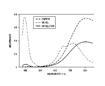
FIGURE 1 shows a graph of the absorption spectra for copper.
FIGURES 2A and 2B show a graph of the absorption spectra for APEX glass.
FIGURE 3 shows a graph of the optical spectra for APEX glass after different
thermal
cycling and UV exposure.
FIGURE 4 shows a graph of the temperature cycle for a silicon substrate for a
rapid
thermal annealing source.
FIGURE 5 shows a graph of the optical spectra for a rapid thermal annealing
source.
Description of Embodiments
While the making and using of various embodiments of the present invention are
discussed in
detail below, it should be appreciated that the present invention provides
many applicable
inventive concepts that can be embodied in a wide variety of specific
contexts. The specific
embodiments discussed herein are merely illustrative of specific ways to make
and use the
invention and do not restrict the scope of the invention.
Date Recue/Date Received 2020-12-21
4b
.. FIGURE 1 shows a graph of the absorption spectra for copper. FIGURES 2A and
2B show a
graph of the absorption spectra for APEX glass. FIGURE 3 shows a graph of the
optical
spectra for APEX glass after different thermal cycling and UV exposure.
FIGURE 4 shows a
graph of the temperature cycle for a silicon substrate for a rapid thermal
annealing source.
FIGURE 5 shows a graph of the optical spectra for a rapid thermal annealing
source.
A source of the electromagnetic spectrum that is absorbed by metals and is
nominally
transparent to a photo-definable glass enables the heating, melting and
densification of the
metal deposited from a paste deposition process on a traditional glass or
photo definable glass
substrate is preferably a high intensity tungsten filament lamp. High
intensity tungsten filament
lamps are the heating source used in rapid thermal annealing (RTA) or rapid
thermal processing
(RTP). The time at temperature is such that it does not change the position of
the features on
the substrate by
CA 3013205 2020-02-07
CA 03013205 2018-07-30
WO 2017/132280
PCT/US2017/014977
5 greater 20p,m and the color shift of the glass is less than 75nm.
Experiments have shown that the
time needs to be less than 10min at 700 C or a temperature time ratio of less
than 70 C/min.
RTA is a process used in semiconductor device fabrication that consists of
preferentially heating
a single metal on a glass substrate or a stack of glass substrates.
Traditional RTA process can be performed by using either lamp based heating, a
hot chuck, or a
hot plate that a substrate. A hot chuck or a hot plate RTA will heat the
substrate in addition to
glass substrate. Lamp based heating RTA processes will heat the metal
significantly more than
the surrounding glass substrate allowing the metal to be heat-densified
without inducing the
permanent mechanical distortion or optical change in the glass substrate.
The electromagnetic spectrum that can achieve melting and densification of
copper paste on a
glass substrate includes but not limited to microwave frequency, visible, near
infra-red and mid
infra-red spectrum that can be generated by an inductive, microwave, or high
intensity lamp.
To facilitate the understanding of this invention, a number of terms are
defined below.
Terms defined herein have meanings as commonly understood by a person of
ordinary skill in
the areas relevant to the present invention. Terms such as "a", "an" and "the"
are not intended
to refer to only a singular entity, but include the general class of which a
specific example may
be used for illustration. The terminology herein is used to describe specific
embodiments of the
invention, but their usage does not delimit the invention, except as outlined
in the claims.
Although the present invention and its advantages have been described in
detail, it should be
understood that various changes, substitutions and alterations can be made
herein without
departing from the spirit and scope of the invention as defined by the
appended claims. Moreover,
the scope of the present application is not intended to be limited to the
particular embodiments of
the process, machine, manufacture, composition of matter, means, methods and
steps described in
the specification. As one of ordinary skill in the art will readily appreciate
from the disclosure of
the present invention, processes, machines, manufacture, compositions of
matter, means,
methods, or steps, presently existing or later to be developed, that perform
substantially the same
function or achieve substantially the same result as the corresponding
embodiments described
herein may be utilized according to the present invention. Accordingly, the
appended claims are
intended to include within their scope such processes, machines, manufacture,
compositions of
matter, means, methods, or steps.