Note : Les descriptions sont présentées dans la langue officielle dans laquelle elles ont été soumises.
1
METHODS FOR MICRO AND NANO FABRICATION BY
SELECTIVE TEMPLATE REMOVAL
FIELD
The present invention relates generally to methods of fabrication of
micro and nano-structures. More particularly, the present invention relates to
methods of fabrication of micro and nano-structures using selective removal of
a
thin-film material deposited on a micro or nano-structure template.
BACKGROUND
In conventional micro- and nano-fabrication, there are variety of
cases in which a specific patterned thin-film material may need to be made.
Examples may include production of micro- or nano-structure patterned thin-
film
electrical contacts on an electronic chip; micro- or nano-structure patterned
perforated metallic film(s) in a plasmonic device; micro- or nano-structure
textured electrodes for photo-voltaic cells, plasmonic devices, metamaterial
devices, optical filters, bio-sensors, gas detectors, optical polarizers,
displays,
document security features, among many others.
In conventional micro- and nano-fabrication, there are also a variety
of cases in which a specific spatial arrangement of precisely shaped micro- or
nano-particles may need to be made. Examples may include production of
micro- or nano-particles and structures as may be used in such applications as
those listed above.
There are conventionally known methods that rely on established
micro- or nano-fabrication processes that may provide for fabrication of micro-
or
nano-structures as may be used in such applications as those listed
previously.
Typically such conventional processes are often utilized for manufacturing
many
individual and separate small devices on a shared large wafer (e.g. silicon
1
CA 3014989 2018-08-22
2
wafer). The total fabrication cost of producing a micro- or nano-structured
wafer
will be divided among the many separate individual devices that are
manufactured on the same wafer; and therefore the cost of conventional
manufacture of each device is typically defined by the cost per area of the
wafer
containing multiples of those conventional small devices.
However, there are cases in which the final micro- or nano-
structure based device need to be large (such as for example >1cm2) in area.
Using conventional known wafer-scale micro- or nano-fabrication methods will
typically make such large area devices undesirably or unfeasibly expensive for
many potential applications. For example, a plasmonic color filter may
comprise
a 30nm metal film perforated with 100nm diameter holes periodically arranged
in
a lattice of 200nm pitch or periodicity. As an example, the desired size of a
plasmonic-based color filter should be in the range of ¨25cm2 area for
lighting or
photography applications, the filtering efficiency should be high, and a
desired
price for such applications should be low (perhaps $1 per filter or less). If
the
filter is to be disposable, a high volume (millions or billions) of such
devices
should be reasonably produced. Such a relatively large area and relatively
inexpensive price per device may not be possible using conventionally known
fabrication processes where the cost of such a nano-structured filter device
may
typically be one or more orders of magnitude higher than desired for such an
application.
In one conventional method, optical lithography may be used to
make micro- or nano-structures in a thin-film material. The process typically
involves: (i) optical resist coating, exposure, and development steps, (ii)
thin-film
material coating steps, and (iii) steps (e.g. wet etching, dry etching, and
lift-off) to
transfer patterns of the resist to the thin-film. In optical lithography many
wafers
can be patterned using a single often expensive optical mask; therefore the
cost
of the mask is divided among the many final patterned wafers, though the cost
per unit area of the final wafer may still remain significantly higher than
that which
is desired due to the many steps that are required to pattern a final device.
Also,
the optical lithography often covers a range of minimum feature sizes larger
than
2
CA 3014989 2018-08-22
3
what may typically be needed for such applications as those listed above. Of
special interest is the fabrication of precision nano-structures for which
optical
lithography typically may provide poor results. There are a range of
conventional
direct (i.e. maskless) fabrication methods that maybe used to directly pattern
the
final wafer at micro- or nano-sizes.
In one conventional maskless method, a focused ion beam (FIB)
may be used to make micro- or nano-structures from a thin-film material
deposited on a plain substrate. FIB may be used to mill features even smaller
than 15nm in a thin-film. However, such a method has the disadvantage of being
very low throughput, which typically limits the practical device area to
undesirably
small sizes (e.g. < 1cm2).
In another conventional maskless method, Electron Beam
Lithography (EBL) may be used to fabricate micro- or nano-structures. The
process typically involves: (i) coating a substrate with a thin-film material,
(ii)
electron beam lithography to make openings in a resist that is spun on the
thin-
film, and (iii) reactive ion etching to etch through the thin-film that is not
protected
with the resist. Another typical process involves: (i) electron beam
lithography to
make openings in a resist that is spun on the substrate, (ii) coating the
resist and
the openings with a thin-film material, and (iii) lifting-off the material
that is
deposited on the resist by dissolving the resist in appropriate chemicals. EBL
has
a higher throughput compared to FIB; and that makes fabrication of larger area
devices possible. However, EBL has the disadvantage of being too slow and too
expensive for directly fabricating many large area micro and nano-structured
devices.
In another conventional maskless method, interference lithography
may be used to fabricate micro- or nano-structures. The process typically
involves: (i) coating a substrate with photoresist, (ii) one-step or few-step
interference lithography followed by resist development to yield periodic
resist
structures on the substrate, (iii) thin-film material deposition, and (iv)
lift-off the
thin-film from photoresist. Interference lithography is faster than EBL, and
it can
yield fast patterning of larger areas. However, interference lithography is
3
CA 3014989 2018-08-22
4
considerably restricted in the shape and precision of the final patterns
possible to
make, and the materials which are compatible for this process.
In another conventional method, polystyrene nanospheres are self-
assembled on a substrate. Subsequent reactive ion etching may be used to
shrink the size of spheres to desired value. Thin-film material deposition on
the
spheres and lift-off yields periodic micro- or nano-structures. However, such
nanosphere lithography is typically limited in control over the type of
fabricated
structures and their uniformity.
Such typical conventional processes rely on well-established micro-
or nano-fabrication techniques to yield a single device or plurality of
devices that
share a single host wafer. That means to make another copy of the same
device, almost the entire process must be undesirably repeated, which
typically
is a significant limitation for industrial scale production of desirably
inexpensive
large devices. However, the above conventional techniques or others in the art
may be used to yield a single expensive master wafer with a template of
patterns
that may be replicated to many cheap copies using one of the known
conventional replication methods.
In one conventional replication method, nanoimprint lithography
may be used to replicate the micro- or nano-structures of an expensive master
which is made by one of the conventional techniques listed above or others
known in the art. The process typically involves: (i) bringing a polymer/resin
in
contact with the master surface and curing it in place, (ii) peeling off the
hardened polymer/resin from the master. The peeled polymer/resin will carry a
replica of the patterns on its surface. The process can be repeated many times
to get many cheap replicas from a single master.
In another conventional replication method, soft lithography may be
used to replicate the micro- or nano-structures of an expensive master. The
process typically involves: (i) making a soft replica of a master wafer by
nanoimprint lithography, (ii) coating the target substrate with a photoresist,
(iii)
bringing the soft replica in conformal contact with the target wafer, and (iv)
UV
exposure. Developing the exposed resist will result in a replica of the master
to
4
CA 3014989 2018-08-22
5
the target substrate.
In another conventional replication method, roll-to-roll nanoimprint
lithography (also known as 'cast and cure', 'roll-to-roll UV casting', and
'roll-to-roll
embossing') may be used to replicate the micro- or nano- structures of an
expensive master. The process typically involves: (i) replicating a master
into a
flexible copy using nanoimprint lithography, soft lithography, etc. and/or
further
processing the copy to a metal (e.g. Ni) shim, and (ii) rolling the flexible
copy
over a mold roller which is pressed against a back roller. Similar to a
printing
machine, a thin substrate moves between the two rollers where it receives a
copy
of the patterns through a thermal or UV process. The massive throughput of a
roll to roll process can cheaply replicate micro- and nano-patterns over a
giant
surface at a high speed. A variation of the same process can be implemented in
a plate-to-roll format.
Such conventional replication techniques and others in the art
typically provide a resin/plastic copy of a typically expensive master. One
still
needs to employ metal/material deposition, lift-off, etching, etc. to yield a
final
device that includes a micro or nano-structured thin-film material. Any
process
that can yield a micro or nano-structured thin-film material that is more cost
effective than those known in the art, and without the use of lift-off or
etching is of
high industrial value, because it can reduce the cost and complexity of the
manufacturing process.
In one conventional method to avoid lift-off or etching, template
stripping may be used to selectively remove parts of a thin-film material
otherwise uniformly deposited over template (a master or a replica of a
master).
The process typically involves: (i) coating the template with a thin-film
material,
(ii) pressing the coated template against a plastic substrate while heating
the
sandwiched materials to a temperature above a glass transition temperature of
the plastic, and (iii) peeling of the cooled plastic. The process results in
the
transfer of a micro or nano structured thin-film material to plastic, leaving
behind
the thin-film in valleys of the template. The method leverages the poor
adhesion
of the thin-film to the template, and the good adhesion of the thin-film to
the
CA 3014989 2018-08-22
6
softened plastic.
Conventional template stripping may be implemented in different
variants. In one variant a UV curable resin is applied over the thin-film
coated
template to strip the deposited thin-film. In another variant, an adhesive is
applied over the thin-film coated template to strip the deposited thin-film.
In
another variant, the template is cleaned and reused at the start of each thin-
film
deposition and stripping cycle. In another variant, the ultra-smooth surface
formed at thin-film and template interface is brought to the top functional
surface
of the final perforated thin-film enhancing the final device performance. In
another variant, nano-tips for applications in near-field optical microscopy,
nano-
focusing, or others are fabricated using template striping. In another
variant, all
the thin-film material deposited over the template is transferred to a target
substrate to yield a very smooth textured surface.
All the variants of template stripping, whether used for stripping the
entire thin-film deposited on the template to make a very smooth surface, or
used
for stripping selected metal surface to make a micro- or nano-structured
material,
typically rely on specifically "poor" adhesion of the deposited thin-film
material to
the underlying template and a "strong" adhesion of the thin-film to an applied
resin/adhesive layer for removal. It avoids lift-off or etching, and yields a
low cost
and more environmentally friendly process. However, such striping techniques
typically rely on the use of adhesives to keep the final product on the final
substrate, and the template typically needs to be cleaned and prepared before
each use. Accordingly, such stripping techniques typically undesirably limit
the
structural robustness of the final product, the maximum throughput of an
industrial implementation of the process, the selection of template material
and/or
its anti-adhesion surface treatment, and the type of deposited thin-film
material.
Accordingly, there is a need for additional and improved methods of
fabrication of micro- or nano-structured thin-films on substrate surfaces
which
may desirably allow for reducing the manufacturing expense per unit area of
the
desired micro- or nano-structures. Furthermore, there is a need for additional
and
improved methods of fabrication of micro- or nano-structured thin-films on
6
CA 3014989 2018-08-22
substrate surfaces which may desirably increase the fabrication throughput.
There is also a need for additional and improved methods of fabrication of
micro-
or nano-structured thin-films on substrate surfaces which may desirably
increase
the product robustness and the range of possible used materials.
SUMMARY
Embodiments of the present invention relate to methods for
fabricating micro- and/or nano-structure from a thin-film material deposited
and
adhered to a template defining the micro- or nano-structures, while avoiding
lift-
off or etching.
According to one embodiment of the present invention, a method of
fabricating (i) a perforated thin-film comprising micro- or nano-structure
perforations on a substrate surface, and (ii) shaped and positioned micro- or
nano-particles encapsulated in a substrate is provided. The method of
fabrication comprises the steps of:
a) providing a micro- or nano-structure template comprising a
substrate surface and raised micro- and/or nano-structures extending
above the substrate surface;
b) depositing a single or a few thin-film coating(s) of a first
stack of suitable coating material(s) over the substrate and raised micro-
or nano-structures such that the thin-film coating(s) is substantially
adhered to layer over which they are deposited on, forms a thin-film cap,
such as an overhanging thin-film cap, on the raised micro- or nano-
structures, and the total thin-film thickness is less than the height of the
micro- or nano-structures above the substrate surface;
c) depositing a layer of a potting material (e.g. a UV curable
resin) over the first stack of thin-film coating(s) on the substrate and
raised
micro- or nano-structures such that the potting material is substantially
weakly adhered to the last deposited thin-film;
{00062201} 7
CA 3014989 2019-06-28
õ
d) hardening or curing the potting material such that the
hardened potting material encapsulates the thin-film caps on the raised
micro- or nano-structures; and
e) removing the hardened potting material from the first stack of
thin-film coated template such that the thin-film caps remain encapsulated
in the hardened potting material, to reveal: (i) a perforated thin-film coated
substrate, wherein the thin-film is perforated at the locations of the micro-
or nano-structures of the template, and (ii) micro- or nano-particles
encapsulated in the hardened potting material, wherein the particles are at
the locations of the micro- or nano-structures of the template and take
their shapes.
According to an alternative embodiment of the present invention,
step e) of the above-described method may optionally further comprise:
e) removing the hardened potting material from the first stack
of
thin-film coated substrate such that the thin-film caps and raised micro or
nano-structures are removed with the hardened potting material, to reveal:
(i) a perforated thin-film coated substrate, wherein the thin-film is
perforated at the locations of the micro or nano-structures of the template,
and (ii) micro- or nano-particles encapsulated in the hardened potting
material, wherein the particles are at the locations of the micro- or nano-
structures of the template and take their shapes.
According to another embodiment of the present invention, the method of
fabricating a perforated thin-film comprising micro- or nano-structure
perforations
on a substrate surface additionally comprises:
f) depositing a single or a few thin-film coating(s) of a second
stack of suitable coating material(s) over the substrate and raised micro-
or nano-structures such that the second thin-film coating(s) is substantially
adhered to the layer over which they are deposited on and forms a second
thin-film cap on the raised micro- or nano-structures;
g) depositing a layer of a potting material over the second stack
of thin-film coating(s) on the substrate and raised micro- or nano-
100062201 8
CA 3014989 2019-06-28
structures such that the potting material is substantially weakly adhered to
the last deposited thin-film;
h) hardening or curing the potting material such that the
hardened potting material encapsulates the second thin-film caps on the
raised micro- or nano-structures; and
i) removing the hardened potting material from the second
stack thin-film coated substrate such that the second thin-film caps remain
encapsulated in the hardened potting material, to reveal: (i) a perforated
first and second stack thin-film coated substrate, wherein the thin-film
stacks are perforated at the locations of the micro- or nano-structures of
the template, and (ii) micro- or nano-particles from the second thin-film
stack encapsulated in the hardened potting material, wherein the particles
are at the locations of the micro- or nano-structures of the template and
take their shapes.
According to a further embodiment of the present invention, another
method of fabricating (i) a perforated thin-film comprising micro- or nano-
structure perforations on a substrate surface, and (ii) shaped and positioned
micro- or nano-particles encapsulated in a substrate is provided. The method
of
fabrication comprises the steps of:
a) providing a micro- or nano-structure template comprising a
substrate surface and raised micro- or nano-structures extending above
the substrate surface;
b) depositing a single or a few thin-film coating(s) of a first
stack of suitable coating material(s) over the substrate and raised micro-
or nano-structures such that the thin-film coatings are substantially
adhered to the material over which they are deposited, and the overall
thin-film thickness is less than the height of the micro- or nano-structures
above the substrate surface;
c) depositing a layer of a potting material over the thin-film
coating on the substrate and raised micro- or nano-structures such that
1000622011 9
CA 3014989 2019-06-28
_
the potting material is substantially weakly adhered to the last deposited
thin-film;
d) hardening or curing the potting material such that the
hardened potting material encapsulates the thin-film coated raised micro-
or nano-structures, thereby interlocking the thin-film coated raised micro-
or nano-structures with the hardened potting material; and
e) removing the hardened potting material from the thin-film
coated substrate such that the thin-film coated overhanging raised micro-
or nano-structures remain encapsulated in the hardened potting material,
to reveal: (i) a perforated thin-film coated substrate, wherein the thin-film
is
perforated at the locations of the micro- or nano-structures of the template,
and (ii) micro- or nano-particles encapsulated in the hardened potting
material, wherein the particles are at the locations of the micro- or nano-
structures of the template and take their shapes.
In one embodiment of the present invention, the template can be
the master wafer or the replica of a master wafer. In one embodiment of the
present invention, the template material maybe semiconductor, glass, quartz,
resin, plastic, or any other proper material. In one embodiment of the present
invention, the template may already include additional device layers before
application of the invented process. In one embodiment of the present
invention,
the template may include a single pattern or a plurality of patterns. In one
embodiment of the present invention, the template may or may not be treated
with adhesion control layers before deposition of the thin-film material. In
one
embodiment of the present invention, the template may contain both peaks and
valleys types of structures. In one embodiment of the present invention, the
thin-
film coating may be deposited on the substrate surface by at least one of spin
coating, chemical vapor deposition, physical vapor deposition, and atomic
layer
deposition. In another embodiment, the thin-film may comprise at least one of:
a
metal such as silver, gold, aluminum, copper, titanium, chromium; a dielectric
such as, silicon dioxide, titanium dioxide, niobium oxide, a semiconductor,
silicon,
{00062201} 10
.wr...ourrre+,
CA 3014989 2019-06-28
_
and any other material capable of strong adhesion to the substrate surface. In
another embodiment, the potting material may comprise at least one of a
curable
resin, a curable resin or polymer, a UV curable resin or polymer, a thermally
curable resin or polymer, a heat softened polymer, and a chemically curable
resin or polymer. In another embodiment, the strength of adhesion between the
thin-film and the substrate may be greater than the strength of adhesion
between
the thin-film and the potting material. In one embodiment of the present
invention,
the perforated thin-film remained in the template, or the thin-film micro- or
nano-
structures encapsulated by the potting material, or both can be the final
useful
product of the process. In one embodiment of the present invention, the final
product of the invented method maybe further processed by or further used in
conventional micro- or nano-fabrication processes.
BRIEF DESCRIPTION OF THE DRAWINGS
FIGURE 1 illustrates a cross-sectional schematic view of a method of
fabricating (i) a perforated thin-film comprising micro- or nano-structure
perforations on a substrate surface, and (ii) shaped and positioned micro- or
nano-particles encapsulated in a substrate, according to an embodiment of the
present invention;
FIGURE 2 illustrates a cross-sectional schematic view of a method of
fabricating (i) a perforated thin-film comprising micro- or nano-structure
perforations on a substrate surface, and (ii) shaped and positioned micro- or
nano-particles encapsulated in a substrate, according to another embodiment of
the present invention;
FIGURE 3 illustrates a cross-sectional schematic view of a method of
fabricating (i) a perforated thin-film comprising micro- or nano-structure
perforations on a substrate surface, and (ii) shaped and positioned micro- or
nano-particles encapsulated in a substrate, according to a further embodiment
of
the present invention;
{00062201} 11
CA 3014989 2019-06-28
FIGURE 4 illustrates a cross-sectional schematic view of a method of
fabricating a perforated multi-layer thin-film comprising micro- or nano-
structure
perforations on a substrate surface, according to a further embodiment of the
present invention;
FIGURE 5a illustrates a perspective electron microscope view of an
exemplary thin-film coated template comprising raised nano-structures,
according to an embodiment of the present invention;
FIGURE 5b illustrates a perspective electron microscope view of an
exemplary perforated thin-film on a substrate surface comprising nano-
structure
perforations following selective removal of thin-film coated caps from raised
nano-structures of a template, according to another embodiment of the present
invention; and
FIGURE 6 illustrates a magnified perspective electron microscope view of
an exemplary perforated thin-film coating on a substrate surface comprising
nano-structure perforations following selective removal of thin-film coated
caps
from raised nano-structures, according to yet another embodiment of the
present
invention.
DETAILED DESCRIPTION
In one embodiment of the present invention, a method of fabrication
is provided for producing (i) a perforated thin-film on a substrate surface,
having
micro- or nano-structure perforations, and (ii) shaped and positioned micro-
or
nano-particles encapsulated in a substrate.
In a particular embodiment of the present invention, a method of
fabricating a perforated thin-film coating from a thin-film layer uniformly
deposited
on a template substrate having raised structures, such as micro- and/or nano-
structure tops or apexes, may comprise the selective removal of top cap
portion
of the thin-film coating over the template by using a hardened resin or
polymer
potting material to encapsulate and subsequently remove the encapsulated
micro- or nano-structure thin-film caps.
100062201) 12
.3 g *0..011ft.
44Øff., mosenaMeaarn=
CA 3014989 2019-06-28
õ
In another embodiment of the present invention, the removal of the
hardened resin or polymer potting material including the encapsulated thin-
film
micro and/or nano-structure caps may desirably yield a perforated or patterned
thin-film on the template (with the thin-film micro- or nano-structure caps
removed), and/or also a hardened resin or polymer potting material layer
comprising the shaped and positioned micro or nano-structure thin-film caps,
which then comprise isolated shaped and positioned micro- or nano-structure
particles.
In contrast with conventional template stripping for removing
portions of a thin-film uniformly deposited over a micro- or nano-structured
template, the embodiments of the present invention rely on desirably better
adhesion (and preferably at least good adhesion) between the deposited thin-
film
(such as metal and/or dielectric material) to the micro- or nano-structured
template surface, and the desirably poorer adhesion (and preferably at least
weak adhesion) between the deposited thin-film and the hardened resin or
polymer potting material applied over top the thin-film layer.
In one embodiment, the micro- or nano-structures may be
originated on a master wafer using any suitable micro- or nano-structure
fabrication method such as optical lithography, focused ion beam, electron
beam
lithography, interference lithography, nanosphere lithography for example. The
template maybe the master wafer, or a replica of it fabricated using one of
replication methods such as roll-to-roll nanoimprint lithography for example,
and
the thin-film material may be deposited by any suitable thin-film deposition
methods, such as in a physical vapor deposition roll-coater for example, and
the
rest of the potting material deposition, hardening (such as by UV or other
suitable
curing of the potting material) and removal of the hardened potting material
layer
may be completed in roll-to-roll machinery. Therefore, in one such embodiment,
the selective template removal (template snatching) may desirably be applied
to
yield large-scale micro or nano-perforated films and micro- or nano-structure
particle devices at a desirably improved high-throughput and reduced cost.
{000622011 13
CA 3014989 2019-06-28
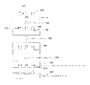
Referring to FIG. 1, a cross-sectional schematic view of a method
of fabricating a perforated thin-film comprising micro/nano structure
perforations
on a substrate surface is illustrated, according to an embodiment of the
present
invention. In one such embodiment, the selective template removal method
comprises first providing a micro and/or nano structure template 110 that has
raised structures, such as micro or nano patterned structures 120 on its
surface
130. In one embodiment, the micro/nano structure template can be made using
any suitable micro/nano structure fabrication method, such as according to a
wafer origination process or can be a replica of a master wafer. In one
embodiment, next a thin-film layer 140 with thickness smaller than the height
of
the raised patterned structures 120 is deposited on the surface 130 of the
template 110 in a thin-film deposition step 150. The thin-film layer 140
deposited
may desirably have a strong adhesion to the template 110. The thin-film layer
140 maybe a single layer or a plurality of layers each desirably have a strong
adhesion to the material they are deposited on. Any suitable thin-film
deposition
method capable to provide a strongly adhered thin-film layer 140 on the
template
110 may be applied, such as a physical vapor deposition or other suitable
method that results in formation of micro or nano-structures, such as thin
film
caps or "islands" 160. In an embodiment, the thin-film caps 160 have an
overhang 170. In an embodiment, each of the overhangs are sized desirably at
least a little larger than the raised structures 120 of the template substrate
110,
and in some embodiments, resemble such "mushroom" shaped overhanging
thin-film caps.
In one embodiment, the thin-film coated template 110 is then
further coated by a thick curable potting material 180 in a potting material
coating
step 190 that when hardened or cured will exhibit poor adhesion to the
deposited
thin-film layer 140. The thickness of the potting material is larger than the
height
of the raised patterned structures 120. The curable potting material can be
any
suitable curable resin and/or polymer potting material, may in one aspect
desirably provide for being hardened using standard time, thermal and/or UV
curing techniques, for example. In one embodiment, the hardened potting
{00062201} 14
- --
CA 3014989 2019-06-28
material 180 may desirably surround and encapsulate (such as by mechanically
interlocking or "grabbing" the 3D shape of) the thin-film caps 160 of the thin-
film
material.
In one aspect, a selective template removal (maybe named
"template snatching") step 200 may desirably mechanically separate the
hardened potting material (such as a UV cured resin or polymer for example)
180
from the template 110, so as to desirably leave the coated thin-film layer 140
adhered to the flat surface 130 as the thin-film layer 140 preferentially
adheres
more strongly to the template 110 than to the potting material 180 coated over
the thin-film layer 140. In a particular embodiment, the same mechanical
selective template removal step 200 desirably also selectively removes or
"snatches" the overhanging thin-film caps 160 from the template 110 as the
thin-
film caps 160 (or "island-like" portions of the thin-film layer coated on a
top
portion of each of the plurality of raised structures) are encapsulated or
mechanically interlocked within corresponding cavities in the hardened potting
material 180.
In one embodiment, such selective template removal step 200 may
desirably result in two micro/nano structure devices. In one aspect, the first
such
device may comprise a micro/nano structure patterned perforated thin-film 210
comprising a plurality of micro/nano structure perforations. In an embodiment,
each of the plurality of micro-/nano-structure perforations correspond to the
location of each of the plurality of raised structures 120 of the template
110. The
second such device may comprise a hardened potting material layer 180
comprising a plurality of precisely shaped and positioned nano/micro structure
particles 220 (comprising the selectively removed overhanging thin-film caps
160) encapsulated within the hardened potting material layer 180.
In one such embodiment, both micro/nano structure devices can be
used in many applications, such as, for example: plasmonic devices,
metamaterial devices, membranes (e.g. in separation, fuel cells, liquid
filters, gas
filters, and others), optical filters, textured electrical electrodes,
patterned
contacts, patterned electronic/optical circuits, sensors (e.g. bio-sensors,
gas
{00062201} 15
_____________________________________________ _ -
CA 3014989 2019-06-28
detectors, refractive index sensors, fluid sensors, molecule detectors, and
others), optical polarizers, displays (in devices like televisions, monitors,
cell-
phones, laptops, wearable electronics, and others), and document security
features, for example.
A first variation of the selective template removal (Le. template
snatching) is illustrated in FIG. 2. The process steps are substantially like
that of
FIG. 1. However, the thin-film caps 160 are strongly adhered to the surface
120
of the template 110 such that the mechanical separation 200 (or template
snatching) of the hardened potting material 180 from the template 110 results
in
breaking and separating each of the raised structures 120 from the surface 130
of the template 110 together with the thin-film caps 160. In spite of this
minor
difference, the products of this process can be substantially similar to that
of FIG.
1.
A second variation of the selective template removal (i.e. template
snatching) is illustrated in FIG. 3. The process steps are exactly like that
of FIG.
1. However, the thin film deposited on a top portion of each of the raised
structures 120 do not need to form a size larger than the size of the raised
structures themselves. That is, each of the thin-film caps 160 do not require
an
overhang 170 as in the variation shown in FIG. 1. Instead, each of the
plurality of
raised structures 120 are shaped to have an overhanging profile that provides
mechanical means for the potting material 180 to harden and encapsulate them.
Like FIG. 2, here the mechanical separation of the hardened potting material
180
from the template 110 results in breaking and separating of each of the
plurality
of raised structures 120 from the surface 130 of the template 110 together
with
the thin-film caps 160. In spite of this minor difference, the end products of
this
process are substantially similar as that of FIG. 1 and FIG. 2.
FIG. 4 illustrates another embodiment of the selective template
removal (i.e. template snatching). The template 110 is layered or covered with
a
first thin-film layer 240 which upon application of the first template
snatching step
200 yields a first perforated thin-film 250 over the template 110. The first
perforated thin-film 250 is then covered again with a second or subsequent
thin-
{00062201} 16
CA 3014989 2019-06-28
¨
film layer 260 followed by a second template snatching to produce a second or
subsequent perforated thin-film 260. This process may be repeated in order to
produce multiple layers of perforated thin-films.
As shown, the initial thin-film deposition step 150 may commence
with depositing a first thin-film layer 240 in a thickness smaller than the
height of
the raised structures 120 on the template 110. In addition to the earlier
steps for
fabricating a product having perforated thin-film comprising micro and/or nano-
structure perforations, a second or subsequent thin-film layer 260 of a second
suitable coating material is deposited over the substrate and raised 120 such
that the second thin-film layer 260 is adhered to the first thin-film layer
240 and
forms second or subsequent overhanging thin-film cap 280 on a top portion of
each of the plurality of raised structures 120. In an embodiment, a second or
subsequent layer of a potting material is deposited over the second thin-film
layer
260 and allowed to harden or cure. The hardening or curing of the potting
material is such that the hardened potting material encapsulates the second or
subsequent overhanging thin-film caps 280. The removing of the hardened
potting material reveals a second or subsequent perforated thin-film 260
layered
over the first perforated thin-film, wherein the perforations correspond to
the
locations of each of the plurality of raised structures 120.
FIGS. 5a and 5b illustrate enlarged scanning electron microscope
images of the perforated film formed by the method illustrated in FIG. 2. FIG.
5a
illustrates a perspective electron microscope view of an exemplary thin-film
coated nanostructure template on a template surface comprising raised nano-
structures 290 having a thin-film layer, according to an embodiment of the
present invention. FIG. 5b illustrates a perspective electron microscope view
of
an exemplary perforated thin-film layer on a template surface 130 comprising
nano-structure perforations 300 following selective removal of thin-film
coated
caps from raised nanostructures, according to another embodiment.
FIG. 6 shows a scanning electron microscope image of the result of
a template snatching process. Here, a thin-film layer, such as 30nm of
aluminum,
was deposited on a template having a periodic arrangement of nano-structures,
{00062201} 17
to....-46
CA 3014989 2019-06-28
such as nano-pillars, on its surface (see left side FIG. 6). The template was
made through a master wafer origination and nano-imprint lithography.
Snatching the aluminum layer deposited on the nano-pillar template using a
hard
UV cured resin resulted in a perforated aluminum thin-film left on the
template
(see right side FIG. 6).
In a further embodiment, the template used in the above described
methods of selective template removal may comprise an original micro/nano
structured template wafer that has gone through all the fabrication steps, or
a
replica of a master wafer replicated with known methods including nanoimprint
lithography. In an embodiment where nano-imprint lithography is used, a
suitable nano-imprint lithographical method may be applied, such as for
example
plate to plate, plate to roll, or roll-to-roll methods. In embodiments, the
template
or master wafer may be made by optical lithography, electron-beam lithography,
focused-ion-beam, laser interference, or a recipe of any other suitable micro-
or
nano-fabrication techniques.
In an embodiment, the template material maybe semiconductor,
glass, quarts, resin, plastic, metal or other suitable materials, and can
include
arbitrary shaped features with sizes less than lOpm.
Although the figures herein illustrated a single pattern, in an
embodiment, the template can comprise a single or a plurality of patterns of
different shapes, sizes, and heights.
In an embodiment, the template may or may not be treated with
adhesion control layers before deposition of the thin-film material to assist
in
adhesion of the thin-film layer on the substrate surface.
In an embodiment, the template may contain both raised and
lowered micro/nano-structures, such as peaks and valleys. The thin-film
material
deposited on top portions of each of the plurality of raised structures (i.e.
apexes)
will be removed by template snatching. The material left in the valleys will
be left
on the template and may provide additional functionality to the final device.
In embodiments, the material of the thin-film layer deposited can be
metals like silver, aluminum, gold, copper, titanium; or dielectrics like
SiO2, TiO2,
100062201} 18
CA 3014989 2019-06-28
õ.
Nb2O5; or semiconductors like Si; or any material with strong adhesion to the
surface of the template, and the deposition method may be physical vapor
deposition or any other method suitable to deposit thin-film with the
characteristics demanded by the application.
In one embodiment, for each selective template removal or
template snatching step, a single layer or multiple layers of the thin-film
material
may be deposited.
In one embodiment, the resin can be thermally cured, UV cured,
molten plastic, or anything that satisfies the hardness and adhesion
properties
needed.
In one embodiment, the selective template removal or template
snatching process may be implemented in roll to roll, plate to plate, or plate
to roll
format, either manually or through design/use of appropriate machinery.
In one embodiment, the devices of the template snatching may be
further processed by deposition of more layers and/or etching steps and/or
other
micro/nano fabrication steps to yield the final devices.
In one embodiment, the final product may be used as an etch mask
or on optical mask to manufacture further products and devices.
In one embodiment, the selective template removal, or template
snatching process may be repeated more than once to yield multiple layers of
nano or microstructure thin-film layers.
In one embodiment, the final micro/nano structured devices
resulting from the above-described selective template removal methods may
comprise plasmonic devices, metamaterials, including thin-film colour shifting
devices useful to function as optically variable devices for document
security.
In one embodiment, the final devices may comprise plasmonic or
metamaterials devices useful to generate structural colors such as for
environmentally friendly die-free prints. In one embodiment, the final devices
may be used as an optical polarizer and/or optical filter. In one embodiment,
the
final devices may function as sensors for refractive index, fluids, gasses,
molecules, bio-materials, and others. In one embodiment, the final devices may
{00062201} 19
CA 3014989 2019-06-28
õ _
=
be used as membranes in separation, fuel cells, liquid or gas filters, and
others.
In one embodiment, the final devices may be used in construction of displays
or
devices like TVs, monitors, cell-phones, laptops, wearable electronics, and
others.
In one aspect, the template of micro-/nano-structures may comprise
substantially micro-/nano-structure features, such as micro-/nano-cylinders,
or
micro-/nano-cuboids or grooves, for example. In further aspects of the present
invention, the original micro-/nano-structures according to the above
described
methods may comprise at least one of: multiple periodic arrays of micro-/nano-
structures comprising different micro-/nano-structure dimensions and/or array
periodicities and/or array types (i.e. rectangular, hexagonal, and other
geometrical arrays); non-periodic or periodic arrays of micro-/nano-structures
comprising different micro-/nano-structure dimensions arranged in arbitrary
positions; multiple combinations of different arrays of different micro-/nano-
structures; multiple arrays of different configurations or shapes of micro-
/nano-
structures such as one or more of micro-/nano-pillars or columns, micro-/nano-
cones, micro-Mono-wires, micro-/nano-domes, micro-/nano-ridges, micro-/nano-
pyramids, micro-/nano-holes, elongated micro-/nano-holes, micro-/nano-slots
and micro-/nano-grooves, for example. In yet a further embodiment of the
present invention, the original micro-/nano-structures according to the above
described methods may comprise any desired combination, geometries or
configurations of 2D (such as in-plane) and/or 3D (such as out of plane) micro-
/nano-structures and/or grids or arrays thereof on the surface of the template
substrate.
The above description of exemplary embodiments of the present
invention, including what is described in the Abstract, is not intended to be
exhaustive or to limit the embodiments of the invention to the precise forms
disclosed above. Although specific embodiments and examples are described
herein for illustrative purposes and to allow others skilled in the art to
comprehend their teachings, various equivalent modifications may be made
{00062201} 20
_
CA 3014989 2019-06-28
without departing from the scope of the disclosure, as will be recognized by
those
skilled in the relevant art.
{00062201} 21
CA 3014989 2019-06-28