Note : Les descriptions sont présentées dans la langue officielle dans laquelle elles ont été soumises.
CA 03015216 2018-08-21
WO 2017/143442
PCT/CA2017/050228
TILEABLE BLOCK DETECTORS FOR SEAMLESS BLOCK DETECTOR ARRAYS IN
POSITRON EMISSION MAMMOGRAPHY
CROSS-REFERENCE TO RELATED APPLICATIONS
100011 This
application claims the benefit of, and herein incorporates by
reference in its entirety, U.S. Provisional Patent Application Serial No.
62/300,256, filed
on February 26, 2016, and entitled "TILEABLE BLOCK DETECTORS FOR SEAMLESS
BLOCK DETECTOR ARRAYS IN POSITRON EMISSION MAMMOGRAPHY."
BACKGROUND
100021 The
field of the present disclosure is positron emission tomography
("PET"). More particularly, the present disclosure relates to radiation
detector arrays
for use in PET systems, including positron emission mammography ("PEM")
systems.
100031 Women
with highly dense breast tissue suffer from both higher risk of
breast cancer and lower sensitivity of mammographic screening. PEM offers a
potential
solution for these women who have an increased need for effective screening.
If the
radiotracer dose is lowered sufficiently, PEM could be an effective screening
tool,
especially in high-risk women with dense breasts for whom mammography has
unacceptably low sensitivity. Currently, a PEM dose of 370 MBq (10 mCi) of
fludeoxyglucose ("FDG") has a lifetime equivalent risk that is 23 times
greater than
digital mammography, which severely limits its clinical acceptance.
100041 Thus,
there is a need to provide a PEM system that is capable of
generating images using a significantly reduced dose administered to the
subject while
maintaining high sensitivity and specificity in a screening context.
100051 In some
PEM systems, one or more large block detectors are scanned over
the subject's breast. Although these systems may be able to operate at lower
dose to the
subject, the scanning technique reduces the amount of time that the sensors
are
-1-
CA 03015216 2018-08-21
WO 2017/143442
PCT/CA2017/050228
exposed to a particular breast region, thereby reducing the sensitivity of the
system. It is
also possible for other measurement errors to be introduced because of the
scanning
motion.
100061 Other
PEM systems use a circular array of gamma ray detectors. In these
systems, the subject lies prone and the breast hangs into the ring of the
array. The ring
design allows for greater sensitivity and faster scanning times, but is less
able to
accommodate differences in breast sizes compared to other systems and has
poorer
imaging of lesions near the chest wall.
100071 It
would be desirable to have a PEM system that uses a detector that is
large enough to cover the entire breast with slight compression and without
needing to
move the detector. Such a stationary system would be able to collect more
signal while
using a lower radio-tracer dose.
SUMMARY OF THE DISCLOSURE
100081 The
present disclosure addresses the aforementioned drawbacks by
providing a block detector for use in a positron emission tomography ("PET")
system.
The block detector includes a scintillator array comprising a plurality of
scintillator
crystals, a photodetector comprising a plurality of photodetector elements,
and a light
guide that is optically coupled to the scintillator array and the
photodetector. The
photodetector has a surface area smaller than a surface area of the
scintillator array
such that the scintillator array defines an overhang relative to the
photodetector. The
light guide has a first surface facing and optically coupled to a bottom
surface of the
scintillator array, and a second surface facing and optically coupled to an
active surface
of the photodetector. The first surface of the light guide has a first surface
area and the
second surface of the light guide has a second surface area that is smaller
than the first
-2-
CA 03015216 2018-08-21
WO 2017/143442
PCT/CA2017/050228
surface area.
100091 It is another aspect of the present disclosure to provide an array
of block
detectors for use in a PET system. The array of block detectors includes a
plurality of
block detectors, where each block detector includes a scintillator array
comprising a
plurality of scintillator crystals, a photodetector comprising a plurality of
photodetector
elements, and a light guide that is optically coupled to the scintillator
array and the
photodetector. The photodetector has a surface area smaller than a surface
area of the
scintillator array such that the scintillator array defines an overhang
relative to the
photodetector. The light guide has a first surface facing and optically
coupled to a
bottom surface of the scintillator array, and a second surface facing and
optically
coupled to an active surface of the photodetector. The plurality of block
detectors are
arranged in an array such that the scintillator arrays in adjacent block
detectors meet at
an interface with substantially no gap therebetween and photodetectors in
adjacent
block detectors are separated by a gap defined by the overhang.
100101 The foregoing and other aspects and advantages of the present
disclosure
will appear from the following description. In the description, reference is
made to the
accompanying drawings that form a part hereof, and in which there is shown by
way of
illustration a preferred embodiment. This embodiment does not necessarily
represent
the full scope of the invention, however, and reference is therefore made to
the claims
and herein for interpreting the scope of the invention.
BRIEF DESCRIPTION OF THE DRAWINGS
100111 FIG. 1 is an exploded view of an example four-way tileable block
detector.
100121 FIG. 2 is a side view of an example four-way tileable block
detector.
100131 FIG. 3 shows a seamless array of four-way tileable block detectors.
-3-
CA 03015216 2018-08-21
WO 2017/143442
PCT/CA2017/050228
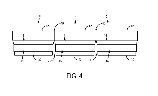
100141 FIG. 4
is a cross-sectional view of the seamless array of four-way tileable
block detectors of FIG. 3.
DETAILED DESCRIPTION
100151
Described here are tileable block detectors for use in nuclear medicine
applications, such as in positron emission tomography ("PET") systems, and in
some
specific examples positron emission mammography ("PEM") systems. The tileable
block
detectors are one component in such PET or PEM systems. Advantageously, the
block
detectors described here are four-side tileable such that seamless arrays of
block
detectors can be constructed for use in PET or PEM systems. When so arrayed,
the block
detectors allow for a full-size seamless detector that achieves full coverage
of an object
(e.g., a gently immobilized breast), improves data collection, and enables
high-
resolution imaging with a significantly lower radiation dose than with other
currently
available PEM systems.
100161 PET
systems often utilize block detectors to detect gamma rays. These
block detectors include a photodetector (e.g., photomultiplier tubes (PMTs) or
solid-
state photodetectors) that is optically coupled to a scintillator, such as a
scintillating
crystal. PET block detectors use a light sharing technique to define the
position where
gamma rays interacted with the scintillator more efficiently and precisely.
For instance,
to achieve better spatial resolution, an array of scintillator crystals (e.g.,
a pixelated
scintillating crystal) is used. Such arrays of scintillator crystals are
optically coupled to
the photodetector through a light guide to distribute light to an array of
photodetectors.
100171 The
block detectors described here are designed to eliminate gaps
between adjacent detectors when they are arrayed into larger structures, such
as 3x3
arrays, 4 X 4 arrays, 3x4 arrays, and so on. When block detectors using solid-
state
-4-
CA 03015216 2018-08-21
WO 2017/143442
PCT/CA2017/050228
photodetectors are arrayed, it is a common problem to have gaps between the
scintillators in the block detectors. The block detectors described here are
designed to
address and overcome this problem.
100181 FIGS. 1
and 2 show an example of a tileable block detector 10 for use in
PET systems, including PEM systems. Each block detector 10 generally includes
a
scintillator array 12, a light guide 14, and a photodetector 16. Preferably,
the
photodetector 16 is a solid-state photodetector having an array of
photodetector
elements, or pixels. Example solid-state photodetectors include silicon
photomultiplier
("SiPM"), avalanche photodiodes ("APD"), and digital SiPM without light
guides.
Advantageously, the block detector 10 is designed to be a four-way tileable
detector,
such that seamless arrays of block detectors 10 can be constructed, including
3x3
arrays, 4 x 4 arrays, 3x 4 arrays, and so on.
100191 In
general, the block detector 10 is constructed such that the scintillator
array 12 has a larger surface area than the light guide 14, photodetector 16,
and front
end electronics 32 coupled to the photodetector 16. Thus, the surface area of
the block
detector 10 is defined by the size of the scintillator array 12 used. More
particularly, the
scintillator array 12 is dimensioned to define an overhang 34 over the
photodetector
16, which allows the block detectors 10 to be seamlessly tileable. As one
example, the
overhang 34 can be about 500-600 nm. In some embodiments, the overall
thickness of
the block detector 10 is about 35 mm or less, which allows the block detector
10 to be
placed very close to the chest wall such that images of the chest can be
acquired to
detect lesions therein.
100201 The
scintillator array 12 generally comprises an array of scintillator
crystals 18. The scintillator array 12 can be constructed as a cut-block
scintillator, or as
a reflector-block scintillator. As one example, the scintillator crystals 18
can be LYSO:Ce
-5-
CA 03015216 2018-08-21
WO 2017/143442
PCT/CA2017/050228
crystals; however, other inorganic crystals can also be used, including
crystals
composed of CsF, NaI(T1), LaC13(Ce), BGO, CaF2(Eu), YAG(Ce), and so on. In
some other
embodiments, the scintillator crystals 18 can be organic or ceramic crystals.
In still
other embodiments, the scintillator array 12 can include arrays of other non-
crystal
scintillators, including those based on organic liquids, or fluorescent
emitters.
100211 The
scintillator array 12 extends from a top surface 20 to a bottom
surface 22. The light guide 14 is positioned between the scintillator array 12
and the
photodetector 16 so as to optically couple the scintillator array 12 to the
photodetector
16. Radiation (e.g., 511 keV photons) impinging on the top surface 20 of the
scintillator
array 12 is absorbed by the scintillator array 12, in response to which light
(e.g., visible
light) is emitted from the scintillator array 12. The emitted light is
transmitted to the
photodetector 16 by way of the light guide 14.
100221 The
light guide 14 has a first surface 24 facing and optically coupled to the
bottom surface 22 of the scintillator array 12, and a second surface 26 facing
and
optically coupled to an active surface 28 of the photodetector 16. Preferably,
the light
guide 14 is dimensioned such that the first surface 24 has the same surface
area as the
bottom surface 22, and the second surface 26 has the same surface area as the
active
surface 28 of the photodetector 16. The light guide 14 can be composed of any
suitable
type of glass (e.g., borosilicate, fused silica, lead glass) as well as any
suitable
transparent plastic (e.g., acrylic, polycarbonate, polystyrol), and can be
constructed
using an accurate repeatable polishing or thermal etching technique to
maintain high
quality of the light guide.
100231 Light
impinging on the first surface 24 of the light guide is distributed
from one pixel (e.g., the crystal 18 from which the light was emitted) of the
scintillator
array 12 between many pixels of the photodetector 16. Using the light guide 14
thus
-6-
CA 03015216 2018-08-21
WO 2017/143442
PCT/CA2017/050228
allows for fewer electronic readout channels while at the same time yielding
very
accurate results in determining the position where incident radiation (e.g.,
511 keV
photons) hit the scintillator array 12. Furthermore, by keeping the surface
area of the
first surface 24 large, the light guide 14 allows the block detector 10 to
maintain the
same level of photodetection efficiency as in the case of no overhang 34
existing
between the scintillator array 12 and the photodetector 16.
100241 The
light guide 14 is also generally shaped so its first surface 24 has a
larger surface area than the surface area of the second surface 26 of the
light guide 14.
In some embodiments, the edges 30 of the light guide 14 are beveled to slope
inward
from the first surface 24 to the second surface 26 of the light guide 14. As
other
examples, the edges 30 of the light guide can be generally convex or concave.
Preferably,
the edges 30 are coated with a reflective compound to prevent scintillation
light loss
and maintain high light collection efficiency. Whenever a gamma ray from
positron
annihilation interacts with the scintillator array 12 near the edge of the
scintillator
array 12, this reflective coating directs most of the light to the
photodetector 16.
100251 Light
emitted by the scintillator array 12 and impinging on the
photodetector 16 by way of the light guide 14 creates electrical signals that
are readout
as data from the photodetector 16 by front-end electronics 32. This data is
communicated to a computer system for image reconstruction and other
processing. As
mentioned above, the block detector 10 provides better spatial resolution by
using a
scintillator array 12 that includes an array of scintillating crystals 18 and
a
photodetector 16 that includes an array of photodetector elements. In this
configuration, the light guide 14 distributes the light emitted from a
scintillator crystal
18 in the scintillator array 12 to the array of photodetector elements. Anger
logic math
can then be used to determine the position of gamma ray interactions with the
-7-
CA 03015216 2018-08-21
WO 2017/143442
PCT/CA2017/050228
scintillator array 12.
100261 An
example array 36 of block detectors 10 is shown in FIG. 3 with a
corresponding cross-section of the array 36 shown in FIG. 4. Because the block
detectors 10 can be seamlessly tiled, the block detector array 36 provides an
imaging
zone with virtually no dead zones between the block detectors 10. As a result
of this
seamless construction, less radiation will escape the block detector array 36
due to gaps
that are present between block detectors in other currently available devices.
Although
a 3x3 array is illustrated in FIG. 2, because the block detectors 10 are four-
way
tileable, any suitable configuration of arrayed block detectors 10 can be
constructed,
including 3x4 arrays, 4 X 4 arrays, and so on.
100271 As one
example, each block detector 10 can have dimensions of 57.66 mm
by 57.66 mm (i.e., the scintillator array 12 is dimensioned to be 57.66 mm by
57.66
mm), such that a 3x3 array 36 of block detectors 10 would have an imaging zone
of
17.3 cm by 17.3 cm. It will be appreciated by those skilled in the art,
however, that
different sized block detectors 10 can also be constructed.
100281 When
arrayed, the overhang 34 of the block detectors 10 define a gap 38
between the photodetectors 16 in adjacent block detectors 10, while allowing a
seamless interface 40 between the scintillator arrays 12 in adjacent block
detectors 10.
Advantageously, the gap 38 between photodetectors 16 can act as a convective
channel
that allows airflow around the photodetectors 16 and front end electronics 32,
thereby
providing cooling of these electronic components of the block detector 10. As
mentioned above, the overhang 34 is generally dimensioned to be about 500-600
nm
and, thus, the gap 38 between photodetectors 16 is about 1000-1200 nm.
100291 The present disclosure has described one or more preferred
embodiments, and it should be appreciated that many equivalents, alternatives,
-8-
CA 03015216 2018-08-21
WO 2017/143442
PCT/CA2017/050228
variations, and modifications, aside from those expressly stated, are possible
and within
the scope of the invention.
-9-