Note : Les descriptions sont présentées dans la langue officielle dans laquelle elles ont été soumises.
THERMOELECTRIC PIEZOELECTRIC GENERATOR
FIELD
The present invention relates to electric generators and, in particular, to
electric
generators integrating flexible thermoelectric and piezoelectric components
into a single device
architecture.
BACKGROUND
Thermoelectric and piezoelectric generators are generally incompatible because
each uses
a vastly different method to couple to their respective energy sources. For
example, when a
thermoelectric generator ('1EG) is exposed to a thermal gradient, a voltage is
generated due to
the Seebeck effect. When each thermoelectric element maintains the maximum
thermal gradient,
the l'EG achieves optimal performance. Alternatively, since mechanical
deformation of a
piezoelectric material creates a potential between the generated bound surface
charge,
piezoelectric generators (PEG) need to mechanically couple to dynamic systems
to harvest
energy. Due to this mismatch between heat and mechanical source coupling, TEGs
are typically
designed to be rigid and static while PEGs are flexible and dynamic making
them incompatible
with one another, even though the main target systems exhibit both waste
thermal and
mechanical energy.
In addition to the different coupling mechanisms, TEGs and PEGs are
destructive to one
another because of the mismatch in voltage signal. Under static thermal
gradients, TEGs
generate DC voltages and are essentially low value resistive elements.
Alternatively, dielectric
1
Date Recue/Date Received 2022-07-28
of these elements negates the power production of the other, depending on
arrangement. For
example, by placing a TEG and PEG electrically in parallel, the low resistance
TEG will
discharge the PEG capacitor thereby causing only the TEG to generate power.
Alternatively, if
the TEG and PEG are placed electrically in series, the capacitor creates an
open circuit
dramatically decreasing the power output of the TEG.
US2012/133210discloses an electric generator comprising a thermoelectric layer
and a
piezoelectric layer.
SUMMARY
In view of these technical problems and incompatibilities, electric generators
are
described herein which efficiently integrate thermoelectric and piezoelectric
components into a
single device architecture. Briefly, an electric generator described herein
comprises a
thermoelectric film having a plurality of lateral p-n junctions across a face
of the film, the lateral
p-n junctions established at interfaces between p-type regions and n-type
regions and the p-type
regions comprise electrically conductive particles dispersed in or on a first
carrier and the n-type
regions comprise electrically conductive particles dispersed in or on a second
carrier. A
piezoelectric film is coupled to the thermoelectric film and an electrode is
coupled to the
piezoelectric film. In some embodiments, the electric generator adopts a
sandwich structure
wherein the piezoelectric film is positioned between the thermoelectric film
and electrode.
Further, the thermoelectric film can be folded at the p-n junctions. In such
embodiments, the
electric generator can have a corrugated structure or orientation.
These and other embodiments are described further in the following detailed
description.
BRII-T DESCRIPTION OF THE DRAWINGS
FIG. 1(a) illustrates construction of an electric generator according to some
embodiments
described herein.
FIG. 1(b) illustrates an electric generator in a folded or corrugated
orientation according
to some embodiments described herein.
FIG. 2(a) illustrates thermoelectric voltage generated by an electric
generator described
herein compared with the theoretic maximum based on intrinsic thermoelectric
values.
FIG. 2(b) illustrates thermal power generated by a 2x2 array of electric
generators
described herein with internal load matching compared to the theoretical
maximum.
2
Date Recue/Date Received 2022-03-09
CA 03016893 2018-09-06
WO 2017/156296 PCT/US20171021613
FIG. 3(a) illustrates voltage generated by a single electric generator while
undergoing
harmonic stress according to some embodiments.
FIG. 3(b) illustrates the ratio between the measured peak-to-peak voltage and
input stress
according to some embodiments.
DETAILED DESCRIPTION
Embodiments described herein can be understood more readily by reference to
the
following detailed description and examples and their previous and following
descriptions.
Elements, apparatus and methods described herein, however, are not limited to
the specific
embodiments presented in the detailed description and examples. It should be
recognized that
these embodiments are merely illustrative of the principles of the present
invention. Numerous
modifications and adaptations will be readily apparent to those of skill in
the art without
departing from the spirit and scope of the invention.
Electric generators are described herein integrating thermoelectric and
piezoelectric
components. In some embodiments, an electric generator comprises a
thermoelectric film having
a plurality of lateral p-n junctions across a face of the film, the lateral p-
n junctions established at
interfaces between p-type regions and n-type regions. A piezoelectric film is
coupled to the
thermoelectric fihn and an electrode is coupled to the piezoelectric film.
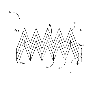
FIGS. 1(a)-(b) illustrate
an electric generator according to some embodiments described herein. As
illustrated in FIG.
1(a), a piezoelectric film or layer 12 is coupled to a thermoelectric film or
layer 11. The
thermoelectric film 11 includes a plurality of lateral p-n junction across the
film 11. An
electrode 13 is coupled to the piezoelectric film. Referring now to FIG. 1(b),
the thermoelectric
film 11 can be folded at the p-n junctions 14, placing the electric generator
10 in a corrugated
orientation. Folding the thermoelectric film 11 and associated piezoelectric
film 12 and
electrode 13 allows for a thermal gradient (Al) to be established across the
thickness of the
electric generator 10. Thermoelectric voltage is measured between the opposite
sides of the
electrode 13, and piezoelectric voltage is measured between the electrode 13
and thermoelectric
film 11. In the embodiment of FIG. 1(b), the thermoelectric film 11 can serve
as an electrode
that provides a capacitive structure with the back electrode 13 for extracting
piezoelectric voltage
resulting from mechanical deformation of the piezoelectric film 12.
3
CA 03016893 2018-09-06
WO 2017/156296 PCT/US2017/021613
Turning now to specific components, the electric generator comprises a
thermoelectric
film or layer having a plurality of lateral p-n junctions across a face of the
film, the lateral p-n
junctions established at interfaces between p-type regions and n-type regions.
The p-type
regions and n-type regions can be formed of any materials not inconsistent
with the objectives of
the present invention. As detailed further herein, the p-type regions and n-
type regions can
comprise organic materials, inorganic materials or various combinations
thereof.
In some embodiments, the p-type regions comprise conductive particles
dispersed in or
on a first carrier. Electrically conductive particles of the p-type regions
can include p-type
organic nanoparticles, p-type inorganic nanoparticles or mixtures thereof. In
some embodiments,
p-type nanoparticles are selected from the group consisting of nanotubes,
nanowires, nanorods,
platelets and sheets. The p-type nanoparticles can have a 1-dimensional or 2-
dimensional
structure, in some embodiments.
P-type organic nanoparticles can include carbon nanotubes, fullerenes,
graphene or
mixtures thereof. In some embodiments, lattice structures of the organic p-
type nanoparticles
include one or more dopants such as boron. Alternatively, p-type dopant is
externally applied to
the organic nanoparticles by the environment surrounding the nanoparticles in
the first carrier.
For example, the first carrier can provide p-dopant to surfaces of the organic
nanoparticles.
Similarly, one or more p-dopant species can be dispersed in the first carrier
for interaction with
the organic nanoparticles.
P-type inorganic nanoparticles can include binary, ternary and quaternary
semiconductor
compositions formed from elements selected from Groups IB, JIB and IIIA-VIA of
the Periodic
Table. For example, p-type inorganic nanoparticles can be formed of Cu2Te,
Cu2.õSe, Sb2Te3,
Ag2Se, Ag2Te, Cu2Te, Cu2Se, Se or Te. P-type inorganic nanoparticles can also
be selected from
various transition metal dichalcogenides, MX2, where M is a transition metal
and X is a
chalcogen. Table I provides non-limiting examples of p-type inorganic
nanoparticles and
morphology.
Table 1¨ P-type Inorganic Nanoparticles
Nanoparticle Composition Morphology
Cu2,Te Nanowires
Cu2,Se Nanoveires
Sb2'le3 Nanoplatelets
Te Nanorods
4
CA 03016893 2018-09-06
WO 2017/156296
PCTAIS2017/021613
Ag2Se ID Nanowire
Ag2Te ID Nanowire
Cu2Te ID Nanowire
Cu2Se ID Nanowirc
Sc 1D Nanowire
Te ID Nanowire
In some embodiments, p-dopant is externally applied to inorganic nanoparticles
by the first
carrier and/or one or more p-dopant species dispersed in the first carrier.
For example, the
inorganic nanoparticles can be sufficiently thin that electronic properties of
the nanoparticles are
dominated by surface behavior and surface interactions. The inorganic
nanoparticles can lack
sufficient thickness to exhibit any meaningful bulk properties. Therefore, p-
dopant species
externally applied to the inorganic nanoparticles can create the p-type
character of the
nanoparticles. In some embodiments, the inorganic nanoparticles of the p-type
region are one or
more topological insulators.
P-type organic nanoparticles and/or inorganic nanoparticles can be present in
the first
carrier in any amount not inconsistent with the objectives of the present
invention. In some
embodiments, p-type organic and/or inorganic nanoparticles are present in the
first carrier in an
amount of 0.1 weight percent to 30 weight percent. In some alternative
embodiments, a layer of
the p-type nanoparticles is formed over the first carrier. In such
embodiments, the first carrier
serves as a support for the nanoparticle layer as opposed to a matrix in which
the organic and/or
inorganic nanoparticles are dispersed.
The first carrier can be an organic material, inorganic material or
combinations thereof.
For example, the first carrier can comprise one or more polymeric species.
Suitable polymeric
species can include one or more fluoropolymers. In some embodiments, the first
carrier
comprises polyvinylidene fluoride (PVDF), polyvinyl fluoride (PVF),
polyvinylidene fluoride-
tritluoroethylene (PVDF-TrFE), polyvinylidene fluoride-tetrailuorocthylene
(PVDF-TFE),
polytetrafluoroethylene (PTFE), or mixtures or copolymers thereof.
Semicrystalline polymers of
PVDF, PVDF-TFE and/or PVDF-TrFE used in p-type regions of the thin-film layer
can
demonstrate increased amounts of 0-phase. For example, PVDF, PVDF-TFE and/or
PVDF-
TrFE of a p-type layer can display a phase ratio of 0/a of 1.5 to 2.5. In some
embodiments, the
0/a phase ratio is 2 to 2.5. 0-phase crystallites can be provided a non-random
orientation by
5
CA 03016893 2018-09-06
WO 2017/156296 PCT/US2017/021613
poling techniques, thereby enhancing piezoelectric and pyroelectric properties
of the polymeric
matrix.
Alternatively, the first carrier can comprise one or more elastomeric species,
including
polyisoprene, polyisobutylene and polysiloxanes, such as polydirnethylsiloxane
(PDMS). The
first organic carrier can also comprise polyacrylic acid (PAA),
polymethacrylate (PMA),
polymethylmethacrylate (PMMA) or mixtures or copolymers thereof. Additionally,
the first
carrier can comprise polyolefin including, but not limited to polyethylene,
polypropylene,
polybutylene or mixtures or copolymers thereof.
Semiconducting polymers can also find application as the first carrier.
Suitable
semiconducting polymers can include phenylene vinylenes, such as
poly(phenylene vinylene)
and poly(p-phenylene vinylene) (PPV), and derivatives thereof. In some
embodiments,
semiconducting polymers comprise poly fluorenes, naphthalenes, and derivatives
thereof. In
other embodiments, semiconducting polymers comprise poly(2-vinylpyridine) (P2V
P),
polyamides, poly(N-vinylcarbazole) (PVCZ), polypyrrole (PPy), polyaniline
(PAn) and poly[2,6-
(4,4-bis-(2-ethylhexyl)-4H-cyclopenta[2,1-b;3,4-tidithiophene)-alt-4,7-(2,1,3-
benzothiadiazole)] (PCPDTBT).
Alternatively, in some embodiments, the first carrier is an inorganic carrier.
Inorganic
carriers, in some embodiments, include polycrystalline ceramics or other
particulate inorganic
materials.
N-type regions of the thermoelectric film can comprise conductive particles
dispersed in
or on a second carrier. Electrically conductive particles of the n-type
regions can include n-type
organic nanoparticles, n-type inorganic nanoparticles or mixtures thereof. In
some embodiments,
n-type nanoparticles are selected from the group consisting of nanotubes,
nanowires, nanorods,
platelets and sheets. The n-type nanoparticles can have a 1-dimensional or 2-
dimensional
structure, in some embodiments.
N-type organic nanoparticles can include carbon nanotubes, fullerencs,
graphene or
mixtures thereof. In some embodiments, lattice structures of the organic n-
type nanoparticles
include one or more dopants such as nitrogen. Alternatively, n-type dopant is
externally applied
to the organic nanoparticles by the environment surrounding the nanoparticles
in the second
carrier. For example, the second carrier can provide n-dopant to surfaces of
the organic
6
CA 03016893 2018-09-06
WO 2017/156296 PCT/US2017/021613
nanoparticles. Similarly, one or more n-dopant species, such as
polyethyleneimine (PEI), can be
dispersed in the second carrier for interaction with the organic
nanoparticles.
N-type inorganic nanoparticles can include binary, ternary and quaternary
semiconductors compositions formed from elements selected from Groups IB, [TB
and II IA-VIA
of the Periodic Table. For example, n-type inorganic nanoparticles can be
formed of Bi2Se3,
Bi2Te3, Bi2Te3-xSex, Sb2Te3, Sb2,BixTe3, Cu doped Bi2Se3 and Ag surface
modified Bi2Se3 and
Bi2Te3 N-type inorganic nanoparticles can also be selected from various
transition metal
dichalcogenides, MX2. In some embodiments, n-type transition metal
dichalcogenides include
T1S2, WS2 and MoS2. Table 11 provides non-limiting examples of n-type
inorganic nanoparticles
and morphology.
Table 11 -- N-type inorganic Nanoparticles
Nanoparticle Composition Morphology
Cu doped Bi2Se3 Platelets
Bi2Se3 2D plate
Bi2Te3 213 plate
Bi2Te3_õSe, 213 plate
Sb2Te3 213 plate
Sb2_õ13i, l'e3 213 plate
TiS2 213 plate
WS2 2D plate
MoS2 2D plate
In some embodiments, n-dopant is externally applied to inorganic nanoparticles
by the second
carrier and/or one or more n-dopant species dispersed in the first organic
carrier. As with the p-
type inorganic nanoparticles, the n-type inorganic nanoparticles can lack
sufficient thickness to
exhibit any meaningful bulk properties. Therefore, n-dopant species externally
applied to the
inorganic nanoparticles can create the n-type character of the nanoparticles.
Moreover, the
inorganic nanoparticles of the n-type region can be selected from one or more
topological
insulators.
N-type organic nanoparticles and/or inorganic nanoparticles can be present in
the second
carrier in any amount not inconsistent with the objectives of the present
invention. In some
embodiments, n-type organic and/or inorganic nanoparticles are present in the
second carrier in
an amount of 0.1 weight percent to 30 weight percent. In some alternative
embodiments, a layer
of the n-type nanoparticles is formed over the second carrier. In such
embodiments, the second
7
CA 03016893 2018-09-06
-
WO 2017/156296 PCT/US2017/021613
carrier serves as a support for the nanoparticle layer as opposed to a matrix
in which the organic
and/or inorganic nanoparticles arc dispersed.
The second carrier can be an organic material, inorganic material or
combinations
thereof. The second carrier can comprise any material operable to host or
support n-type organic
nanoparticles and/or n-type inorganic nanoparticles to provide a thin-film
structure having n-type
electronic structure. For example, the second carrier can comprise one or more
polymeric
species. Suitable polymeric species can include one or more fluoropolymers. In
some
embodiments, the second organic carrier comprises polyvinylidene fluoride
(PVDF), polyvinyl
fluoride (PVF), polyvinylidene fluoride-trifluoroethylene (PVDF-TrFE),
polyvinylidene
fluoride-tetrafluoroethylene (PVDF-TFE), polytetrafluoroethylene (PTFE), or
mixtures or
copolymers thereof. Semicrystalline polymers of PVDF, PVDF-TFE and/or PVDF-
TrFE used in
n-type regions of the thin-film layer can demonstrate increased amounts of 0-
phase. For
example, PVDF, PVDF-TFE and/or PVDF-TrFE of a p-type layer can display a phase
ratio of
0/a. of 1.5 to 2.5. In some embodiments, the 13/u phase ratio is 2 to 2.5.
Alternatively, the second organic carrier can comprise one or more elastomeric
species,
including polyisoprcne, polyisobutylene and polysiloxanes, such as
polydimethylsiloxane
(PDMS). The second organic carrier can also comprise polyacrylic acid (PAA),
polymethacrylate (PMA), polymethylmethacrylate (PMMA) or mixtures or
copolymers thereof.
Additionally, the second organic carrier can comprise polyolefin including,
but not limited to
polyethylene, polypropylene, polybutylene or mixtures or copolymers thereof
Semiconducting polymers can also find application as the second organic
carrier.
Suitable semiconducting polymers can include phenylene vinylenes, such as
poly(phenylene
vinylene) and poly(p-phenylene vinylene) (PPV), and derivatives thereof. In
some
embodiments, semiconducting polymers comprise poly fluorenes, naphthalenes,
and derivatives
thereof. In other embodiments, semiconducting polymers comprise poly(2-
vinylpyridine)
(P2VP), polyarnides, poly(N-vinylcarbazole) (PVCZ), polypyrrole (PPy),
polyaniline (PAn) and
poly[2,6-(4,4-bis-(2-ethylhexyl)-4H-cyclopent42,1-b;3,4-bldithiophene)-alt-4,7-
(2,1,3-
benzothiadiazole)] (PCPDTBT).
The second carrier can also be an inorganic material including, but not
limited to,
polycrystalline ceramics or other particulate inorganic materials.
8
CA 03016893 2018-09-06
WO 2017/156296
PCT/US2017/021613
As described herein, p-n junctions are established at interfaces of the p-type
and n-type
regions. Depending on construction of adjacent p-type and n-type regions, the
interfaces can
exhibit seams or be seamless. For example, the first carrier and second
carrier can be formed of
the same material, thereby providing a seamless interface between the p-type
and n-type regions.
Alternatively, the first carrier and second carrier are formed of differing
materials providing a
seam at the interface. The thermoelectric film can have any desired thickness
not inconsistent
with the objectives of the present invention. Thickness, for example, can be
varied according to
deposition methods and conditions and the amount of carriers employed. In some
embodiments,
the thermoelectric film has a thickness of 100 nrn to 500 pm or 500 nm to 50
um.
Individual p-type regions and n-type regions, in some embodiments, can be
fabricated by
dispersing the desired nanoparticles in a liquid phase including the organic
carrier and cast into a
thin-film segment. The individual p-type segments and n-type segments are
laterally joined in
fabrication of the single-layer thin film, wherein p-n junctions are
established at interfaces
between the p-type and n-type segments. In some embodiments, for example, the
individual
segments are solvent welded, wherein the solvent welding occurs at edges of
the segments to
maintain a lateral format. In other embodiments, individual segments can be
joined by melting
or other heat treatment techniques. Melting of the first and second organic
carriers, for example,
can be localized to interfacial regions between the p-type and n-type
segments. In further
embodiments, conductive adhesives can be employed to joint p-type and n-type
segments.
In an alternative technique, a p-type segment is provided and selectively
doped in at least
one region to form an n-type segment. In some embodiments, multiple regions of
the p-type
segment are doped to provide n-type segments alternating with undoped regions
of the p-type
segment. Similarly, an n-type segment can be provided and selectively doped in
at least one
region to form a p-type segment. In some embodiments, multiple regions of the
n-type segment
are doped to provide p-type segments alternating with undoped regions of the n-
type segment.
In a further technique, a thin-film is provided comprising inorganic
nanoparticles in an
organic carrier. The inorganic nanoparticles are sufficiently thin, permitting
electronic properties
of the nanoparticles to be dominated by surface interactions and/or behaviors.
For example, the
inorganic nanoparticles can be nanoplates having dimensions described herein.
One or more p-
type segments are formed by depositing p-dopant onto the thin-film in selected
area(s). The p-
dopant interacts with the inorganic nanoparticles, thereby providing the doped
region p-type
9
CA 03016893 2018-09-06
WO 2017/156296 PCT/US2017/021613
electronic structure. Similarly, one or more n-type regions can be formed
adjacent to the p-type
regions by depositing n-dopant onto the thin-film. The n-dopant interacts with
inorganic
nanoparticles, thereby providing n-type electronic structure. For example, p-
type and n-type
dopants can be printed onto the thin-film layer to provide the lateral p-n
junction architecture
described herein. In such embodiments, the organic carrier of the inorganic
nanoparticics prior
to doping is the same for the p-type regions and the n-type regions enabling a
seamless
heterojunction structure.
In some embodiments, printing of dopant can permit the formation of various
heterojunction architectures. For example, p-insulator-n junctions can be
formed by spacing the
printing of p-dopant and n-dopant. Moreover, p-metal-n junctions can be formed
by providing a
region between the p-type and n-type regions with sufficient dopant to render
the electronic
structure of the region metallic. In further embodiments, the p-type regions
can exhibit varying
levels of p-dopant, thereby producing dopant gradients. P-dopant gradients,
for example, can be
present within a single p-type region, such as a p/p-/p-- gradient across the
p-type region.
Alternatively, a p-dopant gradient can be established between separate p-type
regions on the face
of the thin film. Similarly, n-type regions can exhibit varying levels of n-
dopant, thereby
producing dopant gradients. N-dopant gradients can be present within a single
n-type region,
such as an n/n+/n++ gradient across the n-type region. Additionally, an n-
dopant gradient can be
established between separate n-type regions on the face of the film.
As described herein, piezoelectric film is coupled to the thermoelectric film.
The
piezoelectric film can be formed of organic material, inorganic material or
various combinations
thereof.- The piezoelectric film, in some embodiments, comprises a polymeric
material. A
polymeric piezoelectric film can comprise semicrystalline polymer including,
but not limited to,
polyvinyl fluoride (PVF), polyvinylidene fluoride (PVDF), polyvinylidene
fluoride-
trifluoroethylene (PVDF-TrFE), polyvinyl idene fluoride-tetrafluoroethylene
(PVDF-TFE),
polytetrafluoroethylene (PTFE), or mixtures or copolymers thereof.
Sernicrystalline polymers of
PVDF, PVDF-TFE and/or PVDF-TrFE used in piezoelectric film of the electric
generator can
demonstrate increased amounts of-phase. For example, PVDF, PVDF-TFE and/or
PVDF-
TrFE of an insulating layer can display a ratio of 13/a of 1.5 to 2.5. In some
embodiments, the
P/u ratio is 2 to 2.5. As discussed herein, f3-phase crystallites can be
provided a non-random
orientation by poling techniques, thereby enhancing piezoelectric and
pyroelectric properties of
CA 03016893 2018-09-06
WO 2017/156296 PCT/US2017/021613
the insulating layer. Alternatively, piezoelectric polymer can include
polyamide or polyurea. In
some embodiments, the piezoelectric film comprises nylon-11 or polyurea-9.
A polymeric piezoelectric film can further comprise particles demonstrating
piezoelectric
behavior. For example, a polymeric piezoelectric film can comprise particles
of BaTiO3, BiTe
particles, other inorganic piezoelectric particles or mixtures thereof. The
BaTiO3 particles, BiTe
particles and/or other inorganic particles can have any size and/or geometry
not inconsistent with
the objectives of the present invention. BaTiO3 and BiTe particles can
demonstrate a size
distribution ranging from 20 nm to 500 nm. Further, piezoelectric particles
can be dispersed in
polymer of the piezoelectric layer at any loading not inconsistent with the
objectives of the
present invention. In some embodiments, BaTiO3 particles, BiTe particles
and/or other inorganic
piezoelectric particles are nanoparticles are present in an piezoelectric film
in an amount of 5-80
weight percent or 10-50 weight percent, based on the total weight of the
piezoelectric film. As
described herein, piezoelectric particles of the piezoelectric film can be
electrically poled to
further enhance the piezoelectric and/or pyroelectric properties of
thermoelectric apparatus
described herein.
Alternatively, the piezoelectric film can be formed of an inorganic or ceramic
material.
In some embodiments, the piezoelectric film is formed of metal oxide
particles, including
transition metal oxide particles. Suitable metal oxide particles can also
demonstrate piezoelectric
behavior. In one embodiment, for example, the piezoelectric film is formed of
BaTiO3 particles
that can be electrically poled.
The piezoelectric film can have any desired thickness not inconsistent with
the objectives
of the present invention. In some embodiments, the piezoelectric film has a
thickness of at least
about 50 nm. The piezoelectric film, in some embodiments, has a thickness of
at least about 500
nm or at least about 1 um.
The piezoelectric film can have a face that is coextensive with a face of the
thermoelectric film. Alternatively, a face of the piezoelectric film is not
coextensive with a face
of the thermoelectric film. Moreover, in some embodiments, the piezoelectric
film and
thermoelectric tilm employ the same polymer. For example, the piezoelectric
film and
thermoelectric film can employ the same fluoropolymer, such as PVDF or
derivatives thereof. In
such embodiments, a single fluoropolymer film can be used to provide the
thermoelectric film
and the piezoelectric film. For example, the fluoropolymer film can have
sufficient thickness
11
CA 03016893 2018-09-06
WO 2017/156296 PCT/US2017/021613
wherein lateral p-n junctions are formed at the surface of the film. The
lateral p-n junction can
be formed according to techniques described hereinabove. The lateral p-n
junctions and surface
regions of the fluoropolymer film serve as the thermoelectric film while the
bulk of the
fluoropolymer film serves as the piezoelectric film. Thickness of the
fluoropolymer film can
also be controlled to inhibit charge flow between the piezoelectric bulk and
thermoelectric
surface.
The electric generator also comprises an electrode coupled to the
piezoelectric film or
layer. The electrode can be fabricated from any material not inconsistent with
the objectives of
the present invention. The electrode, for example, can be metal, alloy or a
semiconductor
composition. As illustrated in FIG. 1(b), the electrode can be flexible for
adopting a folded or
corrugated orientation. In some embodiments, the electrode is coextensive with
the piezoelectric
layer. Alternatively, the electrode is not coextensive with the piezoelectric
film and can be
subdivided into smaller sections that are positioned directly above the p- and
n-type junctions but
do not extend to the next junction resulting in an electrode for each
junction.
In some embodiments, adhesive layers can be employed between various films or
layers
of the electric generator. For example, one or more adhesive layers can be
positioned between
the thermoelectric film and piezoelectric film. Similarly, one or more
adhesive layers can be
positioned between the electrode and piezoelectric film. Adhesive layers can
generally be
formed of electrically insulating materials. In some embodiments, an adhesive
layer is polyvinyl
alcohol (PVA).
Further, the electric generator can be encased in of encapsulated by various
materials to
maintain the folded structure. Suitable materials include elastomers, such as
polydimethylsiloxane (PDMS). The entire electric generator can be encased or
only portions
encased. In some embodiments, encasing material can be used to establish or
enhance thermal
gradients, thereby increasing thermoelectric performance of the electric
generator. For example,
a bottom portion of the electric generator can be encased in a thermally
insulating material
wherein the top portion is not encased or is encased in a thermally conductive
material. Such an
arrangement enhances the thermal gradient along the thickness of the electric
generator.
These and other features are further illustrated by the following non-limiting
examples.
12
EXAMPLE 1 ¨ Electric Generator (TPEG)
An electric generator according to some embodiments described herein was
fabricated as
follows.
Thermoelectric films were prepared via solution dropcasting. Acid cleaned
single-
walled/double walled carbon nanotubes were used as distributed by Cheap Tubes
Inc. N,N-
Dimethylformide (DMF) ACS reagent 99.8% (Sigma-Aldrich) was used to disperse
the CNTs.
The CNT matrix was held together with a nonconductive polymer PVDF M.W.
534,000 (Aldrich
Chemistry) in a 15/85 weight percent of CNT/PVDF. The resulting p-type film
was then
selectively doped n-type using polyethyleneimine (PEI), branded, M.W. 600 99%
(Alfa Aeser)
by a spray doping method. The spray doping technique deposited PEI in DMF on
the film
surface to dissolve the surrounding PVDF matrix and allowed the small molecule
dopant to
integrate into the continuous p-type thermoelectric film creating alternating
p-type and n-type
sections. This synthesis technique allowed for a continuous electrode to
double as a TEG. The
resulting TEG film was comprised of alternating p-type and n-type sections
10mm long. The
piezoelectric films used were uni-axially oriented piezoelectric PVDF films
manufactured by
Good Fellows Inc. (FV301251). Finally, to adhere the bottom 18mm x 110mm TEG
electrode to
the 20mm x 100mm PEG, a water soluble plastic Poly(vinyl Alcohol) (PVA)
(Aldrich
Chemistry) was used as an adhesive. 120 1AL of 100mg/mL of PVA in deionized
water was
dropcasted and the films were pressed together. The top 18mm x 98mm CNT/PVDF
electrode
was then adhered using the same process. The system was dried at 60 C for 120-
180 minutes.
The structure was then folded and metal contacts attached to the top and
bottom electrodes for
measurements, and the whole structure was finally incased in
polydimethylsiloxane (PDMS)
(Sylgard 184 Dow Corning).
Voltages were measured using Keithley 2000 multimeters and processed using
LabVII-W". A thermal gradient was introduced by a bottom contact hot block and
measured
using a k-type thermocouple. A stress was applied to the top of the device
using a preloaded
harmonic-oscillating spring-mass system.
Figure 2 shows the thermoelectric performance output of the TPEG. Given the
linear
thermoelectric relationship V = czAT; where V is the voltage, a is the Seebeck
coefficient, and
AT is the temperature gradient, one can calculate the effective Seebeck
coefficient of the TPEG
device. With six p- and n-type elements each with Seebeck coefficients of 30
fiVIK and
13
Date Recue/Date Received 2022-03-09
CA 03016893 2018-09-06
WO 20171156296 PCT/US2017/021613
¨27 12111K, respectively, the effective Seebeck coefficient for the TPEG
devices presented is
302 + 141217/K. Therefore, the measured thermoelectric voltage generated by
the TPEG was
approximately 88% of the intrinsic values for these thermoelectric elements.
The power
generated for a 2x2 device array at a thermal gradient of 10AK is 140 nW which
was 89% of the
theoretical value. The 11% decrease in measured power versus theoretical
output is a result of
the fraction of the total measured AT that is dropped across the PDMS
substrate. The folding of
the TPEG structure allows for the TEG component to couple optimally with the
heat source with
minimal loss in performance. Additionally, the TPEG structure allows for power
to scale with an
array of devices.
Finally, the folded meta-structure provided a unique improvement in output
voltage of
the piezoelectric contribution. The piezoelectric coefficient dim = dDildo-,,
quantifies the
change in displacement field, Di, due to the change in stress , am. For a
linear stress input, only
one piezoelectric coefficient contributes to the change in displacement field
in flat PEG systems.
However, for the TPEG system, an external linear stress on the top surface of
the elastomer
results in a complex combination of stress components applied internally to
the folded
piezoelectric film. Given that the folded piezoelectric film in the TPEG
device can have
compressive and shear strains it is non-trivial to break the voltage signal up
into the respective
contributions. However, by comparing the measured voltage difference between a
TPEG and a
flat PEG device given the same linear stress one can show the effects of
folding the piezoelectric
.. film on the performance of the TPEG device. Figure 3(a) shows the
piezoelectric voltage
generated by a harmonic oscillation of a pre-loaded spring-mass system.
Because of the stability
in the piezoelectric signal, the peak-to-peak voltage can be easily calculated
and reproduced. The
solid bars in Figure 3(b) shows the ratio between the measured peak-to-peak
voltage and input
stress. The striped bars in Figure 3(b) were the measured voltages. 11.1
IA/1Pa was the average
voltage to stress ratio for the TPECi devices versus 5.49 pi I ga for a flat
PEG device. This
meant that by folding the piezoelectric film it generated twice as much
voltage for the same input
stress. A 2 x 2 TPEG array generated 28.0 MV/Pa. By connecting multiple
devices together the
output voltage is 5.3 time larger than a fiat PEG device.
Various embodiments of the invention have been described in fulfillment of the
various
objects of the invention. It should be recognized that these embodiments are
merely illustrative
of the principles of the present invention. Numerous modifications and
adaptations thereof will
14
CA 03016893 2018-09-06
WO 2017/156296
PCT/1JS2017/021613
be readily apparent to those skilled in the art without departing from the
spirit and scope of the
invention.