Note : Les descriptions sont présentées dans la langue officielle dans laquelle elles ont été soumises.
CA 03018211 2018-09-18
WO 2017/161084 PCT/US2017/022653
REFLECTIVE OPTICAL ELEMENT WITH HIGH STIFFNESS SUBSTRATE
[0001] This application claims the benefit of priority under 35 U.S.C. 119
of U.S.
Provisional Application Serial No. 62/310,201 filed on March 18, 2016 the
content of which is
relied upon and incorporated herein by reference in its entirety.
FIELD
[0002] This description pertains to optical elements. More particularly, this
description
pertains to optical elements with a high stiffness substrate and surface with
low finish.
BACKGROUND
[0003] Size, weight and power (SWAP) are key design parameters for optical
systems slated
for use in applications where portability and mobility are advantageous. Size
and weight can be
directly impacted by the design of the optical design whereas power is
indirectly impacted since
lighter systems require less power to move.
[0004] Design choices for optical systems are generally based on refractive
optical elements or
reflective optical elements. When designing light weight optical systems,
several factors favor
the use of reflective optical elements. First, minimizing the number of
optical elements in a
system reduces the weight of the system. Maintaining system performance with
fewer elements,
however, requires use of optics with precision aspheric or free form surfaces.
Such optics are
best achieved with materials that can be diamond turned.
[0005] Second, size and weight can be reduced in multispectral systems in
designs that focus
all spectral bands through a single aperture. Due to the wavelength dependence
of refractive
index, multispectral focusing is difficult to accomplish with refractive
optics. Reflective optics,
however, can readily focus light over wide spectral ranges to a common focal
point.
[0006] Third, system weight can be reduced by minimizing the weight of
individual optical
elements. Light weighting can be achieved, for example, through structural
optimizations such as
thinning the optical element. Thinning, however, is impractical for refractive
optics because
refractive power requires sufficient thickness of the optic. The optical
effect in reflective optics,
in contrast, depends only on the surface region and it is generally possible
to thin the substrate
- 1 -
CA 03018211 2018-09-18
WO 2017/161084 PCT/US2017/022653
supporting the reflective surface to a degree consistent with requirements of
mechanical
integrity.
[0007] Fourth, system weight can be reduced by selecting low density materials
for optical
elements. The need for transmissivity through refractive optics limits the
selection of materials
and prevents the use of many desirable substrates. Far fewer limitations apply
to substrates for
reflective elements. Even if a particular substrate material has poor
reflection over a spectral
band of interest, it is normally possible to achieve desired performance by
depositing a thin
reflective film on the surface of the substrate.
[0008] Based on the above considerations, reflective optics utilizing low
density, structurally
optimized mirrors that feature surfaces amenable to diamond turning to achieve
low finish have
become the preferred design choice for wide or multiband portable optical
systems.
[0009] As new applications emerge, more demanding requirements are imposed on
reflective
optical elements. There is currently a need for light weight reflective
optical elements that can
maintain precise figure under dynamic conditions for both aerospace and
commercial
applications. For commercial applications, high speed scanners require
lightweight mirrors to
maintain the reflective surface flatness under extreme oscillating or rotating
acceleration loads.
For airborne surveillance and targeting applications, lightweight mirrors are
required to maintain
accurate figure under the aircraft vibration and thermal environments. For
space applications,
lightweight mirrors are required to maintain accurate figure under various
actuating and/or
spacecraft accelerations and thermal environments. For spacecraft, weight is
also a major
consideration due to the cost per pound of launching a satellite into space.
Also, for space
environments, materials that block cosmic radiation are often an advantage
and/or are required to
protect the detectors.
[0010] The need for lightweight mirrors that maintain precise figure under
demanding
conditions has motivated a search for new low density substrates that exhibit
high stiffness.
SUMMARY
[0011] The present disclosure provides a high stiffness substrate for optical
elements. The
substrate includes a graphite finishing layer and a non-oxide ceramic base
substrate. The non-
oxide ceramic base substrate is preferably a carbide, such as boron carbide or
silicon carbide.
The graphite finishing layer includes a surface with low finish. Low finish is
achieved by
- 2 -
CA 03018211 2018-09-18
WO 2017/161084 PCT/US2017/022653
diamond turning or polishing the graphite surface. The graphite finishing
layer may be joined to
the non-oxide base ceramic with a solder. A supplemental finishing layer may
be formed on the
graphite finishing layer. A reflective stack may be formed on the graphite or
supplemental
finishing layer. Methods for making the substrate are also described.
[0012] The present disclosure extends to:
An optical element comprising:
a base substrate, said base substrate comprising a non-oxide ceramic; and
a finishing layer in direct or indirect contact with said base substrate, said
finishing layer
comprising graphite.
[0013] The present disclosure extends to:
A method of making an optical element comprising:
joining a finishing layer assembly to a base substrate assembly, said
finishing layer assembly
including a finishing layer comprising graphite, said base substrate assembly
including a base
substrate comprising a non-oxide ceramic.
[0014] Additional features and advantages will be set forth in the detailed
description which
follows, and in part will be readily apparent to those skilled in the art from
the description or
recognized by practicing the embodiments as described in the written
description and claims
hereof, as well as the appended drawings.
[0015] It is to be understood that both the foregoing general description and
the following
detailed description are merely exemplary, and are intended to provide an
overview or
framework to understand the nature and character of the claims.
[0016] The accompanying drawings are included to provide a further
understanding, and are
incorporated in and constitute a part of this specification. The drawings are
illustrative of
selected aspects of the present description, and together with the
specification serve to explain
principles and operation of methods, products, and compositions embraced by
the present
description. Features shown in the drawing are illustrative of selected
embodiments of the
present description and are not necessarily depicted in proper scale.
BRIEF DESCRIPTION OF THE DRAWINGS
[0017] While the specification concludes with claims particularly pointing out
and distinctly
claiming the subject matter of the written description, it is believed that
the specification will be
- 3 -
CA 03018211 2018-09-18
WO 2017/161084 PCT/US2017/022653
better understood from the following written description when taken in
conjunction with the
accompanying drawings, wherein:
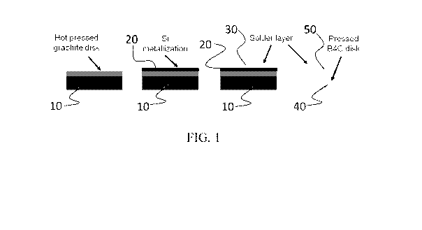
[0018] Figure 1 is a schematic depiction of fabrication of a graphite
finishing layer and boron
carbide base substrate.
[0019] Figure 2 is an image of graphite, silicon carbide, and boron carbide
with solder pellets
placed on the surface.
[0020] Figure 3 shows the image of Figure 2 after softening and spreading of
the solder pellets.
[0021] Figure 4 is a schematic depiction of joining a finishing layer assembly
and a base
substrate assembly to form a substrate.
[0022] Figure 5 is an image of substrates that include a graphite finishing
layer and non-oxide
ceramic base substrates.
[0023] Figure 6 is an image of a boron carbide substrate with a graphite
finishing layer on the
surface.
[0024] The embodiments set forth in the drawings are illustrative in nature
and not intended to
be limiting of the scope of the detailed description or claims. Whenever
possible, the same
reference numeral will be used throughout the drawings to refer to the same or
like feature.
DETAILED DESCRIPTION
[0025] The present disclosure is provided as an enabling teaching and can be
understood more
readily by reference to the following description, drawings, examples, and
claims. To this end,
those skilled in the relevant art will recognize and appreciate that many
changes can be made to
the various aspects of the embodiments described herein, while still obtaining
the beneficial
results. It will also be apparent that some of the desired benefits of the
present embodiments can
be obtained by selecting some of the features without utilizing other
features. Accordingly, those
who work in the art will recognize that many modifications and adaptations are
possible and can
even be desirable in certain circumstances and are a part of the present
disclosure. Therefore, it
is to be understood that this disclosure is not limited to the specific
compositions, articles,
devices, and methods disclosed unless otherwise specified. It is also to be
understood that the
terminology used herein is for the purpose of describing particular aspects
only and is not
intended to be limiting.
- 4 -
CA 03018211 2018-09-18
WO 2017/161084 PCT/US2017/022653
[0026] Disclosed are components (including materials, compounds, compositions,
and method
steps) that can be used for, in conjunction with, in preparation for, or as
embodiments of the
disclosed reflective optical elements and methods for making reflective
optical elements. It is
understood that when combinations or subsets, interactions of the components
are disclosed,
each component individually and each combination of two or more components is
also
contemplated and disclosed herein even if not explicitly stated. If, for
example, if a combination
of components A, B, and C is disclosed, then each of A, B, and C is
individually disclosed as is
each of the combinations A-B, B-C, A-C, and A-B-C. Similarly, if components D,
E, and F are
individually disclosed, then each combination D-E, E-F, D-F, and D-E-F is also
disclosed. This
concept applies to all aspects of this disclosure including, but not limited
to, components
corresponding to materials, compounds, compositions, and steps in methods.
[0027] In this specification and in the claims which follow, reference will be
made to a number
of terms which shall be defined to have the following meanings:
[0028] The term "about" references all terms in the range unless otherwise
stated. For
example, about 1, 2, or 3 is equivalent to about 1, about 2, or about 3, and
further comprises from
about 1-3, from about 1-2, and from about 2-3. Specific and preferred values
disclosed for
components, and like aspects, and ranges thereof, are for illustration only;
they do not exclude
other defined values or other values within defined ranges. The compositions
and methods of the
disclosure include those having any value or any combination of the values,
specific values,
more specific values, and preferred values described herein.
[0029] As used herein, contact refers to direct contact or indirect contact.
Elements in direct
contact touch each other. Elements in indirect contact do not touch each
other, but are otherwise
joined. Elements in contact may be rigidly or non-rigidly joined. Contacting
refers to placing
two elements in direct or indirect contact. Elements in direct (indirect)
contact may be said to
directly (indirectly) contact each other.
[0030] Ordering of layers in a sequence of layers in the present optical
elements will be
described relative to the substrate. Description of the ordering of the layers
herein is irrespective
of the orientation of the substrate. The substrate forms the base of the
optical element.
[0031] As used herein, the term "on" refers to direct or indirect contact. If
one layer is referred
to herein as being on another layer, the two layers are in direct or indirect
contact.
- 5 -
CA 03018211 2018-09-18
WO 2017/161084 PCT/US2017/022653
[0032] Unless otherwise specified herein, the terms "finish" or "surface
finish" refer to the
root-mean-square (rms) roughness of a surface. A surface with low roughness is
said to have a
low finish and a surface with high roughness is said to have a high finish.
Optical surfaces with
low finish are smoother and are preferable for the optical elements described
herein. As used
herein "low finish" refers to a surface having a root-mean-square (rms)
roughness as disclosed
herein.
[0033] Reference will now be made in detail to illustrative embodiments of the
present
description.
[0034] The present description provides a substrate for reflective optical
elements. The
substrate has light weight, high stiffness, and a surface with a low finish or
a surface capable of
being processed to a low finish. The present description also provides
reflective optical elements
utilizing the substrate. The reflective optical element may also include a
reflective layer or a
reflective stack on the surface of the substrate. A reflective stack is a
combination of two or
more layers that cooperate to provide reflection or other optical effect.
[0035] The substrate may include a base substrate and a finishing layer on the
base substrate.
The finishing layer is in direct or indirect contact with the base substrate.
As used herein, a
finishing layer is a layer having a surface that can be processed to a low
finish. A reflective layer
or reflective stack may be formed directly on the finishing layer. If the
finishing layer is absent,
the reflective layer or reflective stack may be formed directly on the base
substrate.
[0036] The substrate may include one or more intervening layers between the
finishing layer
and the base substrate. The one or more intervening layers may include a
metallization layer, an
adhesion layer, and/or a solder layer. The one or more intervening layers may
improve adhesion
between the finishing layer and the base substrate.
[0037] Selection of the base substrate is motivated by the design objectives
of light weight and
retention of figure in mechanically demanding applications. One important
property guiding
selection of the base substrate material is specific stiffness, which is
defined as the ratio (E/p) of
elastic modulus (E) to density (p). Other relevant material properties include
thermal expansion
(CTE), dimensional stability, environmental compatibility (corrosion,
radiation), finishing
capabilities (e.g. ability to diamond turn and/or polish to optical quality);
compatibility with
reflective coatings, and cost.
- 6 -
CA 03018211 2018-09-18
WO 2017/161084 PCT/US2017/022653
[0038] For extreme lightweight mirrors, beryllium (Be) is the de facto
standard. Be has the
highest specific stiffness of any metal (E = 4.25 x 10⁷ p
= 0.067 lbm/in3, E/p = 6.34 x 10⁸
lbf-in/lbm) and is suitable for space applications because its ability to
block cosmic radiation.
The finished cost of Be mirrors is very high, however, and Be cannot be
directly machined
(diamond turned) to a low finish. Low finish of Be substrates requires plating
of Be with a
finishing layer capable of being diamond machinable. Toxicity is a key
drawback of Be. Dust
or fumes from Be processing carry significant health risks (berylliosis).
Because of the
drawbacks associated with Be, Be mirrors are reserved for applications in
which the material
performance of Be far outweighs the cost (typically space applications).
[0039] The present description provides base substrates with performance
comparable to Be
that lack the drawbacks associated with Be. The only class of materials with
specific stiffness
comparable to Be is ceramics. Non-oxide ceramics, in particular, have high
specific stiffness. In
embodiments herein, the base substrate is a non-oxide ceramic. Preferred base
substrates in
accordance with the present description include carbides. Representative
carbides include boron
carbide and silicon carbide. Boron carbide has a specific stiffness of 7.47 x
108 lbf-in/lbm and
silicon carbide has a specific stiffness of 5.54 x 10⁸ lbf-in/lbm. Boron
carbide blocks cosmic
radiation and can be used in aerospace applications. Both materials can also
be hot pressed
and/or machined to near net shape.
[0040] Carbides have not been widely used as substrates for reflective optics
because they have
high hardness and are not amenable to diamond turning. As a result, it becomes
necessary to
apply a finishing layer to carbides to achieve substrates with low finish. In
applications requiring
high stability of figure in mechanically demanding deployment environments, it
has heretofore
been challenging to find a suitable material for the finishing layer.
[0041] This description provides a finishing layer for carbide base
substrates. The finishing
layer is graphite or a graphite-containing material. Graphite is a low density
material that
features chemical inertness, low coefficient of thermal expansion, and low
elastic modulus.
Graphite is also diamond turnable and when used as a thin finishing layer, has
little effect on
figure over wide temperature ranges.
[0042] The substrate may include a ceramic base substrate with a finishing
layer. In some
embodiments, the ceramic base substrate is a non-oxide ceramic and the
finishing layer is
graphite or a graphite-containing material. The base substrate may comprise or
consist
- 7 -
CA 03018211 2018-09-18
WO 2017/161084 PCT/US2017/022653
essentially of a non-oxide ceramic. The finishing layer may comprise or
consist essentially of
graphite. In some embodiments, the non-oxide ceramic is a carbide and the
substrate includes a
carbide base substrate and a finishing layer. In some embodiments, the
substrate includes a
carbide base substrate and graphite or a graphite-containing material as a
finishing layer. One
preferred embodiment includes a substrate with boron carbide as a base
substrate and graphite as
a finishing layer. Another preferred embodiment includes a substrate with
silicon carbide as a
base substrate and graphite as a finishing layer. Graphite may be in direct or
indirect contact
with the base substrate.
[0043] The specific stiffness of the ceramic base substrate may be at least
2.0 x 10⁸ lbf-in/lbm,
or at least 4.0 x 10⁸ lbf-in/lbm, or at least 6.0 x 10⁸ lbf-in/lbm, or at
least 7.0 x 10⁸ lbf-in/lbm, or in
the range from 2.0 x 10⁸ lbf-in/lbm to 1.0 x 10⁹ lbf-in/lbm, or in the range
from 3.0 x 10⁸ lbf-in/lbm
to 9.0 x 10⁸ lbf-in/lbm, or in the range from 4.0 x 10⁸ lb-in/lb m to 8.0 x
109 lbf-in/lbm, or in the
range from 4.5 x 10⁸ lbf-in/lbm to 7.5 x 10⁹ lbf-in/lbm.
[0044] Graphite may be deposited directly on the base substrate or formed
independent of the
base substrate and joined to the base substrate. Graphite may be formed by hot
isostatic pressing
of graphite powder, sputtering, or a vapor deposition technique. Graphite may
be machined,
diamond turned, or polished before or after joining to the base substrate. In
one embodiment,
graphite is formed independent of the base substrate and is processed to a
shape that conforms to
the shape of the surface of the base substrate. Graphite may also be obtained
from a commercial
source. Low porosity graphite is preferred.
[0045] To improve durability and/or adhesion, in certain embodiments, one or
more
intervening layers may be placed between graphite and the base substrate. The
one or more
intervening layers may include a metallization layer, an adhesion layer, a
metal carbide-forming
layer and/or a solder layer.
[0046] Metallization layers include Si. The metallization layer may be formed
on the graphite
finishing layer and/or the base substrate before joining the graphite
finishing layer and base
substrate. The surface to which the metallization layer is applied may be
roughened before
applying the metallization layer. Surface roughening may be achieved by
grinding (to form
random surface features or surface features such as grooves or ridges that are
aligned), bead
blasting, or with an elastomeric release sheet having embedded particles
arranged in a desired
pattern to create an engineered surface with controlled roughness. The
roughened surface may
- 8 -
CA 03018211 2018-09-18
WO 2017/161084 PCT/US2017/022653
improve adhesion of the metallization layer to the surface of a graphite
finishing layer and/or
surface of a carbide base substrate.
[0047] A metal carbide-forming layer may be formed on the surface of a
graphite finishing
layer and/or carbide base substrate before joining the graphite finishing
layer and carbide base
substrate. The metal carbide-forming layer may be a metal (e.g. Ti, Zr, Y, or
Cr) capable of
forming an interfacial metal carbide layer with graphite and/or the carbide
base substrate. The
metal carbide-forming layer may be between a graphite finishing layer and a
carbide base
substrate. In embodiments, a metal carbide-forming layer is in direct contact
with a graphite
finishing layer and a carbide base substrate is in direct contact with the
metal carbide-forming
layer. Separate metal carbide-forming layers may be formed on a graphite
finishing layer and a
carbide base substrate and separate metallization layers may be formed on the
metal carbide-
forming layers formed on each of a graphite finishing layer and a carbide base
substrate.
[0048] In embodiments, the interfacial metal carbide layer may improve
adhesion with an
overlying metallization layer. In embodiments, a metal carbide-forming layer
is formed between
a graphite finishing layer and a metallization layer. The metal-carbide
forming layer may be in
direct contact with the graphite finishing layer and the metallization layer
may be in direct
contact with the metal carbide-forming layer. In embodiments, a metal carbide-
forming layer is
formed between a carbide base substrate and a metallization layer. The metal-
carbide forming
layer may be in direct contact with the carbide base substrate and the
metallization layer may be
in direct contact with the metal carbide-forming layer.
[0049] The solder layer may contain Ti or a rare earth element. The
composition of the solder
may inhibit formation of oxide or nitride barrier layers at the surface of the
base substrate and/or
finishing layer. In some embodiments, the solder layer is applied directly to
either or both of a
graphite finishing layer and a carbide base substrate. In other embodiments, a
metallization layer
is present on a graphite finishing layer and/or carbide base substrate and a
solder is applied
directly to the metallization layer. The metallization layer may adhere
strongly to the graphite
finishing layer and/or carbide base substrate and the solder may be selected
to adhere strongly to
the metallization layer. The solder preferably has a low melting point (less
than 250 C, or less
than 225 C, or less than 200 C, or less than 175 C) to reduced temperature-
induced shape
distortions when joining the finishing layer and base substrate. Solder layers
include commercial
metal solders such as S-Bond 220 (a lead-free solder based on Sn-Ag-Ti alloys,
available from S-
- 9 -
CA 03018211 2018-09-18
WO 2017/161084 PCT/US2017/022653
Bond Technologies (Lansdale, PA)) or S-Bond 220M (a lead-free solder based on
Sn-Ag-Ti-Mg
alloys, available from S-Bond Technologies (Lansdale, PA)). Indium solders
optimized for
joining of non-metallic materials, such as solders #1E, #3, #4, #290 available
from Indium
Corporation (Utica, NY) may also be used. The thickness of the solder layer
may be less than
4.0 mil, or less than 3.0 mil, or less than 2.0 mil, or less than 1.0 mil, or
between 0.25 mil and 4.0
mil, or between 0.5 mil and 3.0 mil, or between 0.75 mil and 2.5 mil, or
between 1.0 mil and 2.0
mil.
[0050] Adhesion layers include metals (e.g. Ti, Zr, Yb, Cr, Pd). The adhesion
layer may be
applied as a separate layer or embedded in graphite. An adhesion layer may be
included between
a metallization layer and the graphite finishing layer or between a
metallization layer and a
carbide base substrate. In one embodiment, an Si metallization layer is formed
on a metal
adhesion layer and a solder layer is formed on the Si metallization layer. The
Si metallization
layer may improve wetting of the solder and the adhesion layer may improve
adhesion of the Si
metallization layer to a graphite finishing layer and/or base carbide
substrate.
[0051] The one or more intervening layers may also include an organic adhesive
layer. The
organic adhesive layer may be formed from an organic adhesive that is
thermally curable,
moisture curable, or radiation curable. Representative organic adhesives
include epoxies, epoxy
resins, phenol-formaldehyde resins, silicones, urethanes, urethane pre-
polymers, acrylates, and
methacrylates. The organic adhesive may also contain discrete particles of a
material with a low
coefficient of thermal expansion (e.g. glass) to increase stiffness and reduce
the overall
coefficient of thermal expansion of the organic adhesive. The thickness of the
organic adhesive
layer may be less than 2.0 mil, or less than 1.5 mil, or less than 1.0 mil, or
less than 0.5 mil, or
between 0.25 mil and 2.0 mil, or between 0.5 mil and 1.5 mil, or between 0.75
mil and 1.25 mil.
[0052] In one embodiment, the reflective optical element includes a graphite
finishing layer in
direct contact with a carbide base substrate. In a second embodiment, the
reflective optical
element includes a graphite finishing layer in direct contact with a
metallization layer and a
metallization layer in direct contact with a carbide base substrate. In a
third embodiment, the
reflective optical element includes a graphite finishing layer in direct
contact with a solder layer
and a solder layer in direct contact with a carbide base substrate. In a
fourth embodiment, the
reflective optical element includes a graphite finishing layer in direct
contact with an organic
adhesive layer and an organic adhesive layer in direct contact with a carbide
base substrate. In a
- 10 -
CA 03018211 2018-09-18
WO 2017/161084 PCT/US2017/022653
fifth embodiment, the reflective optical element includes a graphite finishing
layer in direct
contact with a metallization layer, a metallization layer in direct contact
with a solder layer, and a
solder layer in direct contact with a carbide base substrate. In a sixth
embodiment, the reflective
optical element includes a graphite finishing layer in direct contact with a
first metallization
layer, a first metallization layer in direct contact with a solder layer, a
solder layer in direct
contact with a second metallization layer, and a second metallization layer in
direct contact with
a carbide base substrate.
[0053] Figure 1 illustrates initial steps in an embodiment for fabricating a
substrate in
accordance with the present description. In this example, a graphite finishing
layer was formed
independent of a boron carbide base substrate and the graphite finishing layer
and boron carbide
base substrate are joined. The graphite finishing layer 10 is formed by a hot
pressing technique
and configured as a disk. A typical diameter for a graphite disk is 2 inches.
One surface of
graphite finishing layer 10 was polished. If desired, the graphite surface may
be processed to a
particular shape (e.g. flat, curved, spherical, aspherical). A silicon
metallization layer 20 was
formed by sputtering on the polished surface graphite finishing layer 10. The
thickness of silicon
metallization layer 20 was between 25 i_tm and 50 1_1111. A solder layer 30
was formed on silicon
metallization layer 20. To form the solder layer, the graphite finishing layer
10 with silicon
metallization layer 20 was heated and a pellet of solder was deposited on the
surface. After the
pellet softened, a scraper tool was used to distribute the solder uniformly
across the surface of
silicon metallization layer 20. The scraper tool may also remove surface
oxides that may form
on the Si metallization layer to expose underlying unoxidized Si, which is
expected to provide
better solder wetting than oxidized forms of Si. S-Bond 5B220M solder was used
in the
example of Fig. 1.
[0054] A carbide base substrate 40 was prepared separately. Carbide base
substrate 40 was a
boron carbide base substrate made through powder pressing and firing under an
inert gas
atmosphere (e.g. Ar) at 2100 C ¨ 2200 C. Carbide base substrate 40 was
configured as a disk.
The approximate chemical formula of carbide base substrate 40 was B4C. One
surface of carbide
base substrate 40 was polished. If desired, a surface of the carbide base
substrate may be
processed to complement the shape of a shaped surface of graphite finishing
layer 10. If, for
example, graphite finishing layer 10 has a surface with a convex shape, a
surface of carbide base
substrate 40 may have a concave shape to facilitate joining of graphite
finishing layer 10 with
- 11 -
CA 03018211 2018-09-18
WO 2017/161084 PCT/US2017/022653
carbide base substrate 40. Solder layer 50 was formed directly on the surface
of carbide base
substrate 40. To form solder layer 50, carbide base substrate 40 was heated, a
pellet of solder
was placed on the surface, and upon softening, the solder was scraped to
provide a uniform layer.
S-Bond 5B220M solder was used for solder layer 50.
[0055] Fig. 2 shows images of samples of graphite finishing layers (pie-shaped
samples in top
row), silicon carbide base substrates (two truncated circular samples in
second row) and boron
carbide base substrates (bottom two rows) with solder pellets before
softening. The samples of
graphite finishing layer included a silicon metallization layer and a solder
pellet was placed
directly on the silicon metallization layer. The samples of silicon carbide
base substrates and
boron carbide base substrates lacked a silicon metallization layer and the
solder pellets were
placed directly the surface. Fig. 3 shows images of the same samples after
softening of the
solder. As noted hereinabove, the softened solder was scraped across the
surface to provide a
more uniform solder layer.
[0056] Figure 4 shows joining of a finishing layer assembly to a base
substrate assembly to
form a substrate. The base substrate assembly includes the boron carbide base
substrate shown
in Figure 1 and the finishing layer assembly includes the graphite finishing
layer shown in Figure
1. Finishing layer assembly 60 includes graphite finishing layer 10, silicon
metallization layer
20, and solder layer 30. Base substrate assembly 70 includes boron carbide
base substrate 40 and
solder layer 50. Finishing layer assembly 60 and base substrate assembly 70
are oriented so that
solder layer 30 faces solder layer 50 (shown at A in Fig. 4). Finishing layer
assembly 60 and
base substrate assembly 70 are then joined by applying mechanical force to
press them together
to form substrate 80 (shown at B in Fig. 4). A lateral shearing force may also
be applied.
Joining is performed while solder layer 30 and solder layer 50 are molten. The
mechanical force
thins solder layer 30 and solder layer 50, provides a uniform solder layer,
and eliminates gaps or
air bubbles within solder layer 30, solder layer 50 or the interface between
solder layer 30 and
solder layer 50. Excess solder that extrudes away from the interface is
removed. Thinning of the
solder layer is desirable because most solders have high coefficients of
thermal expansion and
thus deform when exposed to high temperature environments. Deformation of the
solder may
cause repositioning or misalignment of substrate 80 during deployment.
[0057] Figure 5 shows representative substrates made by joining various
samples depicted in
Fig. 3. The upper pie-shape sample is a graphite finishing layer with a
silicon metallization layer
- 12 -
CA 03018211 2018-09-18
WO 2017/161084 PCT/US2017/022653
on its joined surface. The larger lower samples are non-oxide ceramic base
substrates. Silicon
carbide (SiC) and boron carbide (B4C) base substrates are shown as listed in
Fig. 5. The light-
colored layer on the surface of the base substrates is a solder layer. Two
different solders were
used (S-Bond 220 and S-Bond 220M). Solder at the interface between the
graphite finishing
layer and the non-oxide ceramic base substrate joins the pieces together to
form substrates.
[0058] After joining, substrate 80 is cooled and then thinned by removing a
portion of graphite
finishing layer 10 to form substrate 85 (shown at C in Fig. 4). Removal of
graphite finishing
layer 10 can be accomplished by sawing, grinding, polishing, or otherwise
abrading or depleting
material from the surface of graphite finishing layer 10. Boron carbide base
substrate 40 may
also be thinned to further reduce the weight of substrate 85. After thinning,
the graphite surface
of substrate 80 may be further processed by polishing or diamond turning to a
low finish (shown
at D in Fig. 4). A reflecting layer or reflecting stack may subsequently be
formed on the graphite
surface of substrate 80.
[0059] Figure 6 depicts a sample having a graphite layer on a boron carbide
substrate and an
image of the surface of the graphite layer. The image indicates that the peak-
to-valley roughness
of the surface of the graphite layer is 285 A and that the finish (rms
roughness) of the graphite
layer is 4.6 A.
[0060] In different embodiments, the finish (rms roughness) of a surface of a
graphite or
graphite-containing finishing layer is less than 500 A, or less than 300 A, or
less than 200 A, or
less than 100 A, or less than 50 A, or less than 25 A, or less than 10 A, or
in the range from 5 A
to 500 A, or in the range from 10 A to 400 A, or in the range from 25 A to 500
A, or in the range
from 50 A to 300 A, or in the range from 50 A to 200 A, or in the range from
50 A to 150 A, or
in the range from 50 A to 100 A, or in the range from 100 A to 500 A, or in
the range from 100
A to 300 A. In different embodiments, the peak-to-valley (PV) roughness of a
surface of a
graphite or graphite-containing finishing layer is less than 1500 nm, or less
than 1250 nm, or less
than 1000 nm, or less than 750 nm, or less than 500 nm, or less than 400 nm,
or less than 300
nm.
[0061] In certain embodiments, a supplemental finishing layer is formed on the
graphite
surface of a substrate. Representative supplemental finishing layers for a
graphite surface
include metals, oxides, DLC (diamond-like carbon), B and Si. Metals include
Ni, Cu, W, Ti, Zr,
Hf, Nb, Ta, Mo, and Au. Oxides include A1203 and 5i02. Zr, Hf, Nb, Ta, Mo,
A1203, and 5i02
- 13 -
CA 03018211 2018-09-18
WO 2017/161084 PCT/US2017/022653
have coefficients of thermal expansion that are similar to the coefficient of
thermal expansion of
graphite and may be advantageous when the intended application of the optical
element includes
exposure to temperatures that vary over a wide range. The supplemental
finishing layer on the
graphite surface may also be a reflective layer. The supplemental finishing
layer on the graphite
surface may be polished or diamond turned to a low finish. The supplemental
finishing layer on
the graphite surface may be selected so as to permit attainment of a lower
finish than would be
possible from a graphite surface alone.
[0062] The finish (rms roughness) of a surface of the supplemental finishing
layer may be less
than 300 A, or less than 200 A, or less than 100 A, or less than 50 A, or less
than 30 A, or in the
range from 25 A to 300 A, or in the range from 25 A to 250 A, or in the range
from 25 A to 200
A, or in the range from 25 A to 150 A, or in the range from 25 A to 100 A, or
in the range from
40 A to 200 A, or in the range from 40 A to 125 A. The peak-to-valley (PV)
roughness of a
surface of the supplemental finishing layer may be less than 1000 nm, or less
than 80 nm, or less
than 600 nm, or less than 400 nm, or less than 300 nm.
[0063] The substrate disclosed herein may function as a substrate for an
optical element that
include a variety of reflective layers or reflective stacks formed on a
finished graphite surface or
on a supplemental finishing layer formed on a graphite finishing layer. The
reflective coating
preferably provides high reflectivity in one or more of the visible (VIS),
near infrared (NIR),
shortwave infrared (SWIR), midwave infrared (MWIR), and long wave infrared
(LWIR) bands.
The reflective coating may be a layer of a single material or a multilayer
stack of two or more
materials. In one embodiment, the reflective coating includes a reflective
layer and one or more
tuning layers. The reflective coating may optionally include a barrier layer,
one or more
interface layers, and one or more protective layers. When present, the one or
more protective
layers overlie the other layers in the stack.
[0064] The reflective layer may include a metal layer or a transition metal
layer. The reflective
layer preferably has high reflectivity at wavelengths in the VIS, NIR, SWIR,
MWIR, and LWIR
spectral bands. The reflective metal may be metallic, non-ionic, a pure metal
or metal alloy,
and/or zero valent. The reflective layer may include one or more elements
selected from the
group consisting of Ag, Au, Al, Rh, Cu, Pt and Ni. The thickness of the
reflective transition
metal layer may be in the range from 75 nm to 350 nm, or in the range from 80
nm to 150 nm, or
in the range from 90 nm to 120 nm.
- 14 -
CA 03018211 2018-09-18
WO 2017/161084 PCT/US2017/022653
[0065] The reflective coating may include one or more tuning layers. The one
or more tuning
layers are positioned between the protective layer(s) of the reflective
coating and the graphite or
supplemental finishing layer. In one embodiment, the tuning layer(s) are
positioned between the
reflective layer and the protective layer(s) of the reflective coating. Tuning
layer(s) are designed
to optimize reflection in defined wavelength regions. Tuning layer(s)
typically include an
alternating combination of high and low refractive index materials, or high,
intermediate, and
low refractive index materials. Materials used for tuning layers are
preferably low absorbing in
the wavelength range of from 0.41.tm to 15.0 jim. Representative materials for
tuning layers
include YbF3, GdF3, YF3, YbOxFy, GdF3, Nb2O5, Bi203, and ZnS. The tuning
layer(s) may have
a thickness in the range of 75 nm to 300 nm. In one embodiment, the reflective
coating includes
YbF3 and ZnS as tuning layers.
[0066] The reflective layer and tuning layer(s) may be in direct contact or
one or more interface
layers may be present between the reflective layer and tuning layer(s). The
interface layer(s)
may promote adhesion or provide galvanic compatibility between the reflective
layer and tuning
layer(s). The interface layer(s) needs to have a thickness sufficient for
adhesion, but must also
be thin enough to minimize absorption of light reflected from the reflective
layer. The interface
layer(s) positioned between the reflective layer and the tuning layer(s) may
have a thickness in
the range of 5 nm to 20 nm, or 8 nm to 15 nm, or 8 nm to 12 nm. The interface
layer(s)
positioned between the reflective layer and the tuning layer(s) may include
one or more of
Nb2O5, TiO2, Ta205, Bi203, ZnS and A1203.
[0067] In one embodiment, the reflective layer is in direct contact with the
graphite or
supplemental finishing layer. In another embodiment, the optical element
includes a barrier
layer and/or an interface layer between the reflective layer and the graphite
or supplemental
finishing layer. In still another embodiment, the optical element includes a
barrier layer in direct
contact with the graphite or supplemental finishing layer. In yet another
embodiment, the optical
element includes a barrier layer in direct contact with the graphite or
supplemental finishing
layer and an interface layer in direct contact with the barrier layer. The
interface layer may
promote adhesion between the reflective layer and barrier layer, or between
the reflective layer
and the galvanic-compatibility layer. The interface layer may also insure
galvanic compatibility
of the reflective coating with the graphite or supplemental finishing layer,
or galvanic
- 15 -
CA 03018211 2018-09-18
WO 2017/161084 PCT/US2017/022653
compatibility of the barrier layer with the reflective layer. The barrier
layer may insure galvanic
compatibility between the reflective layer and the graphite substrate.
[0068] Representative barrier layers include Si3N4, SiO2, TiAlN, TiAlSiN,
TiO2, DLC
(diamond-like carbon), Al, CrN, and SixNyOz. The barrier layer may have a
thickness in the
range from 100 nm to 50 m, or in the range from 500 nm to 10 m, or in the
range from 1 p.m
to 5 m. One criterion for determining the thickness of the barrier is the
number of hours the
article will have to withstand the salt fog test. The longer the duration of
the salt fog test, the
greater the required thickness of the barrier layer. For a salt fog test of 24
hours, a barrier layer
of 10 m may be sufficient. The thickness of the barrier layer can also be
adjusted to
accommodate changes in temperature without distorting the figure of the
optical element.
Thermal stresses increase as the operational temperature range increases, so
thinner barrier layers
are recommended to avoid figure distortion in deployment environments
experiencing large
swings in temperature.
[0069] Representative interface layers positioned between the graphite or
supplemental
finishing layer and the reflective layer include one or more of Ni, Cr, Ni-Cr
alloys (e.g.
Nichrome), Ni-Cu alloys (e.g. Monel), Ti, TiO2, ZnS, Pt, Ta205, Nb2O5, A1203,
AIN, A10xNy, Bi,
Bi203. Si3N4, SiO2, SiOxNy, DLC (diamond-like carbon), MgF2, YbF3, and YF3.
The interface
layer may have a thickness in the range from 0.2 nm to 25 nm, where the lower
end of the
thickness range (e.g. 0.2 nm to 2.5 nm, or 0.2 nm to 5 nm) is appropriate when
the interface layer
is a metal (to prevent parasitic absorbance of light passing through the
reflective coating) and the
higher end of the thickness range (e.g. 2.5 nm to 25 nm, or 5 nm to 25 nm) is
appropriate when
the interface layer is a dielectric.
[0070] The protective layer provides resistance to scratches, resistance to
mechanical damage,
and chemical durability. Representative materials for the protective layer
include YbF3, YbFx0y,
YF3 and Si3N4. The protective layer(s) is the top layer of the reflective
coating. The protective
layer(s) may have a thickness in the range of 60 nm to 200 nm.
[0071] Unless otherwise expressly stated, it is in no way intended that any
method set forth
herein be construed as requiring that its steps be performed in a specific
order. Accordingly,
where a method claim does not actually recite an order to be followed by its
steps or it is not
otherwise specifically stated in the claims or descriptions that the steps are
to be limited to a
specific order, it is no way intended that any particular order be inferred.
- 16 -
CA 03018211 2018-09-18
WO 2017/161084 PCT/US2017/022653
[0072] It will be apparent to those skilled in the art that various
modifications and variations
can be made without departing from the spirit or scope of the illustrated
embodiments. Since
modifications, combinations, sub-combinations and variations of the disclosed
embodiments that
incorporate the spirit and substance of the illustrated embodiments may occur
to persons skilled
in the art, the description should be construed to include everything within
the scope of the
appended claims and their equivalents.
- 17 -