Note : Les descriptions sont présentées dans la langue officielle dans laquelle elles ont été soumises.
CA 03018888 2018-09-24
WO 2017/184455 PCT/US2017/027674
SEMICONDUCTOR LENS OPTIMIZATION OF FABRICATION
CROSS-REFERENCE TO RELATED APPLICATIONS
[0001] This application claims the benefit of U.S. Patent Application No.
15/133,094,
filed April 19, 2016.
BRIEF DESCRIPTION OF THE INVENTION
[0002] Embodiments comprise a system created through fabricating a lens array
through which lasers are emitted. The lens array may be fabricated in the
semiconductor
substrate used for fabricating the lasers or may be a separate substrate of
other transparent
material that would be aligned to the lasers. In some embodiments, more lenses
may be produced
than will eventually be used by the lasers. The inner portion of the substrate
may be etched with
the lenses that will be used for emitting lasers, and the outer portion of the
substrate may be
etched with lenses that will not be used for emitting lasers ¨ rather, through
etching these
additional lenses, the inner lenses may be created with a higher quality.
BACKGROUND
[0003] Lenses ¨ optical devices that transmit and refract light ¨ or arrays of
lenses, may
be fabricated on the back of a semiconductor laser substrate for back emitting
VCSEL (Vertical
Cavity Surface Emitting Lasers) or VECSELs VCSEL (Vertical (Extended or
External) Cavity
Surface Emitting Lasers) designs. A VCSEL is a type of semiconductor laser
diode with laser
beam emission perpendicular from the top surface. In contrast, conventional
edge-emitting
semiconductor lasers emit from surfaces formed by cleaving the individual chip
out of a wafer.
VECSELs then are a type of VCSELs that have been reconfigured to have the
cavity extended
outside of the wafer. In an alternative approach, the lens array may be
fabricated separately, in a
different material, such as glass or transparent polymer. The lens array may
be configured to
align, by mechanical means, to the lasers in an assembly or manufacturing
process. Such
fabrication of the lens arrays may generally be performed by transferring a
pattern from
photoresist into the surface of the substrate by etching. An etched lens may
be characterized by
its respective curvature or Radius of Curvature (ROC), and this curvature may
be a significant
aspect of the performance of the lens. An etched lens may also be a Fresnel or
diffractive
structure where the light is controlled by a pattern that produces a similar
phase delay of the light
as a conventional lens. In that case, a pattern from photoresist (or an
electron beam resist, or a
610633921.1
- 1 -
CA 03018888 2018-09-24
WO 2017/184455 PCT/US2017/027674
resist patterned by physical imprinting, or stamping) may also be transferred
into the surface of
the substrate material by etching.
BRIEF DESCRIPTION OF THE DRAWINGS
[0004] FIG. 1 illustrates an example embodiment of an etched array of lenses
where
functional lenses are aligned to the lasers;
[0005] FIG. 2 illustrates an example embodiment of an etched array of lenses
where
functional lenses are purposely misaligned (offset) in relation to the lasers;
[0006] FIG. 3 illustrates an example embodiment of an etched array of lenses
where
functional lenses, shown in detail, are surrounded by exterior, non-function
lenses; and
[0007] FIG. 4 illustrates an example embodiment of a method for transferring a
pattern
from photoresist into a substrate by etching.
DETAILED DESCRIPTION OF ILLUSTRATIVE EMBODIMENTS
[0008] Etching generally may be the process of using chemicals to fabricate a
substrate
to remove one or more layers, with parts of the substrate being unexposed to a
particular etching
iteration when being covered by a masking material that resists etching. The
lens fabrication
process requires the gradual etching away or erosion of a photoresist so that
the shape of the
photoresist structure is transferred into the substrate. The rate of this lens
fabrication process
does not consume the chemical reactive species in the etch process as fast as
the slower etching
process of the photoresist material. Thus, the ratio of the etching of the
substrate material to the
photoresist material ideally should be constant throughout the etching
process. A problem with
etching an array of lenses into a substrate is that doing so may cause a
loading effect that
produces different etch rates at different locations due to the ratio of areas
of the etch material to
the areas of the more slowly etched material or photoresist. This is because,
if more area of the
substrate is uncovered by photoresist for etching, the rate will slow down due
to the lower
availability of the chemical reactive species that is used for etching in that
localized region. The
availability of the chemical reactive species may be adjusted with complex gas
flows and
composition experiments, with electrical bias adjustments, or with a
combination of these two
techniques. However, the results of etching are, by nature, complex, and to de-
convolve so many
variables is a difficult problem to solve.
- 2 -
CA 03018888 2018-09-24
WO 2017/184455 PCT/US2017/027674
[0009] A solution to this problem may comprise producing more than enough
lenses so
that the lenses that are functional (i.e., light is directed through the lens)
are conveniently
positioned on the interior portion in an array and have the same ratio of the
area of uncovered
substrate material to the area of photoresist material across the array. This
same ratio of the area
of exposed substrate material to the area of non-etched photoresist material
may be accomplished
through these non-functional exterior lenses (i.e., light is not directed
through the lenses),
because these exterior lenses comprise etched material just like the
functional lenses. Therefore,
each functional lens may be surrounded by the same number of adjoining lenses
(and these
adjoining lenses may be other functional lenses or a combination of functional
lenses and non-
functional lenses). The distance between the center of any functional lens and
the center of any
adjacent lens (whether it be functional or non-functional lenses) may be the
same. Likewise, the
distance from the center of any lens and any adjacent lens may be the same,
such that the
distance between any two adjacent lens are the same, regardless of whether one
lens is functional
and the other is not, both lenses are functional or both lenses are non-
functional. These interior
lenses may be used for characterization of etch parameters, while the exterior
lenses in the array
may have a different ratio of etched area to non-etched or patterned areas.
[0010] In some embodiments, the solution described above may be performed by a
system. The system itself may generally include a processor and one or more
memories
containing a program including instructions, which, when executed on the
processor are
configured to perform an operation for manufacturing lenses. For example, a
computer system
may be used to design the layout of the lenses and to direct the equipment
manufacturing the
lenses.
[0011] These lens arrays may be fabricated in a variety of processes to
produce exterior
and interior lenses, such as through wet etching, anisotropic wet etching, and
plasma etching. A
greyscale lithography process may also be used to produce the interior and
exterior lenses.
Interior functional lenses may be several lens periods back from a border of
the substrate. The
non-functional exterior lenses may be non-functional save for having a
positional function in
producing uniform interior lenses.
[0012] In some embodiments, a thick material may also be deposited on the
substrate to
serve as a protective height barrier so that the lenses do not get scratched
if the substrate lands on
its lens side.
[0013] FIG. 1 illustrates an example embodiment of an etched array of lenses
100
where functional lenses 102 extend to the edge of the substrate. Lens array
100 contains only
- 3 -
CA 03018888 2018-09-24
WO 2017/184455 PCT/US2017/027674
functional lenses 102 (as opposed to non-functional lenses). These lenses may
be considered to
be functional as they are designed for the transmission of laser radiation. It
may be observed that
all the depicted lenses 102 are functional because each functional lens has a
corresponding laser
104 that is on the opposite side of the substrate and aligned (or purposefully
misaligned; see FIG.
2) to the lens. In this array, the lens 102a in the middle of the array 100
may be configured to
align to the VCSEL, while the next ring of lenses 102b may be purposefully
designed to have a
smaller pitch than the lens 102a, which produces beams that uniformly diverge.
In some
embodiments, there may also be a deposited material 106 built or constructed
on top of and
around lens array 100 to prevent scratches on the lenses.
[0014] It may be appreciated that, in some embodiments, the etching process
may cause
lens 102a to have a different Radius of Curvature (ROC) or of varying
dimension than the ROC
of lenses 102b. This is because the ratio of uncovered substrate material to
the more slowly
etched photoresist material surrounding lens 102a and lenses 102b may differ.
Lens 102a itself
comprises photoresist material, and is surrounded by lenses 102b, which also
comprise
photoresist material. The material between and surrounding the lenses is
unmasked substrate
surface which may be etched aggressively from the start of the process. In
contrast, lenses 102b
comprise photoresist material, but may not be completely surrounded by other
photoresist
material. Where a lens in lenses 102b is adjoined by other lenses in lenses
102b or by lens 102a,
that neighboring material is also slowly etched photoresist material. However,
toward the outer
edge of the substrate, lens 102b may not contain photoresist material. So, the
loading effect may
be different between lenses 102b and lens 102a. This means that the ratio of
area of uncovered
substrate material to area covered with photoresist differs between lenses in
lenses 102b (where
they are not surrounded by lenses comprising photoresist material) and lens
102a (which is
surrounded by other lenses comprising photoresist material). In other words,
since this ratio of
uncovered substrate area to the area covered by photoresist lens patterns
differs between lenses
in 102b and in 102a, the lenses of 102b may have a different ROC than the ROC
in lens 102a.
[0015] FIG. 2 illustrates another example embodiment of an etched array of
lenses 200
where functional lenses 202 extend to the edge of the substrate. However,
distinct from FIG. 1
where the depicted lenses 102 are functional because each depicted functional
lens 102 is aligned
with its corresponding laser 104, FIG. 2 illustrates, that all functional
lenses 202b, excluding lens
202a, may be purposefully misaligned (offset) from each of their corresponding
lasers 204. By
positioning or locating the lenses 202b in an offset from each of their
corresponding lasers 204,
- 4 -
CA 03018888 2018-09-24
WO 2017/184455 PCT/US2017/027674
the beams emitting from the lasers may be conveniently directed to a desired
convergence,
divergence and/or to a specific direction.
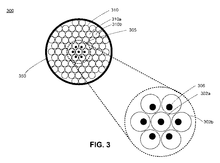
[0016] FIG. 3 illustrates an example embodiment of an etched array of lenses
300
where functional lenses 305, the lenses fully inside the dashed line, are
surrounded by exterior,
non-functional lenses 310, the lenses under and outside of the dashed line.
The functional lenses
are further broken out in detail. In fabricating lenses in such a manner, as
opposed to lens array
200 of FIG. 2, loading effects may be diminished, and more uniform lenses may
also be created.
While lens array 300 is depicted here as being substantially circular, it may
be appreciated that
there are embodiments that create a lens array in different shapes. FIG. 3
differs from FIG. 2 in
that, in FIG. 3, there is a ring of exterior, non-functional lenses 310 that
are etched into the
substrate. So, here, lens array 300 contains both functional lenses 305, and
non-functional lenses
310. The functional lenses 305 may be considered to be functional because each
functional lens
305 has a corresponding laser 306 that is on the opposite side of the
substrate and aligned (or
purposefully misaligned) to the lens. In this array of lenses 300, the lens
302a in the middle of
the array 300 is aligned to the VCSEL, while the next ring of lenses 302b may
be purposefully
designed to have a smaller pitch than the lens 302a, which produces beams that
uniformly
diverge, or a different alignment between the laser for lens 302a and the
lasers for lenses 302b.
Then, there are exterior, non-functional lenses 310 that are etched on the
substrate to reduce
loading effects on the functional lenses 305. There may also be a deposited
material 350 built on
top of and around lens array 300 to prevent scratches on the lenses.
[0017] Furthermore, as illustrated in FIG. 3, the distance between the center
of each
functional lens 305 and the center of the surrounding adjoining lenses
(whether it be a functional
lens 305 or non-functional lens 310) may be the same distance between the
centers of any two
adjacent lenses. For instance, the distance between the center of functional
lens 302a and the
center of adjacent functional lens 302b may be the same distance between the
center of non-
functional lens 310a and the center of adjacent non-functional lens 310b. Put
another way, the
distance from the center of any lens (functional or non-functional) to the
center of an adjacent
lens (functional or non-functional) is all the same.
[0018] In contrast to lens array 100 of FIG. 1 and lens array 200 of FIG. 2,
where
lenses 102b, 202b, 102a, and lens 202a experience different loading effects,
here, all functional
lenses 305 experience substantially similar loading effects, so all functional
lenses 305 have
substantially similar ROCs. These substantially similar loading effects are
due, in part, to the
presence of non-functional lenses 310, which surround the array of functional
lenses 305. In
- 5 -
CA 03018888 2018-09-24
WO 2017/184455 PCT/US2017/027674
contrast to the lenses of FIGS. 1 and 2, here, each functional lens is
surrounded by the same
number of other (functional or non-functional) lenses, so each functional lens
experiences the
same ratio of etched material to non-etched material. Since each functional
lens of functional
lenses 310 has the same ratio of rapidly etched material to slowly etched
material around it, it
experiences the same loading effects as the other functional lenses, so all
functional lenses 305
are produced with substantially the same ROC.
[0019] This design of an array of lenses 300 or other optical surfaces may
overcome
etch limitations in order to allow interior lenses 305 in lens array 300 to be
of higher uniformity
for better functional performance when compared to exterior lenses 310 in lens
array 300, which
are non-functional save for having a positional function for producing uniform
interior lenses
305. Additionally, this array of optical surfaces in lens array 300 may
overcome etch limitations
in order to allow interior lenses 305 in lens array 300 to be of higher
uniformity for better
functional performance as opposed to exterior (non-functional) lenses 310 in
lens array 300, and
other non-functional arrays of lenses that buffer functional lenses 305 from
exterior lenses 310.
[0020] Additionally as noted above and as shown in FIG. 3, the functional
lenses 305
within the lens array 300, excluding lens 302a, may be offset from their
respective laser 306
alignments to direct beams in a specified direction. Combinations of
misaligned beams and
aligned beams may be functional and have a non-functional lens etched to
reduce loading effects
on functional lenses 305.
[0021] A thick deposition of material may be deposited around the
circumference or
over the lenses 305 (not depicted in FIG. 3, but depicted in FIGS. 1 and 2)
and/or 310 (material
350), or a combination of each, so that a protective height is built up in
order not to scratch lens
305 or 310.
[0022] FIG. 4 illustrates an example embodiment of a method of transferring a
pattern
from photoresist 405 into a substrate 410 by etching. The flow or process 400
in FIG. 4 depicts a
photoresist structure 405 that may be melted onto the substrate 410. Once
melted on the substrate
410 or utilizing a different technique known to those skilled in the art of
transferring a
photoresist onto the substrate 410, a rounded shape is formed on the substrate
410. This rounded
shape on the substrate 410 may be exposed to an etch process. With an exposed
rounded shape,
the etching process may etch more rapidly and with a vertical directionality.
The etching process
may also be sensitive to many factors, including the amount of exposed
substrate material around
the photoresist. At the conclusion of the etching process, a certain shape may
be fully transferred
into the substrate 410. FIG. 4 illustrates an example embodiment of a single
photoresist
- 6 -
CA 03018888 2018-09-24
WO 2017/184455 PCT/US2017/027674
transferred onto the substrate 410; however, multiple or more than one
photoresists may be
transferred onto the substrate 410 at the same time.
[0023] Another embodiment includes fabrication of the lens shape directly into
the
photoresist by a process such as greyscale lithography. Those shapes may then
be used as lenses.
Alternatively, the pattern of shapes may also be etched into the substrate
material.
[0024] In an embodiment, a method for manufacturing lenses comprises etching a
layer
of photoresist over a substrate to form a lens array with a plurality of
lenses, wherein the lens
array further comprises an inner portion with a first set of lenses and an
outer portion with a
second set of lenses, wherein the second set of lenses is positioned adjacent
to and surrounds the
first set of lenses, wherein each lens in the first set of lenses is
surrounded by a same number of
lenses of either the first set of lenses or the second set of lenses, and
positioning each laser
among a plurality of lasers to correspond with each lens in the first set of
lenses and positioning
no laser to correspond with any of the lenses in the second set of lenses. In
the embodiment,
wherein etching the layer of photoresist is accomplished by at least one of: a
wet etching process,
an anisotropic wet etching process, a plasma etching process, and a dry
etching process. In the
embodiment, wherein etching a layer includes transferring a pattern for the
lens array from
photoresist into the substrate. In the embodiment, wherein the lens array is
circular in
configuration. In the embodiment, wherein the plurality of lasers are
positioned on the opposite
side of the substrate from the lens array and wherein each laser is configured
to emit light into
each lens in the first set of lenses. In the embodiment, wherein a first laser
is aligned to the center
of a first lens from the first set of lenses and a second laser is aligned to
be off-center of a second
lens from the first set of lenses. In the embodiment, wherein the substrate is
deposited with a
thick material to serve as a protective height barrier and prevent scratches.
In the embodiment,
wherein each lens of the first set of lenses comprises a substantially similar
Radius of Curvatures
(ROCs) and wherein each lens of the first set of lenses is configured to be a
length of several
lenses from a border of the substrate. In the embodiment, wherein a distance
from a center of any
lens among the first set of lenses or the second set of lenses and the center
of any adjacent lens is
the same. In the embodiment, wherein a first lens in the second set of lenses
comprises a smaller
pitch than a second lens in the second set of lenses.
[0025] In an embodiment, a system for manufacturing lenses comprises a
processor;
and one or memories in communication with the processor when the system is in
operation, the
one or more memories having stored thereon instructions that upon execution by
the processor at
least cause the system to form a lens array with a plurality of lenses,
wherein the lens array
- 7 -
CA 03018888 2018-09-24
WO 2017/184455 PCT/US2017/027674
further comprises an inner portion with a first set of lenses and an outer
portion with a second set
of lenses, wherein the second set of lenses is positioned adjacent and
surrounds the first set of
lenses, wherein each lens in the first set of lenses is surrounded by a same
number of lenses of
either the first set of lenses or the second set of lenses, and position each
laser among a plurality
of lasers to correspond with each lens in the first set of lenses and position
no laser to correspond
with any of the lenses in the second set of lenses. In the embodiment, wherein
the instructions
that cause the system to form a lens array cause the system to etch a layer of
photoresist over a
substrate to form the lens array, wherein the etch is accomplished by at least
one of: a wet
etching process, an anisotropic wet etching process, a plasma etching process,
and a dry etching
process. In the embodiment, wherein the instructions that cause the system to
etch the layer to
form the lens array cause the system to transfer a pattern from photoresist
into the substrate. In
the embodiment, wherein the lens array is circular in configuration. In the
embodiment, wherein
the plurality of lasers are positioned on the opposite side of the substrate
from the lens array and
wherein each laser is configured to emit light into each lens in the first set
of lenses. In the
embodiment, wherein a first laser is aligned to the center of a first lens
from the first set of lenses
and a second laser is aligned to be off-center of a second lens from the first
set of lenses. In the
embodiment, wherein the substrate is deposited with a thick material to serve
as a protective
height barrier and prevent scratches. In the embodiment, wherein each lens of
the first set of
lenses comprises a substantially similar Radius of Curvatures (ROCs) and
wherein each lens of
the first set of lenses is configured to be a length of several lenses from a
border of the substrate.
In the embodiment, wherein a distance from a center of any lens among the
first set of lenses or
the second set of lenses and the center of any adjacent lens is the same. In
the embodiment,
wherein a first lens in the second set of lenses comprises a smaller pitch
than a second lens in the
second set of lenses. In the embodiment, wherein the instruction that cause
the system to form
the lens array control a greyscale photolithography process. In the
embodiment, wherein the
instructions that cause the system to form the lens array cause the system to
transfer a pattern of
lens shapes to the substrate.
[0026] In an embodiment, a method for manufacturing lenses comprises forming a
lens
array with a plurality of lenses, wherein the lens array further comprises an
inner portion with a
first set of lenses and an outer portion with a second set of lenses, wherein
the second set of
lenses is positioned adjacent and surrounds the first set of lenses, wherein
each lens in the first
set of lenses is surrounded by a same number of lenses of either the first set
of lenses or the
second set of lenses, and positioning each laser among a plurality of lasers
to correspond with
- 8 -
CA 03018888 2018-09-24
WO 2017/184455 PCT/US2017/027674
each lens in the first set of lenses and positioning no laser to correspond
with any of the lenses in
the second set of lenses. In the embodiment, wherein forming the lens array is
accomplished by
greyscale photolithography. In the embodiment, wherein forming the lens array
comprises
transferring a pattern of lens shapes to the substrate. In the embodiment,
wherein transferring the
pattern of lens shapes includes etching a layer of photoresist and the
substrate. In the
embodiment, wherein etching a layer of photoresist includes at least one of: a
wet etching
process, an anisotropic wet etching process, a plasma etching process, and a
dry etching process.
In the embodiment, wherein the lens array is circular in configuration. In the
embodiment,
wherein the plurality of lasers are positioned on the opposite side of the
substrate from the lens
array and each laser is configured to emit light into each lens in the first
set of lenses. In the
embodiment, wherein a first laser is aligned to the center of a first lens
from the first set of lenses
and a second laser is aligned to be off-center of a second lens from the first
set of lenses. In the
embodiment, wherein the substrate is deposited with a thick material to serve
as a protective
height barrier and prevent scratches. In the embodiment, wherein each lens of
the first set of
lenses comprises substantially similar Radius of Curvatures (ROCs) and wherein
each lens of the
first set of lenses are configured to be a length of several lenses from a
border of the substrate. In
the embodiment, wherein a distance from a center of any lens among the first
set of lenses or the
second set of lenses and the center of any adjacent lens is the same. In the
embodiment, wherein
a first lens in the second set of lenses comprises a smaller pitch than a
second lens in the second
set of lenses.
[0027] While the present invention has been illustrated and described herein
in terms of
a preferred embodiment and alternatives, it is to be understood that the
techniques described
herein can have a multitude of additional uses and applications. Accordingly,
the invention
should not be limited to just the particular description and various drawing
figures contained in
this specification that merely illustrate a preferred embodiment and
application of the principles
of the invention.
- 9 -