Note : Les descriptions sont présentées dans la langue officielle dans laquelle elles ont été soumises.
CA 03019419 2018-09-28
WO 2017/168124 PCT/GB2017/050822
1
OPTICALLY VARIABLE DEVICE AND METHOD OF FORMING THEREOF
Field of the Invention
The invention relates to optically variable devices, for example for inclusion
in or
on a security document, such as a document of value. The invention also
relates to methods of forming optically variable devices.
Background to the Invention
Articles of value, and particularly documents of value such as bank notes,
cheques, passports, identification documents, certificates and licences, are
frequently the target of counterfeiters and persons wishing to make fraudulent
copies thereof and/or changes to any data contained therein. Typically such
objects are provided with a number of visible devices which are difficult to
counterfeit and therefore are useful for checking the authenticity of the
article.
One class of devices are those which produce an optically variable effect,
meaning that the appearance of the device is different at different angles of
view.
Such devices are particularly effective since direct copies (e.g. photocopies)
will
not produce the optically variable effect and hence can be readily
distinguished
from genuine devices. Optically variable effects can be generated based on
various different mechanisms, including holograms and other diffractive
devices,
moire interference and other mechanisms relying on parallax such as venetian
blind devices. Certain devices which make use of optically variable effects
require the use of at least one transparent material representing a viewing
region
or "window".
Optically variable devices that exhibit angularly dependent coloured effects
are
also known, including so-called "optical interference structure materials",
which
display different colours at different viewing angles. Such materials may
include
so-called "iridescent amplitude interference materials". Examples include thin-
film interference structures, interference pigments, pearlescent pigments,
liquid
crystal film and pigments, photonic crystals and the like. Thin film
interference
structures comprise repeating layers of different refractive indices, and can
include, for example, purely dielectric stacks (metal oxide or polymer) or can
be
CA 03019419 2018-09-28
WO 2017/168124 PCT/GB2017/050822
2
composed of alternate dielectric and metallic layers. Thin film interference
structures are also known as Bragg stacks or 1D photonic crystals.
What all of the above examples have in common is the provision of two or more
closely spaced interfaces, at least one of which partially reflects and
partially
transmits incident light, i.e. the amplitude of the incident light is split.
The
transmitted portion is reflected at the second or subsequent interfaces and
interferes with the portion reflected from the first or earlier interfaces,
leading to
constructive interference of some wavelengths and destructive interference of
others, and hence a characteristic colour which varies with viewing angle.
Although optically variable devices displaying angularly dependent coloured
effects are known, there is no teaching in the prior art on how to incorporate
such devices into security documents to achieve observable effects in
reflection
as well as in transmission from the same region of material receiving incident
light. The object of the current invention is to improve the security of the
devices
described in the prior art.
Summary of the Invention
In accordance with one aspect of the present invention, there is provided an
optically variable device comprising a substrate having a transparent viewing
region and a layer of optical interference structure material for selectively
reflecting and transmitting incident light to generate an optically variable
effect,
the layer of optical interference structure material having a front side and a
rear
side, the device further comprising an absorbing layer comprising an at least
partially light absorbing material on the rear side of the layer of optical
interference structure material, such that,
- when a region on the front side of the layer of optical interference
structure material receives incident light and the device is viewed in
reflected light, the absorbing layer is sufficiently opaque to absorb light
that passes through the optical interference structure material and the
optically variable effect is observable in reflected light; and
- when the same region on the front side is viewed in transmitted light, the
absorbing layer is sufficiently transparent to permit the passage of light
CA 03019419 2018-09-28
WO 2017/168124 PCT/GB2017/050822
3
with an intensity that exceeds the intensity of reflected light for the
optically variable effect to be observable in transmitted light.
The present inventors have realised that by using a layer of optical
interference
structure material applied to a window (transparent viewing region of the
substrate) in combination with at least partially absorbing material which is
capable of absorbing as well as transmitting light, it is possible to observe
strong
reflection as well as transmission effects from the same region of optical
interference structure material illuminated with incident light. The absorbing
layer
comprising the at least partially light absorbing material is preferably in
the form
of a screen which backs the layer of optical interference structure material.
On one hand, when viewed in reflection from the front side, the absorbing
layer
is sufficiently opaque to absorb wavelengths of light which are not reflected
by
the optical interference structure material and reaches the absorbing layer. A
sufficiently high proportion of the light transmitted through the layer of
optical
interference structure material will be absorbed so that the colour reflected
off
the optical interference structure material dominates. On the other hand, the
obscuring layer appears semi-transparent when viewed in a sufficiently bright
light in a direction normal to the absorbing layer. On transmissive viewing
with
white incident light therefore, the intensity of the transmission colours
exceed the
intensity of the reflective colours and show through in a genuine document.
This
optical variable effect is striking and therefore memorable to the user.
As mentioned previously, the expression "optical interference structure
material"
is used to refer to any material which can selectively reflect or transmit
incident
light to create an optically variable effect, for example an angularly
dependent
coloured reflection or transmission (typically referred to as a "colour shift"
effect). In examples described herewith, when visible light is being used, an
optical interference structure material may also be referred to as a "colour
shift"
material. Examples include photonic crystals, liquid crystals, interference
pigments, pearlescent pigments, structured interference materials or thin film
interference structures including Bragg stacks, as will be described in more
detail with reference to the examples given below.
CA 03019419 2018-09-28
WO 2017/168124 PCT/GB2017/050822
4
The incident light may comprise visible and/or non-visible light. Likewise,
the
optical interference structure material may be arranged to selectively reflect
light
in the non-visible part of the spectrum (including ultra-violet and infra-
red).
When the incident light is produced by a white light (broad wavelength band)
source, preferably the optical variable effect is a colour effect. The
optically
variable effect is therefore preferably an angularly dependent colour effect.
Advantageously, the light absorbing material absorbs at least 70% of incident
visible light, preferably at least 80%, more preferably at least 90%. Visible
light
is defined here as meaning all light with wavelengths between 350 nm and 800
nm, inclusive. Advantageously the light absorbing material is additionally non-
transparent and preferably transmits less than 30% of incident visible light
in a
single pass, more preferably less than 20%, still preferably less than 10%,
most
preferably is substantially opaque.
Preferably, the absorbing layer has black or dark areas, however this is not
essential, so long as the absorbing layer absorbs reflected light from the
optical
interference structure material. Desirably, the light absorbing material is
dark in
colour, preferably black, although alternatives such as dark blue or dark
green
are also envisaged. For example, the light absorbing material may comprise an
ink containing a dark pigment such as carbon black. The light absorbing
material may also comprise a magnetic or electrically conductive substance,
which may or may not be the same pigment as that which gives the material its
colour.
Preferably, the absorbing layer is in the form of a screen. For example, the
pattern of absorbing material could be an array of dots or lines with
sufficient
coverage to maintain reflectivity of the iridescent amplitude interference,
but
sufficiently transparent to enable transmission colours to shine through the
screen. The screen can be regular or stochastic. Indeed, the term "screen"
should be construed broadly to encompass many different shapes of screen
elements.
CA 03019419 2018-09-28
WO 2017/168124 PCT/GB2017/050822
Preferably, the coverage of the screen pattern is in the range 20-80%, and
more
preferably in the range 40-70% and even more preferably in the range 50-60%.
The width of the lines or the diameter of the dots forming the screen are
preferably in the range 50-300 pm and the spaces between the dots or lines are
5 also in the range 50-300 pm with values of each set chosen to achieve the
desired screen coverage and more preferably in the range 50-200 pm. Typically
therefore the dimensions of the fine detail of the screen, that is the lines,
dots or
other shapes and the spaces therebetween, are of a scale which is not easily
resolvable by the human naked eye.
The region that is viewed in reflected light, that being the same region that
is
viewed in transmitted light, is of a sufficient size to be resolvable by the
naked
eye and therefore typically has lateral dimensions being each of at least 1
millimetre and more preferably at least 3mm and even more preferably. The
larger dimensions of this region in comparison with the finer detail
structures
discussed above, means that the optical effects of the finer detail are
averaged
and have a combined effect that is homogeneous in appearance to the naked
eye across the viewed region.
Advantageously, appropriate patterning of the absorbing layer may further
provide a means of integrating hidden transmission designs. Preferably, parts
of
an absorbing layer are filled to define an image such as indicia.
The shapes of each of the absorbing layer and the optical interference
structure
material may be the same, such that for example they have similar footprints
that
are coincident. Furthermore, whether coincident with the shape of the optical
interference structure material or otherwise, the absorbing layer may be
shaped,
for example so as to form one or more indicia. This allows for further
advantageous optical effects to be presented to the user.
Advantageously, devices according to the invention are particularly well
suited to
deployment on security documents based on polymer document substrates,
such as polymer banknotes, since the polymer document substrate can be
selected to be transparent and so provide a transparent viewing region or
CA 03019419 2018-09-28
WO 2017/168124 PCT/GB2017/050822
6
"window" in the document. It will be appreciated however that devices can be
formed using a transparent material which is applied to a security document of
any sort, such as a conventional paper-based document.
The substrate in the viewing region may be the same substrate as that of the
secure document it is protecting, for example the security feature of the
current
invention may be applied by printing the patterns on either side of a
traditional
banknote paper. The substrate may be more transparent in the viewing region
than elsewhere. In the case of a solely paper substrate the area of greater
transparency will be formed typically during the manufacture of the substrate
as
described in GB-A-2282611 and GB-A-2283026.
Alternatively the substrate comprises a substantially transparent viewing
region
comprising a polymeric material. Techniques are known in the art for forming
transparent regions in both paper and polymeric substrates. For example, WO-
A-8300659 describes a polymer banknote formed from a transparent substrate
comprising an opacifying coating on both sides of the substrate. The
opacifying
coating is omitted in localised regions on both sides of the substrate to form
a
transparent region. WO-A-0039391 describes a method of making a transparent
polymeric region in a paper substrate. Other methods for forming transparent
regions in paper substrates are described in EP-A-723501, EP-A-724519 and
WO-A-03054297.
Examples of security documents with which the present invention can be used
include banknotes, fiscal stamps, cheques, postal stamps, certificates of
authenticity, articles used for brand protection, bonds, payment vouchers, and
the like.
In accordance with another aspect of the present invention, there is also
provided a method of forming a security device, comprising the steps of:
providing a substrate having a transparent viewing region;
providing, in the transparent viewing region, a layer of optical interference
structure material for selectively reflecting and transmitting incident light
to
CA 03019419 2018-09-28
WO 2017/168124 PCT/GB2017/050822
7
generate an optically variable effect, the layer of optical interference
structure
material having a front side and a rear side, and
providing an absorbing layer comprising an at least partially light absorbing
material on the rear side of the layer of optical interference structure
material,
such that:
- when a region on the front side of the layer of optical interference
structure material receives incident light and the device is viewed in
reflected light, the absorbing layer is sufficiently opaque to absorb
light that passes through the optical interference structure material
and the optically variable effect is observable in reflected light; and
- when the same region on the front side is viewed in transmitted
light, the absorbing layer is sufficiently transparent to permit the
passage of light with an intensity that exceeds the intensity of
reflected light for the optically variable effect to be observable in
transmitted light.
In summary, aspects of the present invention achieve observable optically
variable effects, such as angular dependent colours, in reflection as well as
transmission from a single region of optical interference structure material
.. receiving incident light. The effects are strong enough to be observed with
the
naked eye when the incident light is white light. This is made possible by
applying an at least partially light absorbing layer, to a layer of photonic
material
in a window of the security document. When the device is viewed in reflection,
the opaque (e.g. black or dark) areas of the absorbing layer will dominate and
optically variable effects are seen in reflected light. When viewed in
transmission, for example by holding up the device against a sufficiently
bright
incident light, the intensity of the transmitted light exceeds the intensity
of the
reflected light and shows through the obscuring layer. The device has the
advantage of conveniently authenticating a document by simply changing the
angle of view, with striking optically variable effects in both reflected and
transmitted light.
CA 03019419 2018-09-28
WO 2017/168124 PCT/GB2017/050822
8
Brief Description of the Drawings
Some examples of security devices located on or in security documents
according to the invention will now be described with reference to the
accompanying drawings, in which:-
.. Figures 1 a-1 c shows are sections through examples an optically variable
device
according to the invention;
Figure 2 shows an example of a dot screen for use as an at least partially
light
absorbing layer according to the invention;
Figure 3a-3c are example plan views of a windowed security document carrying
an example device according to the invention, when viewed in reflection from
either side of the document and in transmission respectively;
Figure 4 shows a further example of an optically variable device.
Description of Embodiments
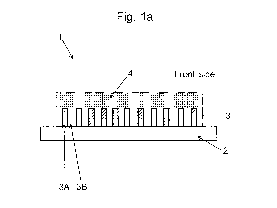
Figure 1 a shows a viewing region 1 of a security device having a transparent
substrate 2. One side of the substrate 2 comprises a layer of optical
interference
structure material 4, in this case a Bragg stack. Examples of tunable Bragg
stack
structures suitable for use with the current invention can be found in
W02009/143625.
Examples of alternative optical interference structure materials suitable for
use
with the present invention include thin film interference structures and
photonic
crystal structures. Thin film interference structures comprise repeating
layers of
different refractive indices, examples can include purely dielectric stacks
(metal
oxide or polymer) or those composed of alternate dielectric and metallic
layers.
Photonic crystal materials exhibit a periodic change in refractive index and,
according to the spatial variation in the refractive index, are classified as
one-
dimensional (1D), two-dimensional (2D) and three-dimensional (3D). 1D
photonic crystal structures correspond to thin film interference structures.
2D and
3D photonic crystal structures are structured optical materials in which the
refractive index varies periodically in two or preferably three dimensions.
These
materials exhibit a range of interesting optical effects when subject to
electromagnetic radiation of a wavelength comparable to the spatial modulation
CA 03019419 2018-09-28
WO 2017/168124 PCT/GB2017/050822
9
of the refractive index. Bragg reflection may occur over a range of
wavelengths
that depend on the direction of incidence/propagation and the periodicity of
refractive index variation. This gives rise to photonic "energy gaps" that are
analogous to the electronic band gaps in semiconductors. Typically,
electromagnetic waves within a certain frequency range cannot propagate in
particular directions within the crystal, and incident electromagnetic
radiation at
these wavelengths is consequently reflected. It is the presence of such
partial
photonic band gaps that gives rise to the angular dependent colour replay.
Referring back to Figure 1a, the layer of optical interference structure
material 4
is "backed" by a layer of at least partially light absorbing material, in this
case a
patterned screen 3 formed by an array of closely spaced fine lines 3A
separated
by spaces 3B (i.e. the screen pitch). In alternative, preferred embodiments,
the
screen is a fine dot screen, an example of which will be described with
reference
to Figure 2. As shown in Figures 1a-1c, the location of the material 4 and
screen
3 relative to the substrate may vary, since the substrate is transparent and
primarily serves to carry the device, without interfering with the incident
light or
the optical effects. In preferred embodiments, the screen is located between
the
substrate and the layer of optical interference structure material as shown in
Figure 1a.
When illuminated by incident light, the material 4 exhibits a strong
reflection
effect and the spectral reflectance of the material varies with the angle at
which it
is viewed, so that the part of the spectrum which is strongly reflected
changes as
the device is tilted in relation to the direction of the illuminating light.
In
transmitted white light, a complementary colour to the main reflected colour
is
observed with a similar colour change on tilting. The width of the lines 3A
and
the spacing 3B between the lines of the patterned opaque coating is preferably
non-resolvable such that the substrate appears a uniform colour which is the
colour of the particular wavelength reflected by the optical interference
structure
material 4 at any specific angle of view in reflective light but appears
uniformly
transparent in transmissive light to enable the complementary transmission
colours to be observed. The presence of the obscuring layer 3A enables the
reflected layer to dominate by absorbing sufficient light which is transmitted
CA 03019419 2018-09-28
WO 2017/168124 PCT/GB2017/050822
through the optical interference structure material 4 and which would
otherwise
overwhelm and conceal the optically variable effect.
The light absorbing material may comprise for example a black or other dark-
5 coloured material such as an ink and renders the overlying optical
interference
structure material visible in the second partial areas of the region by
absorbing
stray light other than that reflected by the material which would otherwise
overwhelm and conceal the optically variable effect. It will be appreciated,
however, that the light absorbing material need not absorb at all (UV and
visible)
10 wavelengths, and also need not absorb 100% of the light at those
wavelengths it
does absorb.
Advantageously, the light absorbing material absorbs at least 70% of incident
visible light, preferably at least 80%, more preferably at least 90%. Visible
light
is defined here as meaning all light with wavelengths between 350 nm and 800
nm, inclusive.
Advantageously the light absorbing material is additionally non-transparent
and
preferably transmits less than 30% of incident visible light in a single pass,
more
preferably less than 20%, still preferably less than 10%, most preferably is
substantially opaque.
Desirably, the light absorbing material is dark in colour, preferably black,
although alternatives such as dark blue or dark green are also envisaged. For
example, the light absorbing material may comprise an ink containing a dark
pigment such as carbon black. The light absorbing material may also comprise
a magnetic or electrically conductive substance, which may or may not be the
same pigment as that which gives the material its colour.
The light absorbing material preferably comprises a visually dark, e.g. grey
or
black, substance such as an ink. An example of a suitable light-absorbing
material which can be used in this and all other embodiments disclosed herein
would be an ink carrier, lacquer or binder containing a black or dark dye or
pigment such as the dye BASF Neozapon X51 or the pigment "carbon black 7"
CA 03019419 2018-09-28
WO 2017/168124 PCT/GB2017/050822
11
(well dispersed). The dye loading can be up to 50% (by weight) of the final
coat
of material depending on coat thickness and desired darkness.
Preferably, the absorbing layer is in the form of a screen. For example, the
absorbing layer pattern could be an array of dots or lines with sufficient
coverage
such that sufficient stray light other than that reflected by the optically
interference structure material which would otherwise overwhelm and conceal
the optically variable effect is absorbed while being sufficient sufficiently
transparent to enable the complementary colour to be viewable in transmitted
light. Non-linear screens are also envisaged. For example the screen could
comprise a circular or sinusoidal array of dots or lines. The screen can be
regular or stochastic.
Preferably, the coverage of the screen pattern is in the range 20-80%, and
more
preferably in the range 40-70% and even more preferably in the range 50-70%.
The width of the lines or the diameter of the dots forming the screen are
preferably in the range 100-300 pm and the spaces between the dots or lines
are also in the range 100-300 pm with values of each set chosen to achieve the
desired screen coverage. The absorbing pattern could be an array of dots or
lines with sufficient coverage to maintain the reflectivity of the optically
variable
material and therefore enable strong reflected colours, but sufficiently
transparent to enable transmitted colours. This is particularly appropriate
with a
polymeric substrate. Preferably, the screen is a regular array forming a
uniform
dot screen. Figure 2 shows a partial view of a uniform dot screen for use with
the
present invention. The geometry of the dots shown in Figure 2 corresponds to
50% coverage of the screen. In this example, the dots are filled squares with
a
side of 286 pm, and a pitch of 120 pm representing the distance between
adjacent squares.
The appropriate patterning of the obscuring layer may further provide a means
of
integrating "hidden" images or transmission designs. Figure 3 illustrates an
example where the optically variable device of the current invention is
incorporated into a transparent region of a paper substrate 40. In this
example,
most of the absorbing screen comprises an array of closely spaced fine lines
or
CA 03019419 2018-09-28
WO 2017/168124 PCT/GB2017/050822
12
dots as described with reference to Figures 1 or 2, but in the localised
regions
the absorbing coverage will be complete, i.e. substantially 100%, forming a
permanent image 31 which is revealed in transmitted light, as shown in Figure
3c. In an alternative embodiment, the absorbing screen will comprise a
permanent image formed by an appropriate patterning of the screen.
On viewing the device from the front side, illustrated in Figure 3, in
reflection
(Figure 3a) the authenticator will observe strong reflection colours. On the
front
side the numeral "500" is visible on the exposed polymeric film apart from in
the
aperture region where it is effectively concealed by the optical interference
structure material (typically it will only be present where the optically
variable film
is so will not be visible). On the rear side, numeral "500" is concealed by
the
complexity of the screen pattern but would be viewable on close examination in
reflection. When viewing the device in transmission (Figure 3c) the reflection
colours disappear and are replaced by the brighter transmission colours and
the
numeral "500" becomes visible as a silhouette image against the substantially
uniform coloured background. In this manner the optical interference structure
material is used to conceal a permanent image 31 in reflected light which is
then
revealed when image disappears on viewing in transmitted light.
In another embodiment of the invention the absorbing screen could be created
by using a light absorbing resist to pattern a metallised substrate using a
resist
and etch technique to create metallic screen elements superimposed with
absorbing screen elements. In effect this would be the method described in
EP1467873. The advantage of this is that from the front side the screen would
be dark and absorbing, but from the back side the screen would be metallic and
more attractive to the eye.
Embodiments of the invention are applicable to both paper and polymer
substrates and the permanent image can be applied by printing as well as
metallization or demetallisation techniques. Suitable printing techniques
include
lithography, UV cured lithography, intaglio, letterpress, flexographic
printing,
gravure printing or screen-printing. The permanent image must be sufficiently
opaque to appear as a silhouette in transmitted light. The permanent image can
CA 03019419 2018-09-28
WO 2017/168124 PCT/GB2017/050822
13
take any form such as patterns, symbols and alphanumeric characters and
combinations thereof. The indicia can be defined by patterns comprising solid
or
discontinuous regions which may include for example line patterns, fine
filigree
line patterns, dot structures and geometric patterns. Possible characters
include
those from non-Roman scripts of which examples include but are not limited to,
Chinese, Japanese, Sanskrit and Arabic. The permanent image may be single-
coloured or multi-coloured.
Security devices of the sorts described above can be utilised in many
different
ways. Preferably, in some cases the security device forms part of a security
article, such as a security thread, patch, foil or strip, for application to
or
incorporation into a security document. In other examples, the security device
may be formed directly on (i.e. integrally with) the security document.
The security device or article can be arranged either wholly on the surface of
the
base substrate of the security document, as in the case of a stripe or patch,
or
can be visible only partly on the surface of the document substrate, e.g. in
the
form of a windowed security thread. Security threads are now present in many
of
the world's currencies as well as vouchers, passports, travellers' cheques and
other documents. In many cases the thread is provided in a partially embedded
or windowed fashion where the thread appears to weave in and out of the paper
and is visible in windows in one or both surfaces of the base substrate. One
method for producing paper with so-called windowed threads can be found in
EP-A-0059056. EP-A-0860298 and WO-A-03095188 describe different
approaches for the embedding of wider partially exposed threads into a paper
substrate. Wide threads, typically having a width of 2 to 6mm, are
particularly
useful as the additional exposed thread surface area allows for better use of
optically variable devices, such as that presently disclosed.
The security device or article may be subsequently incorporated into a paper
or
polymer base substrate so that it is viewable from both sides of the finished
security substrate. Methods of incorporating security elements in such a
manner
are described in EP-A-1141480 and WO-A-03054297. In the method described
in EP-A-1141480, one side of the security element is wholly exposed at one
CA 03019419 2018-09-28
WO 2017/168124 PCT/GB2017/050822
14
surface of the substrate in which it is partially embedded, and partially
exposed
in windows at the other surface of the substrate.
Base substrates suitable for making security substrates for security documents
may be formed from any conventional materials, including paper and polymer.
Techniques are known in the art for forming substantially transparent regions
in
each of these types of substrate. For example, WO-A-8300659 describes a
polymer banknote formed from a transparent substrate comprising an opacifying
coating on both sides of the substrate. The opacifying coating is omitted in
localised regions on both sides of the substrate to form a transparent region.
In
this case the transparent substrate can be an integral part of the security
device
or a separate security device can be applied to the transparent substrate of
the
document. WO-A-0039391 describes a method of making a transparent region
in a paper substrate. Other methods for forming transparent regions in paper
substrates are described in EP-A-723501, EP-A-724519, WO-A-03054297 and
EP-A-1398174.
The security device may also be applied to one side of a paper substrate so
that
portions are located in an aperture formed in the paper substrate. An example
of a method of producing such an aperture can be found in WO-A-03054297.
An alternative method of incorporating a security element which is visible in
apertures in one side of a paper substrate and wholly exposed on the other
side
of the paper substrate can be found in WO-A-2000/39391.
Figure 4 shows a cross-sectional view of a further embodiment of the security
device of the current invention. In this example, the device is intended for
use as
a security label and comprises an inverse opal photonic crystal film 4. On the
front side of the photonic crystal film there are printed identifying indicia
5 using
inks or dyes. The integration of the optically variable effects such as
angular
dependent reflected colours with a permanent image including indicia not only
increases the aesthetics of the device but also makes it more memorable to the
general public. In the example illustrated, the optically variable effects are
used
to draw the attention of the viewer to the permanent image that can contain
important information such as the value of the protected document.