Note : Les descriptions sont présentées dans la langue officielle dans laquelle elles ont été soumises.
CA 03024955 2018-11-20
WO 2017/203441 PCT/IB2017/053056
"ELECTRICAL INTERCONNECTION SYSTEM BETWEEN AN INTRINSICALLY
EXTENSIBLE CONDUCTOR AND A NOT INTRINSICALLY EXTENSIBLE ONE"
********************
FIELD OF THE INVENTION
The present invention relates to a system for obtaining the electrical
interconnection between an intrinsically extensible conductor and a not
intrinsically
extensible one; in particular, the system of the invention finds application
in the
manufacture of devices implantable in the human or animal body, highly
conformable and deformable, for neurostimulation and/or neurorecording.
PRIOR ART
In many areas of the field there is a need to establish a stable electrical
connection between rigid or at most flexible conductors, such as wires or
tracks of
printed circuit boards, subjected to mechanical strains such as deformation,
vibration or compression. These strains generally act in directions transverse
to the
ideal line formed by the joining of the two conductors. The solutions
developed (also
object of patents) are focused on methods of reducing or cancelling the forces
on
the interface of the interconnection between the two conductors, to prevent
fractures
in the material that forms the conductor.
In recent years, conductors have been studied and are still under
development, which as well as being flexible are intrinsically extensible,
i.e. able to
undergo (reversible) lengthening in the direction of conduction of
electricity; while
being usable in any situation requiring a conductor, the primary intended
application
is for the production of electrodes implantable in the human (and animal)
body,
which requires that said electrodes can follow all the deformations of the
part in
which they are inserted, including lengthening and returns to the initial
length without
loss of continuity and of the main electrical characteristics.
A first method proposed to produce conductors with these characteristics
consists in preparing metal lines (wires or thin deposits) with undulating
pattern
within biocompatible elastomeric polymers, making one or more electrical
contacts
emerge to the surface of the polymer at predeset points depending on the
intended
application; when the polymer undergoes the lengthening, the wavy shape of the
1
CA 03024955 2018-11-20
WO 2017/203441 PCT/IB2017/053056
metal line allows the stretching or shortening thereof. Conductors of this
type are
described for example in patents US 7,085,605 B2 and US 7,265,298 B2.
A second approach is described in US patent 9,107,592 B2, and consists in
depositing (with known methods) metal tracks on a pre-stretched elastomer;
after
the deposit, the elastomer is left to return to its size "at rest" and the
metal deposit
is geometrically rearranged to follow the contraction thereof.
Finally, another alternative approach is described in the international patent
application WO 2011/121017 Al assigned to the present Applicant. According to
this method, the conductive line is created by implanting in an elastic
polymer
nanometric size aggregates of metals (for example, titanium); the examples
provided in the application show that although the deposit consists of
discrete
particles, electrical continuity is ensured, as well as its retention even
after tens of
thousands of cycles of lengthening/shortening of the conductor.
Conductors of this type, which can be stretched along the main direction of
electrical conduction, are referred to in the present text and in the claims
as
"intrinsically extensible", or even simply extensible.
The problems of creating contact points between different conductors,
mentioned above, are much more complex when one of the two conductors is
intrinsically extensible; similar problems are encountered if the two
conductors are
zo both of the intrinsically extensible type, but have a large difference
in the modulus
of elasticity.
The solutions traditionally adopted for connecting rigid or at most flexible
conductors are not suitable for these cases where, in addition to the
deformations
mentioned above, in the contact area there are also longitudinal deformations
due
to forces acting in opposite directions along the ideal line formed by the
joining of
the two conductors.
In fact, the interconnection between a soft and extensible conductive
structure
and a non-extensible one (such as a metal wire), connected to each other and
subjected to strains and deformations, is very critical because stresses
accumulate
mostly at this point, giving rise to mechanical failures and consequent power
disruptions.
The problem is further complicated by the fact that, with a view to the
2
CA 03024955 2018-11-20
WO 2017/203441 PCT/IB2017/053056
biomedical application, and particularly for implants in the human body, the
electrical
interconnection must be integrated into the smallest possible space and
possibly
even allow the interconnection of many contacts in parallel.
A possible solution (as described in Bossuyt F. et al, "Stretchable
Electronics
Technology for Large Area Applications: Fabrication and Mechanical
Characterization", IEEE Transactions on Components, Packaging and
Manufacturing Technology 3, no. 2 (February 2013): 229-35.
doi:10.1109/TCPMT.2012.2185792) is to integrate a rigid structure ("armour")
in the
interconnection region of the extensible part, so as to prevent mechanical
stress to
act on this area; the armour may for example be a non-extensible sheet
integrated
into the extensible substrate in the interconnection area or similar measures.
This
approach is however simply a way to bring the problem to the interconnection
between two rigid parts and, requiring the integration of an additional part
(armour)
into the device, it is not suitable to at the same time solve the problem of
reducing
the size of the interconnection; for this reason, the use of an armour is not
optimal
for manufacturing a medical device where miniaturization is a prerequisite.
Patent application US 2003/0233133 Al describes a system for the electrical
interconnection between an integrated circuit and conductive track on a
flexible
substrate; the system described in this document constitutes an improvement
over
zo previous systems, but does not allow the electrical connection with
conductive
tracks deposited on extensible substrates, as is necessary for the connection
of
implantable devices in the human or animal body in order to follow the
movements
thereof.
SUMMARY OF THE INVENTION
The object of the present invention is to provide a system for the creation of
a
stable electrical contact between an elastic and extensible conductor and a
non-
extensible one, or between two extensible conductors having different elastic
modulus, adapted to relieve stress in the interconnection region between the
two
conductors without using additional rigid armours.
This object is achieved with a system comprising:
- an interconnection board consisting of a non-extensible planar substrate
(flexible or rigid), on one functionalized face of which is present at least
one
3
CA 03024955 2018-11-20
WO 2017/203441 PCT/IB2017/053056
conductive track, each in electrical contact, at one end thereof, with at
least one
conductor external to the system which may be rigid, elastic or in its turn
extensible;
- an elastic and extensible substrate on a functionalized face of which is
present at least one extensible conductive structure;
- at least one deposit of an adhesive and electrically insulating material,
interposed between the interconnection board and elastic and extensible
substrate,
which adheres to said functionalized faces at least in part of the zones of
said faces
free from said at least one conductive track and said at least one extensible
conductive structure, establishing the adhesion between said board and
substrate
while allowing the relative motion thereof and ensuring the contact between
said at
least one conductive track and said at least one extensible conductive
structure,
optionally through at least one deposit of an adhesive, elastic and
electrically
conductive material.
BRIEF DESCRIPTION OF THE FIGURES
- Figures 1A, 1A' and 1B show sectional views of a system according to a first
embodiment of the invention;
- Figure 2 shows a perspective view of a system of Figures 1A, 1A' and 1B;
- Figures 3A and 3B show two sectional views of a system according to a
second embodiment of the invention;
- Figure 4 shows a perspective view of a system of Figures 3A and 3B;
- Figure 5 shows a sectional view of a particular embodiment of the
electrical
connection between the external conductor and the extensible conductive
structure;
- Figures 6 and 7 show two possible geometries of systems formed by
extensible substrates on which are present extensible conductive structures
connected to external conductors according to the invention.
DETAILED DESCRIPTION OF THE INVENTION
Features and advantages of the invention will be described in detail, with
reference to the figures, in the following description. In the figures, the
various parts
are not in scale and the widths of some areas, and especially the thickness of
some
layers, may be greatly increased for clarity of representation; in addition,
in all
figures, to like reference numerals correspond like elements.
The interconnection system of the invention allows obtaining a stable
electrical
4
CA 03024955 2018-11-20
WO 2017/203441 PCT/IB2017/053056
connection between an elastic and extensible substrate on which there is at
least
one extensible conductive structure and at least one external conductor; the
adhesive and electrically insulating material interposed between the
interconnection
board and the elastic and extensible substrate is in turn preferably elastic,
although
this is not a necessary condition for the implementation of the invention. The
elastic
and extensible substrate and the interconnection board generally have
conductive
structures on one face only; the faces of said board and said substrate on
which are
present the conductive structures are defined "functionalized faces" in the
present
description and in the claims.
A first embodiment of the interconnection system of the invention is shown in
Figures 1A and 1B. These Figures show views of the system in two mutually
orthogonal sections: in particular, the view in Figure lA is a section along
the dotted
line B-B' in Figure 1B, and the view in Figure 1B is a section along the
dotted line
A-A' in Figure 1A. Figure 1A shows, for simplicity, the connection between a
single
.. conductive track on the interconnection board and a single extensible
conductive
structure on the elastic and extensible substrate but, as described
hereinafter, the
interconnection systems of the invention typically connect multiple conductors
external to the system (hereinafter simply "external conductors") to multiple
extensible conductive structures; the most common case is that external
conductors
zo and extensible conductive structures are in equal number and connected
in a "one
to one" mode, but systems in multiplexing mode may also be implemented, in
which
multiple extensible conductive structures are contacted with a single external
conductor.
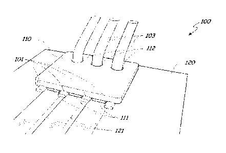
System 100 in Figures 1A and 1B consists of a planar and non-extensible
board 110 with a conductive track 111 on a functionalized face thereof; an
elastic
and extensible substrate 120, on a functionalized face of which is present the
extensible conductive structure 121 exposed on the surface of the substrate;
and at
least one deposit 101 of an electrically insulating, preferably elastic
adhesive
material interposed between said board 110 and substrate 120. Board 110 and
substrate 120 have the respective functionalized faces facing each other and
deposit 101 adheres to these functionalized faces. In practice, when board 110
and
substrate 120 are put in contact with each other, the presence of the
protruding track
5
CA 03024955 2018-11-20
WO 2017/203441 PCT/IB2017/053056
111 causes the formation of an empty space between the functionalized faces of
board and substrate, which is then filled with the material of deposit 101.
The
coupling between board 110 and substrate 120 through the material of deposit
101
is accomplished by applying a force (shown by arrows 500) that holds track 111
.. pressed against the extensible conductive structure 121, thus elastically
deforming
it along with substrate 120; this condition is shown in Figure 1A, which shows
how
substrate 120 and structure 121 are deformed by compression in the area in
contact
with track 111. In this way, the material of deposit 101 ensures the adhesion
between substrate and board, maintaining a residual pressure between track 111
.. and structure 121 even after removal of the force applied during assembly,
as shown
in Figure 1A'. In the preferred case in which deposit 101 is elastic, it also
ensures
that said track and said extensible conductive structure remain in contact
also in
case of their relative motions in the directions of the plane parallel to the
functionalized faces; these movements may be along a direction parallel to the
axis
of track 111 and structure 121, along a direction orthogonal to this axis, so
that track
111 and structure 121 move sideways relative to each other, or along
directions
which are combinations of these two main directions. The area covered by
deposits
101 is wide enough to absorb the stress generated during deformation of the
contact, without causing breakage thereof when the elastic and extensible
substrate
zo 120 is deformed to the normal elongation degrees to which it may be
subjected by
the movements of the human body following the implantation into the same.
At one end of board 110 (see Figure 1B) an external conductor 103 is present
for the electrical connection of the system with external devices, for example
an
electrical signal recording system or electrical stimulation system for
.. neurophysiology, in case of use of the extensible conductive structures as
electrodes for neuromodulation; this conductor may be of any type, for example
rigid, elastic but not extensible or in turn extensible; typically, the
external conductor
103 is an electric wire, for example made of copper. Conductor 103 is in
electrical
contact with track 111 through an opening 112 in board 110. The specific
methods
for establishing a connection between conductor 103 and track 111 through
opening
112 are illustrated below.
As mentioned above, Figures 1A, 1A' and 1B show a system in which a single
6
CA 03024955 2018-11-20
WO 2017/203441 PCT/IB2017/053056
interconnection is established between a track 111 and a conductive structure
121,
but the system of the invention is particularly useful to implement multiple
interconnections between multiple external conductors and multiple extensible
conductive structures, which may be in number equal to or different than the
external
conductors. Figure 2 shows a perspective view of an interconnection system
100;
in this figure, for simplicity, the mild depression of structures 121 at
tracks 111 is not
shown. There are three tracks 111 on board 110, in contact with as many
extensible
conductive structures 121 present on the elastic and extensible substrate 120;
the
three tracks are then connected to three external conductors 103, via through
holes
112 in board 110; the figure also shows the placement, in this embodiment of
the
interconnection system of the invention, of deposits 101.
For the production of the components of the system of the invention, all the
materials that have suitable physical and chemical properties may be used. As
examples, we may mention:
- for the construction of board 110, an electrically insulating material may
be
used, usually made of a polymeric material; the board may be rigid or
preferably
flexible, but non-extensible; typically, this board is of the same type as
those used
for the production of printed circuit boards (PCBs);
- tracks 111 are made of metal, for example copper, silver, gold, platinum or
zo cobalt-nickel based alloys, and may be deposited with any known
technique, such
as the technique of coating the whole face of the board with metal, masking
with
inks of the parts corresponding to the tracks to be produced, and selective
removal
of non-masked metal parts with chemical etchings (typically acid baths); or,
alternately, with selective deposition techniques through masking (e.g.
sputtering);
- for the elastic and extensible substrate 120, any elastomeric polymer
material
may be used; examples of such materials are polyurethane elastomers,
elastomeric
fluoropolymers, polyolefin-based elastomers, polybutadiene (BR), styrene-
butadiene rubbers (SBR), ethylene-propylene rubbers (EPR), ethylene-propylene-
diene rubbers (EPDM), nitrile rubbers (NBR), acrylic rubbers (ACM), the
rubbers
based on isobutylene and isoprene (IIR), and preferably silicones
(polysiloxanes);
- the extensible conductive structures 121 on the substrate are made by
implanting particles of conductive materials, typically metals (such as gold)
in the
7
CA 03024955 2018-11-20
WO 2017/203441 PCT/IB2017/053056
surface of the substrate; the preferred technique to achieve implantation is
"Supersonic Cluster Beam Implantation" or SCBI, described in patent
application
WO 2011/121017 Al assigned to the present Applicant;
- the adhesive material for making deposits 101 may be non-elastic, such as
an epoxy resin or another polymer; preferably, though, said material is
elastic and
is typically a silicone;
- finally, the external conductors 103 may be of any known type, for
example
a cable or a braid of metal covered with insulating material.
In a second embodiment, the system of the invention (200) further comprises
an additional deposit of an elastic, adhesive and electrically conductive
material,
interposed between the track on the board and the conductive structure on the
elastic and extensible substrate. This embodiment is shown in Figures 3A and
3B,
representing views in two mutually orthogonal sections similar to those in
Figures
lA and 1B (the view in Figure 3A is a section along the dotted line B-B' in
Figure 3B
and the view in Figure 3B is a section along the dotted line A-A' in Figure
3A); also
Figures 3A and 3B show, for convenience, only one interconnection between a
track
and an extensible conductive structure.
System 200 consists of a planar and non-extensible board 110 with a
conductive track 111 on a face thereof; an elastic and extensible substrate
120, on
zo a face of which is present the extensible conductive structure 121; and
at least one
deposit 101 of an electrically insulating, preferably elastic adhesive
material
interposed between the functionalized faces of said board 110 and substrate
120.
In this case, however, track 111 and the extensible conductive structure 121
are not
in direct contact with each other, but through a deposit 102 of an elastic,
adhesive
and electrically conductive material, that adheres to both cited elements and
ensures electrical continuity between them. With this configuration, the
electrical
contact between track 111 and conductive structure 121 is guaranteed, in
addition
to relative movements in the plane, also for small movements perpendicular to
the
plane of the functionalized faces, i.e. movements that move track 111 away
from
structure 121; moreover, this configuration increases the adhesion surface
(and thus
the adhesion strength) between board 110 and substrate 120.
The materials for producing a system of type 200 are the same as mentioned
8
CA 03024955 2018-11-20
WO 2017/203441 PCT/IB2017/053056
for the first embodiment; the same material used for deposits 101 is used for
the
production of deposits 102, but charged with conductive particles, typically
metallic
and preferably silver powder, to make the deposit electrically conductive.
Materials
useful for this purpose are described in US patent 7,537,712 B2, entitled
"Electrically
conductive silicone rubber composition".
Figure 4 shows a perspective view of a system 200, according to this second
embodiment; in this case too, three conductive paths are shown, each
consisting of
an external conductor 103, a track 111, a deposit 102 of elastic electricity
conductive
material, and an extensible conductive structure 121.
The connection between the external conductors 103 and tracks 111 can be
implemented by any means and technique known to the man skilled in the art,
such
as welding (thermal welding, laser welding, ultrasonic welding), soldering,
mechanical fastening or gluing with conductive glues of any kind. In a typical
embodiment, the connection is made by means of through holes ("via holes") 112
made on board 110, filled with a conductive material (e.g. tin) in which one
end of
conductor 103 is embedded. Alternatively, the method outlined in Figure 5 may
be
used. In this method, the interconnection between the extensible device and
conductor 103 is achieved with a double-face interconnection board, consisting
of a
planar non-extensible board 110 having conductive tracks made of Cu plated
with
zo Au on both its faces. On the lower face of board 110 (the one facing the
extensible
conductive structure 121) there are one or more first tracks 111; on the upper
face
of board 110 there are one or more second tracks 111'. Each second track 111'
is
connected to a first track 111 through a through hole 112 which is also coated
with
a metal (typically Au) inside, as shown in section in Figure 5. The external
conductor
103 is connected to the upper conductive track 111' through a deposit of
conductive
material 104 (such as tin). The extensible conductive structure 121 is
connected to
track 111 through a deposit 102 of elastic, adhesive and electrically
conducting
material which in this alternative embodiment is dispensed through the through
hole.
This ensures the electrical connection between structure 121 and the external
conductor 103, through the through holes 112, the upper tracks 111' and the
conductive material 104. A deposit 101 of an electrically insulating and
preferably
elastic adhesive material, interposed between board 110 and substrate 120
(and/or
9
CA 03024955 2018-11-20
WO 2017/203441 PCT/IB2017/053056
between board 110 and structure 121) ensures an additional mechanical coupling
between the connection board and the intrinsically extensible device.
In all cases, the external conductor can be welded to track 111 (or to track
111') or glued with a conductive paste or glue.
The system of the invention allows overcoming various problems in the
electrical connection between extensible and non-extensible parts. A solution
using
simply a conductive glue to put a non-extensible wire in electrical contact
with an
extensible conductive structure, that is, without using the interconnection
board of
the present invention, would not produce the same results. In fact, even if a
contact
manufactured in this way would be able to ensure an electrical contact in the
absence of mechanical stress, due to low contact surface available on the wire
and
the large discrepancy between the mechanical properties of the two glued
parts, in
the presence of said stress the system could easily break, because stress
builds up
at the interface with the contact wire. Moreover, this solution would be even
more
.. unstable towards twisting strains. Finally, if multiple contacts on the
same device
are to be implemented, a direct contact system, through the silicone glue
alone,
would become cumbersome and difficult to implement.
The inventors have instead surprisingly observed that these problems do not
occur with the system of the present invention, as this allows obtaining a
large
zo contact surface between the rigid (or non-extensible) conductor and the
extensible
one, so that the mechanical forces due to the relative motions of the two
parts are
distributed over a larger area, thereby preventing the localization of stress
on the
electrical contact and allowing the interconnection of many contacts to be
obtained
in an efficient manner.
In particular, it was observed that through the present invention, the system
remains under conditions of electrical conduction when the shear stress is
such as
to cause an elongation of at least 5% of the extensible part and stress builds
up
between the rigid wire and the elastic and extensible substrate.
Summing up, the following advantages and features are obtained with the
system of the invention:
1: an electrical contact can be obtained between at least one intrinsically
extensive conductive structure and a non-extensible conductive part, such as a
wire;
CA 03024955 2018-11-20
WO 2017/203441 PCT/IB2017/053056
2: a stable electrical contact can be maintained even when a shear stress is
applied to the system consisting of an extensible structure and a non-
extensible
part;
3: a stable electrical contact can be maintained even when a torque stress is
applied to the non-extensible part with respect to the extensible structure;
4: the interconnection system allows establishing electrical contacts in
parallel
between different intrinsically extensible conductive structures and the
respective
non-extensible parts (such as for example a multiplicity of wires);
5: the footprint of the entire interconnection is thin enough to make possible
the implementation of devices like neuromodulation electrodes, which must
generally be used in small areas of the human body.
The invention will be further described by the following examples.
EXAMPLE 1
This example refers to the production of a system of the invention consisting
of the union of an extensible conductive structure with copper conductive
wires; the
system, 600, is shown in Figure 6.
The elastic and extensible substrate 601 is 200 pm thick and is made of two-
component silicone rubber; it is obtained by dispersing on a glass support 1
gram
of liquid silicone (MED-6033 of the company NuSil Technology LLC, Carpinteria,
zo California, USA), spread by the spin coating technique and polymerized
for 30
minutes at 150 C according to the manufacturer's instructions.
Two extensible U-shaped metal tracks, 602 and 602', are obtained in the
substrate thus produced, placed the first one into the second one as shown in
the
figure. These tracks consist of 20 nm thick platinum deposits obtained through
SCBI,
as described in patent application WO 2011/121017 Al, protecting the substrate
using a metal mask (stencil mask) of the desired shape. Thereafter, a 150 nm
layer
of gold exactly overlapping that of platinum is implanted through SCBI using
the
same setup described above. The tracks are 0.7 mm wide and are mutually spaced
by 0.3 mm. The length of the outer U track is 21 mm, while the inner one is 18
mm.
The metal tracks thus obtained constitute the extensible conductive structures
of the
invention. The interconnection between the extensible metal tracks and the
conductive copper wires 103 is obtained with an interconnection board 110,
where
11
CA 03024955 2018-11-20
WO 2017/203441 PCT/IB2017/053056
the connection mode is the one described above with reference to Figure 5, and
consisting of a double-sided printed circuit board. Board 100 consists of a
polymeric
support made of FR4 (an epoxy resin reinforced with glass fibres, standard in
the
field) having a length of 2 mm, width of 4.5 mm and thickness of 0.1 mm, on
which
are arranged four conductive tracks (111, not shown in the figure) made of Cu
plated
with Au (size: 1.2 mm x 0.7 mm x 50 pm). The Cu/Au conductive tracks are
present
on both faces of the board. Each track is connected with the underlying one
through
a through hole 112, whose inner walls are in turn coated with Au. A silicon
glue (101)
consisting of two-component liquid silicone Nusil MED 6033 is distributed on
the
silicone rubber, interposed between one conductive track and the other. The
interconnection board is placed on the silicone substrate, so as to match the
four
lower tracks with the four end parts of the extensible conductive structures
602 and
602'. A force is applied to the interconnection board equal to 1 N, evenly
distributed
on the board surface and perpendicular to the surface itself, so as to press
it on the
silicone substrate.
This ensures both the electrical contact between the extensible tracks and the
Cu/Au conductive tracks of board 110, and the mechanical coupling between
board
and elastic and extensible silicone substrate by the adhesive material 101.
The force
that presses the interconnection board on the silicone substrate is maintained
as
zo long as necessary for the hardening of material 101, which is obtained
by baking in
a furnace at 70 C for 60 minutes.
Once material 101 has hardened, four copper wires (103) of 0.1 mm diameter
are connected by tin soldering to the four parts 111' of Cu/AI present on the
upper
surface of board 110, and in contact with tracks 111 through the gold present
in the
through holes 112; each of the four copper wires is electrically insulated
with a
polymer coating.
In this way, the interconnection between a non-extensible electrical conductor
(copper wire) and an intrinsically extensible electrical conductor (Pt/Au
tracks
deposited on silicone rubber), through an interconnection board is completed.
The
upper face of board 110 is coated with an epoxy resin (not shown in figure) in
order
to electrically insulate and mechanically reinforce the tin soldered area.
Each end of tracks 602 and 602' is connected to a copper wire. In order to
12
CA 03024955 2018-11-20
WO 2017/203441 PCT/IB2017/053056
check the hold of the electrical interconnection under mechanical stress, the
following is carried out: a potential difference of 1 V is applied between two
copper
wires interconnected to the two ends of the same extensible track and the
electrical
resistance of the system is measured. The device is subjected to tensile
stress,
holding it by the copper wires on the one end, and by end 603 of the silicone
substrate on the other. A resistance of about 200 0 is measured at rest. Under
tensile stress, resistance values of about 270 0, 390 0 and 880 0 are
observed, for
silicone substrate extensions equal to 5%, 10%, 20%, respectively. Returning
the
device to rest position, the resistance returns to a value of 200 O.
EXAMPLE 2
This example refers to the production of another system of the invention
consisting of the union of an extensible conductive structure with copper
conductive
wires; the system, 700, is shown in Figure 7.
The procedure outlined in Example 1 for the coupling between an elastic and
extensible substrate and an interconnection board 110 to which four copper
wires
103 are connected is repeated, with the only difference of the different
structure of
the extensible conductive structure.
The extensible part of the system consists of an elastic and extensible
substrate 701 on which four extensible metal tracks 702 of Au/Pt are present,
zo .. terminated by an electrode of Pt, 703, also extensible. In their
narrowest part (the
one closest to the interconnect board), the tracks are 0.7 mm wide and
mutually
spaced by 0.3 mm; the four tracks are 12, 22, 32 and 44 mm long, respectively.
The
Pt electrodes (703) are circular, with a diameter of 3.5 mm. The tracks are
made
through deposition of Pt and Au nanoparticles on a silicone rubber substrate
about
200 pm thick; substrate and tracks are produced as described in example 1. In
detail, the tracks are obtained by depositing a 20 nm Pt layer and then a 75
nm thick
Au layer; electrodes 703 are obtained by depositing 150 nm Pt and partially
overlaying the Pt/Au tracks on the Pt electrode to ensure electrical
continuity
between the two elements. The tracks and electrodes thus obtained constitute,
together with the silicone substrate, an intrinsically extensible conductive
composite
material.
After the coupling between board and extensible conductive structure, the
13
CA 03024955 2018-11-20
WO 2017/203441 PCT/IB2017/053056
entire system (except for the copper wires 103) is coated with a 200 pm thick
layer
of silicone rubber, leaving only the Pt electrodes exposed.
The device is immersed in a saline solution, keeping the free end of the
copper
wires outside the solution. A counter electrode is also added to the solution
consisting of a Pt rod and between the counter electrode and each of the four
extensible electrodes, one at a time, an electric current is flown by applying
a
potential difference of 1 V. The circuit impedance is measured and recorded
for each
of the four tracks 702; the measured values are 170, 175, 179 and 183 0,
respectively. In order to check the hold of the electrical interconnection to
mechanical fatigue, the device is then subjected to 1000 elongation cycles,
keeping
it on one end by the copper wires, and on the other end by the end (704) of
the
extensible structure that is furthest from the interconnection board. In each
cycle,
the extensible structure is stretched by 10% of its length at rest, and then
brought
back to the original length, at a rate of 1 mm/s. At the end of 1000 cycles,
the system
is again immersed into the saline solution, and the measurement of the four
impedance values is repeated, obtaining values of 175, 180, 182 and 191 0,
respectively, slightly higher than those recorded on the system immediately
after its
production; this demonstrates the mechanical fatigue strength of the
interconnection
between copper wires and extensible structure.
EXAMPLE 3
The procedure of Example 2 is repeated.
In this case, the four through holes 112 on board 110 are filled with
conductive
silicone CV 2644 (NuSil), prepared according to the manufacturer's
instructions; the
conductivity of conductive silicone is due to the presence of Ag particles
therein.
The conductive silicone is loaded into a syringe and dispensed within each via
through a needle. The conductive silicone fills hole 112, thus creating the
electrical
contact between the underlying extensible conductive track and the Cu/Au metal
conductive tracks of the interconnection board. The device is baked at 70 C
for one
hour, so as to cure the conductive silicone. On the resulting system,
following the
method of Example 2, impedance is measured for each of the four tracks and
four
electrical contacts 703, obtaining values of 173, 177, 182 and 185 O.
The system is then subjected to the same fatigue program of Example 2 (1000
14
CA 03024955 2018-11-20
WO 2017/203441 PCT/IB2017/053056
cycles of elongation by 10% of the length of the system at rest, and back to
the
original length, at a rate of 1 mm/s).
At the end of the fatigue program, the impedance is again measured for each
of the four tracks and four electrical contacts 703, obtaining values of 177,
180, 187
and 191 0 respectively, slightly higher than those registered on the system
just
produced, demonstrating the mechanical fatigue strength of the interconnection
between copper wires and extensible structure.