Note : Les descriptions sont présentées dans la langue officielle dans laquelle elles ont été soumises.
CA 03026329 2018-12-03
DESCRIPTION
POWER CONVERSION DEVICE
TECHNICAL FIELD
[0001]
The present invention relates to a power conversion device that converts power
output from an alternating-current power supply or a direct-current power
supply to
desired direct-current power.
BACKGROUND ART
[0002]
Conventionally, a power conversion device is used for charging a low-voltage
battery from a high-voltage battery, in an electric car, a hybrid vehicle, or
the like. A
switch is mounted inside the power conversion device, which is formed by a
power
semiconductor element of a discrete package or a modularized power
semiconductor
element (hereinafter, "power module"). The power module switches on/off of the
switch by a signal provided from a control circuit to convert a voltage.
[0003]
When a switching element is switched on and off, switching noise is generated
in the power module and propagates to the power-supply side and the load side.
Therefore, in a case where power is supplied from a commercial power supply
installed
in a standard home to a power conversion device mounted on a vehicle, for
example,
noise may propagate to an electric system on the home side.
[0004]
Patent Literature 1 discloses suppressing of noise by grounding a frame of a
reactor provided in a power module via an impedance element in order to remove
noise.
CITATION LIST
PATENT LITERATURE
1
=
[0005]
Patent Literature 1: Japanese Patent Laid-Open Publication No. 2006-238582
SUMMARY OF INVENTION
[0006]
However, the conventional example disclosed in Patent Literature 1 does not
adjust an impedance between an inductance element and the frame, and does not
reduce
noise effectively.
[0007]
The present invention has been made in view of such conventional problems. It
is an object of the present invention to provide a power conversion device
that can reduce
noise generated when a switching element is switched on and off.
[0008]
A power conversion device according to an aspect of the present invention
.. includes an inductance element connected to a first power feed bus, a
switching element
that converts power supplied between the first power feed bus and a second
power feed
bus by switching, a housing that houses the inductance element and the
switching element,
and a first impedance element provided between the inductance element and the
housing.
In one embodiment, the present invention provides a power conversion device
that converts power supplied from a first power feed bus and a second power
feed bus,
the power conversion device comprising:
an inductance element connected to the first power feed bus;
a switching element that converts power supplied between the first power feed
bus and the second power feed bus by switching;
2
CA 3026329 2020-03-09
a housing that houses the inductance element and the switching element
therein;
a first impedance element provided between the inductance element and the
housing; and
a second impedance element provided between the second power feed bus and
the housing,
wherein the first impedance element is electrically connected to the housing,
and
wherein the second impedance element is electrically connected to the housing.
In another embodiment, the present invention provides a power conversion
device
that converts power supplied from a first power feed bus and a second power
feed bus,
the power conversion device comprising:
an inductance element connected to the first power feed bus;
a switching element that converts power supplied between the first power feed
bus and the second power feed bus by switching;
a housing that houses the inductance element and the switching element
therein;
and
a first impedance element provided between the inductance element and the
housing, wherein
the first impedance element is a first capacitance element that is provided
between the inductance element and the housing in such a manner that an
electrostatic
capacitance between the inductance element and the housing, including a first
stray
capacitance between the inductance element and the housing, match with a
second stray
capacitance between the second power feed bus and the housing,
wherein the first impedance element is electrically connected to the housing.
In another embodiment, the present invention provides a power conversion
device
that converts power supplied from a first power feed bus and a second power
feed bus,
the power conversion device comprising:
2a
CA 3026329 2020-03-09
,
an inductance element connected to the first power feed bus;
a switching element that converts power supplied between the first power feed
bus and the second power feed bus by switching;
a housing that houses the inductance element and the switching element
therein;
and
a first impedance element provided between the inductance element and the
housing, wherein
the first impedance element is formed by a first capacitance element and a
first
resistance element,
wherein the first impedance element is electrically connected to the housing.
ADVANTAGEOUS EFFECTS OF INVENTION
[0009]
According to an aspect of the present invention, it is possible to reduce
noise
generated when a switching element is switched on and off.
BRIEF DESCRIPTION OF DRAWINGS
[0010]
[Fig. 1] Fig. 1 is a circuit diagram illustrating a configuration of a power
conversion device and peripheral devices thereof according to an embodiment of
the
present invention.
2b
CA 3026329 2020-03-09
CA 03026329 2018-12-03
[Fig. 2] Fig. 2 is an explanatory diagram illustrating a cross-section of an
inductance element and a second power feed bus of the power conversion device
according to a first embodiment.
[Fig. 3] Fig. 3 is a graph representing the level of noise generated in a
power
conversion device.
[Fig. 4] Fig. 4 is an explanatory diagram illustrating a cross-section of an
inductance element and a second power feed bus of a power conversion device
according to a modification of the first embodiment.
[Fig. 5] Fig. 5 is an explanatory diagram illustrating a cross-section of an
inductance element and a second power feed bus of a power conversion device
according to a second embodiment.
[Fig. 6] Fig. 6 is an explanatory diagram illustrating a cross-section of an
inductance element and a second power feed bus of a power conversion device
according to a modification of the second embodiment.
[Fig_ 7] Fig. 7 is an explanatory diagram illustrating a cross-section of an
inductance element and a second power feed bus of a power conversion device
according to a third embodiment.
[Fig. 8] Fig. 8 is an explanatory diagram illustrating a cross-section of an
inductance element and a second power feed bus of a power conversion device
according to a fourth embodiment.
[Fig. 9] Fig. 9 is an explanatory diagram illustrating a cross-section of an
inductance element and a second power feed bus of a power conversion device
according to a fifth embodiment.
[Fig. 10] Fig. 10 is a graph representing a relation between a frequency and
an
impedance of the power conversion device according to the fifth embodiment.
[Fig. 11] Fig. 11 is an explanatory diagram illustrating a cross-section of an
inductance element and a second power feed bus of a power conversion device
according to a sixth embodiment.
[Fig. 12] Fig. 12 is an explanatory diagram illustrating a cross-section of an
inductance element and a second power feed bus of a power conversion device
3
CA 03026329 2018-12-03
according to a seventh embodiment.
[Fig. 13] Fig. 13 is an explanatory diagram illustrating a cross-section of an
inductance element and a second power feed bus of a power conversion device
according to a modification of the seventh embodiment.
[Fig. 141 Fig. 14 is an explanatory diagram illustrating a cross-section of an
inductance element and a second power feed bus of a power conversion device
according to an eighth embodiment.
[Fig. 15] Fig. 15 is an explanatory diagram illustrating a cross-section of an
inductance element and a second power feed bus of a power conversion device
according to a ninth embodiment.
[Fig. 16] Fig. 16 is an explanatory diagram illustrating a cross-section of an
inductance element and a second power feed bus of a power conversion device
according to a tenth embodiment.
[Fig. 17] Fig. 17 is a graph representing a relation between a frequency and
an
impedance of the power conversion device according to the tenth embodiment.
[Fig. 181 Fig. 18 is a graph representing a relation between an impedance and
noise of the power conversion device according to the tenth embodiment.
[Fig. 19] Fig. 19 is an explanatory diagram illustrating a cross-section of an
inductance element and a second power feed bus of a power conversion device
according to a first modification of the tenth embodiment.
[Fig. 20] Fig. 20 is an explanatory diagram illustrating a cross-section of an
inductance element and a second power feed bus of a power conversion device
according to a second modification of the tenth embodiment.
[Fig. 21] Fig. 21 is an explanatory diagram illustrating a cross-section of an
25. inductance element and a second power feed bus of a power conversion
device
according to an eleventh embodiment.
[Fig. 22] Fig. 22 is a graph representing a relation between a frequency and
an
impedance of the power conversion device according to the eleventh embodiment.
[Fig. 23] Fig. 23 is a graph representing a relation between a frequency and
an
impedance of a power conversion device according to a first modification of
the
4
CA 03026329 2018-12-03
eleventh embodiment.
[Fig. 24] Fig. 24 is a graph representing a relation between a frequency and
an
impedance of a power conversion device according to a second modification of
the
eleventh embodiment.
[Fig. 25] Fig. 25 is a graph representing a relation between a frequency and
an
impedance of a power conversion device according to a third modification of
the
eleventh embodiment.
[Fig. 26] Fig. 26 is an enlarged view of a portion "A" illustrated in Fig. 25.
[Fig. 27] Fig. 27 is a graph representing a relation between a resistance
value
of each resistance element and a noise level in the power conversion device
according to
the eleventh embodiment.
[Fig. 28] Fig. 28 is a circuit diagram illustrating another configuration of a
power conversion device.
[Fig. 29] Fig. 29 is a circuit diagram illustrating further another
configuration
of a power conversion device.
DESCRIPTION OF EMBODIMENTS
[0011]
Embodiments of the present invention are described below with reference to
the accompanying drawings.
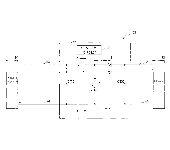
[Descriptions of first embodiment]
Fig. 1 is a circuit diagram illustrating a configuration of a power conversion
device and peripheral devices thereof according to a first embodiment of the
present
invention. As illustrated in Fig. 1, a power conversion device 101 according
to the
. 25 present embodiment is entirely covered by a housing 1 made of metal,
such as iron or
aluminum. The input side of the power conversion device 101 is connected to a
power
supply 91 that outputs a direct current via a first power feed bus 93 and a
second power
feed bus 94, and the output side thereof is connected to a load 92 via output
lines 95 and
96. Therefore, it is possible to convert a voltage supplied from the power
supply 91
into a desired voltage and supply the converted voltage to the load 92. The
power
5
CA 03026329 2018-12-03
supply 91 is a commercial power supply or a battery installed in a standard
home, for
example. The load 92 is a battery mounted on an electric car or a hybrid
vehicle, for
example.
[0012]
A positive terminal of the power supply 91 is connected to the first power
feed
bus 93, and a negative terminal thereof is connected to the second power feed
bus 94.
[0013]
An inductance element Li connected to the first power feed bus 93 is provided
in the housing I of the power conversion device 101. Further, a power module 3
is
provided between the first power feed bus 93 and the second power feed bus 94.
[0014]
The power module 3 includes a switching element Q1 such as an IGBT
(insulated gate bipolar transistor) or a MOSFET, and a diode DI. The
inductance
element LI is, for example, a toroidal winding coil or a flat coil.
[0015]
Smoothing capacitors C100 and C200 are provided at a preceding stage and a
subsequent stage of the power module 3, respectively. A control input of the
switching
element Q1 (for example, a base of an IGBT) is connected to a control circuit
2 that
controls on/off of the switching element Ql.
[0016]
By controlling on/off of the switching element Q1 under control by the control
circuit 2, a voltage supplied from the power supply 91 is converted to a
different voltage
to be supplied to the load 92.
[0017]
Fig. 2 illustrates an "A-Am cross-section illustrated in Fig. 1. As
illustrated in
Fig. 2, a first impedance element 11 is provided between the inductance
element Li' and
the housing 1. For example, the first impedance element 11 is a capacitance
element
or a series-connected circuit formed by a capacitance element and a resistance
element.
[0018]
In the power conversion device 101 according to the first embodiment, by
6
CA 03026329 2018-12-03
providing the first impedance element 11, an impedance between the inductance
element Li and the housing 1 is made closer to a second stray capacitance that
exists
between the second power feed bus 94 and the housing 1. In this manner, noise
propagating from the inductance element Li to the housing 1 is suppressed,
when
power is supplied to the load 92 illustrated in Fig. 1 to drive the load 92.
To "make
closer" is a concept including complete match.
[0019]
Fig. 3 is a graph representing noise that propagates to the housing 1 when the
switching element Q1 is switched. In Fig. 3, a curve Si illustrated with a
dotted line
represents a change of noise in a case where the first impedance element 11 is
not
provided, and a curve S2 illustrated with a solid line represents a change of
noise in a
case where the first impedance element 11 is provided. As is understood from
the
graph of Fig. 3, noise propagating from the inductance element Ll to the
housing 1 is
reduced by providing the first impedance element 11.
[0020]
In this manner, in the power conversion device according to the first
embodiment, an impedance between the inductance element Li and the housing 1
can
be made higher to become closer to a second stray capacitance existing between
the
second power feed bus 94 and the housing 1 by providing the first impedance
element
11. Therefore, noise propagating from the inductance element Li to the housing
1 can
be reduced.
[0021]
[Descriptions of modification of first embodiment]
Next, a modification of the first embodiment is described. A power
conversion device according to the modification is different in that it uses a
planer
inductance element LI a and the second power feed bus 94 is formed as a flat
wire or a
substrate pattern. Fig. 4 is a cross-sectional view of the inductance element
Lla and
the second power feed bus 94. As illustrated in Fig. 4, the inductance element
Li a and
the second power feed bus 94 both have a flat shape. Further, the first
impedance
element 11 is provided between the inductance element LI a and the housing 1.
The
7
CA 03026329 2018-12-03
planar inductance element Li a can be formed by a substrate pattern.
[0022]
Also with this configuration, it is possible to reduce noise that propagates
from
the inductance element Lla to the housing 1, similarly to the first embodiment
described above. Although each of the following embodiments will describe an
example in which a toroidal coil is used as the inductance element Li, as
illustrated in
Fig. 2, a planar inductance element Lla illustrated in Fig. 4 can be used.
[0023]
[Descriptions of second embodiment]
Next, a second embodiment of the present invention is described. Fig. 5 is an
explanatory diagram illustrating a cross-section of the inductance element Li
and the
second power feed bus 94 of a power conversion device according to the second
embodiment. As illustrated in Fig. 5, the inductance element Li is housed in a
frame 4
made of metal, such as iron or aluminum. The frame 4 is fixed to the housing 1
and is
in electrical conduction with the housing 1. The first impedance element 11 is
provided between the inductance element Li and the frame 4. That is, the
second
embodiment is different from the first embodiment described above in that the
inductance element Li is housed in the frame 4. Because the frame 4 is
provided
within the housing 1 and the first impedance element 11 is provided between
the
inductance element Li and the frame 4, the first impedance element 11 is
provided
between the inductance element Li and the housing 1.
[0024]
As described above, the inductance element Li is housed in the frame 4 in the
power conversion device according to the second embodiment. Therefore, noise
directly radiated from the inductance element Ll can be suppressed. Further,
by
providing the first impedance element 11, it is possible to increase an
impedance
between the inductance element Li and the frame 4, so that an impedance
between the
inductance element Li and the housing 1 can be made closer to a second stray
capacitance between the second power feed bus 94 and the housing 1. As a
result,
noise propagating from the inductance element Li to the housing 1 can be
reduced.
8
CA 03026329 2018-12-03
[0025]
[Descriptions of modification of second embodiment]
Next, a modification of the second embodiment is described. Fig. 6 is an
explanatory diagram illustrating a cross-section of the inductance element Li
and the
second power feed bus 94 of a power conversion device according to the
modification
of the second embodiment
[0026]
As illustrated in Fig. 6, the modification is different from the second
embodiment described above in that a bottom surface of the frame 4 that houses
the
inductance element Li therein and the housing 1 are connected to each other by
a wire 5.
That is, the housing 1 and the frame 4 are in conduction with each other by
the wire 5.
The housing 1 and the frame 4 are fixed by an insulating body or the like (not
illustrated). Even with this configuration, effects identical to those of the
second
embodiment described above can be achieved.
[0027]
[Descriptions of third embodiment]
Next, a third embodiment of the present invention is described. Fig. 7 is an
explanatory diagram illustrating a cross-section of the inductance element Li
and the
second power feed bus 94 of a power conversion device according to the third
embodiment. As illustrated in Fig. 7, in the power conversion device according
to the
third embodiment, the inductance element Ll is housed in the frame 4. Further,
the
first impedance element 11 is provided to cover the inductance element Ll. The
first
impedance element 11 is a dielectric body, for example.
[0028]
- The frame 4 is provided in the housing 1, and the first impedance element
11 is
*provided between the inductance element Ll and the franie 4. Further, because
the
frame 4 and the housing 1 are coupled to each other by a stray capacitance,
the first
impedance element 11 is provided between the inductance element Li and the
housing
1.
[0029]
9
CA 03026329 2018-12-03
Further, the housing 1 and the frame 4 are fixed by an insulating body or the
like (not illustrated). Because a stray capacitance exists between the frame 4
and the
housing 1, a predetermined electrostatic capacitance exists between the
inductance
element Li and the housing 1.
[0030]
hi this manner, in the power conversion device according to the third
embodiment, noise propagating from the inductance element Li to the housing 1
can be
reduced by making a predetermined electrostatic capacitance described above
closer to
a second stray capacitance between the second power feed bus 94 and the
housing 1.
[0031]
[Descriptions of fourth embodiment]
Next, a fourth embodiment of the present invention is described. Fig. 8 is an
explanatory diagram illustrating a cross-section of the inductance element Ll
and the
second power feed bus 94 of a power conversion device according to the fourth
embodiment. As illustrated in Fig. 8, in the power conversion device according
to the
fourth embodiment, the first impedance element 11 is provided between the
inductance
element Li and the housing 1. Further, a second impedance element 12 is
provided
between the second power feed bus 94 and the housing 1.
[0032]
By providing the first impedance element 11 and the second impedance
element 12, it is possible to make an impedance between the inductance element
Li and
the housing 1 and an impedance between the second power feed bus 94 and the
housing
1 closer to each other. Therefore, it is possible to reduce noise propagating
from the
inductance element Li to the housing 1 and noise propagating from the second
power
feed bus 94 to the housing 1.
" [0033]
Further, because the first impedance element 11 and the second impedance
element 12 are provided, fine adjustment of each impedance can be performed.
Therefore, it is possible to match an impedance between the inductance clement
Li and
the housing 1 and an impedance between the second power feed bus 94 and the
housing
CA 03026329 2018-12-03
1 more easily. Therefore, it is possible to reduce noise propagating from the
inductance element Li to the housing 1 and noise propagating from the second
power
feed bus 94 to the housing 1 with a simple operation.
[0034]
[Descriptions of fifth embodiment]
Next, a fifth embodiment of the present invention is described. Fig. 9 is an
=
explanatory diagram illustrating a cross-section of the inductance element Li
and the
second power feed bus 94 of a power conversion device according to the fifth
embodiment. As illustrated in Fig. 9, in the fifth embodiment, a first
capacitance
element C11 is provided between the inductance element Li and the housing 1.
Further, a second capacitance element C12 is provided between the second power
feed
bus 94 and the housing 1. That is, in the fifth embodiment, the first
impedance
element 11 illustrated in Fig. 8 is replaced with the first capacitance
element C11 and
the second impedance element 12 is replaced with the second capacitance
element C12.
Further, CO1 in Fig. 9 denotes a first stray capacitance between the
inductance element
Li and the housing 1, and CO2 denotes a second stray capacitance between the
second
power feed bus 94 and the housing 1.
[0035]
In the fifth embodiment, an electrostatic capacitance that is a total of the
first
stray capacitance CO1 and an electrostatic capacitance of the first
capacitance element
C11 and an electrostatic capacitance that is a total of the second stray
capacitance CO2
and an electrostatic capacitance of the second capacitance element C12 are
made closer
to each other by appropriately setting the electrostatic capacitances of the
first
capacitance element C11 and the second capacitance element C12. As a result,
it is
possible to match a voltage applied between the inductance element Li and the
housing
1 with a voltage applied between the second power feed bus 94 and the housing
1, so
that noise propagating from the inductance element Li and the second power
feed bus
94 to the housing I can be reduced.
[0036]
Fig. 10 is a graph representing a relation between a frequency and an
11
CA 03026329 2018-12-03
impedance. In Fig. 10, a curve S3 illustrated with a solid line represents a
change of
impedance between the inductance element LI and the housing 1 with respect to
a
change of frequency. A curve S4 illustrated with a dotted line represents a
change of
impedance between the second power feed bus 94 and the housing 1 with respect
to a
change of frequency. As is understood from the curves S3 and S4, the
impedances
respectively represented by the curves S3 and S4 are substantially matched
with each
other irrespective of the frequencies thereof. That is, in the power
conversion device
according to the fifth embodiment, noise propagating to a housing can be
reduced even
in a case where a frequency of the switching element Q1 is changed.
[0037]
[Descriptions of sixth embodiment]
Next, a sixth embodiment of the present invention is described. Fig. 11 is an
explanatory diagram illustrating a cross-section of the inductance element Li
and the
second power feed bus 94 of a power conversion device according to the sixth
embodiment. As illustrated in Fig. 11, in the sixth embodiment, the first
capacitance
element C11 is provided between the inductance element Li and the housing 1,
similarly to the fifth embodiment illustrated in Fig. 9. Further, the second
capacitance
element C12 is provided between the second power feed bus 94 and the housing
1.
Further, the first stray capacitance CO1 exists between the inductance element
Ll and
the housing 1, and the second stray capacitance CO2 exists between the second
power
feed bus 94 and the housing 1. The sixth embodiment is different from the
fifth
embodiment in that the second power feed bus 94 is formed by a flat wire.
[0038]
In the power conversion device according to the sixth embodiment, an
electrostatic capacitance that is a total of the first stray . capacitance CO1
and an
electrostatic capacitance of the first capacitance element C11 and an
electrostatic
capacitance that is a total of the second stray capacitance CO2 and an
electrostatic
capacitance of the second capacitance element C12 can be made closer to each
other by
appropriately setting the electrostatic capacitances of the first capacitance
element Cll
and the second capacitance element C 12, similarly to the fifth embodiment
described
12
CA 03026329 2018-12-03
above. Use of a flat wire as the second power feed bus 94 enables adjustment
of the
second stray capacitance CO2. This point is described in detail below.
[0039]
An electrostatic capacitance between the second power feed bus 94 and the
housing 1 (the second stray capacitance CO2) can be expressed by the following
expression (1).
(Electrostatic capacitance) =c0=Er(S/d) = = -(1)
where 60 is a permittivity of vacuum, a is a relative permittivity, S is an
opposed area, and d is a distance.
[0040]
Therefore, by changing the opposed area S, it is possible to change the second
stray capacitance CO2 between the second power feed bus 94 and the housing 1.
In the
sixth embodiment, an electrostatic capacitance between the inductance element
Li and
the housing 1 and the electrostatic capacitance between the second power feed
bus 94
and the housing 1 are set by adjusting the opposed area S between the second
power
feed bus 94 and the housing 1 in addition to the first capacitance element C11
and the
second capacitance element C12. Therefore, adjustment of electrostatic
capacitances
can be easily performed. Accordingly, it is possible to make a voltage applied
between
the inductance element Li and the housing 1 and a voltage applied between the
second
power feed bus 94 and the housing 1 closer to each other, so that noise
propagating to
the housing I can be reduced.
[0041]
[Descriptions of seventh embodiment]
Next, a seventh embodiment of the present invention is described. Fig. 12 is
an explanatory diagram illustrating a cross-section of the inductance element
Li and the
= second power feed bus 94 of a power conversion 'device according to the
seventh
embodiment. As illustrated in Fig. 12, in the seventh embodiment, the first
capacitance element C11 is provided between the inductance element Li and the
housing 1, similarly to the fifth embodiment illustrated in Fig. 9. Further,
the second
capacitance element C12 is provided between the second power feed bus 94 and
the
13
CA 03026329 2018-12-03
housing 1. Further, the first stray capacitance CO1 exists between the
inductance
element Li and the housing 1, and the second stray capacitance CO2 exists
between the
second power feed bus 94 and the housing 1. The seventh embodiment is
different
from the fifth embodiment in that the housing 1 near the second power feed bus
94 is
formed by a thick portion 7.
[0042]
In the power conversion device according to the seventh embodiment, an
electrostatic capacitance that is a total of the first stray capacitance CO1
and an
electrostatic capacitance of the first capacitance element C11 can be made
closer to an
electrostatic capacitance that is a total of the second stray capacitance CO2
and an
electrostatic capacitance of the second capacitance element Cl2 by
appropriately setting
the electrostatic capacitances of the first capacitance element C11 and the
second
capacitance element C12. In this case, the second stray capacitance CO2 can be
adjusted by changing the thickness of the thick portion 7.
[0043]
That is, it is possible to change the second stray capacitance CO2 between the
second power feed bus 94 and the housing 1 by changing the distance d, as
expressed by
the expression (1) described above. In the seventh embodiment, an
electrostatic
capacitance between the inductance element Li and the housing 1 is matched
with an
electrostatic capacitance between the second power feed bus 94 and the housing
1 by
adjusting the thickness of the thick portion 7 in addition to the first
capacitance element
C11 and the second capacitance element C12. Therefore, adjustment of
electrostatic
capacitances can be easily performed. Although Fig. 12 illustrates an example
in
which the thickness of the housing 1 is changed, the distance d can be changed
by
arranging a conductive plate member on an inner surface of the housing 1.
[0044]
Accordingly, it is possible to make a voltage applied between the inductance
element Li and the housing 1 and a voltage applied between the second power
feed bus
94 and the housing 1 closer to each other, so that noise propagating to the
housing 1 can
be reduced.
14
CA 03026329 2018-12-03
[0045]
[Descriptions of modification of seventh embodiment]
Next, a modification of the seventh embodiment of the present invention is
described. Fig. 13 is an explanatory diagram illustrating a cross-section of
the
inductance element Li and the second power feed bus 94 of a power conversion
device
according to the modification of the seventh embodiment. As illustrated in
Fig. 13, a
plate member 6 made of metal is provided on a portion of the inner surface of
the
housing 1, which is close to the second power feed bus 94, in the
modification.
Therefore, the second stray capacitance CO2 can be adjusted by changing a
distance
between the second power feed bus 94 and the plate member 6, similarly to the
seventh
embodiment described above, so that it is possible to make an electrostatic
capacitance
that is a total of the inductance element Li and the housing 1 and an
electrostatic
capacitance that is a total of the second power feed bus 94 and the housing 1
closer to
each other with a simple operation.
[0046]
[Descriptions of eighth embodiment]
Next, an eighth embodiment of the present invention is described. Fig. 14 is
an explanatory diagram illustrating a cross-section of the inductance element
LI and the
second power feed bus 94 of a power conversion device according to the eighth
embodiment. As illustrated in Fig. 14, in the eighth embodiment, the first
capacitance
element C11 is provided between the inductance element Li and the housing 1,
similarly to the fifth embodiment illustrated in Fig. 9. Further, the second
capacitance
element C12 is provided between the second power feed bus 94 and the housing
1.
[0047]
The eighth embodiment is different from the fifth embodiment in that a second
= dielectric body 8 is provided between the second power feed bus 94 and
the housing 1.
The first stray capacitance CO1 exists between the inductance element Ll and
the
housing 1, and the second stray capacitance CO2 exists between the second
power feed
bus 94 and the housing 1. The second stray capacitance CO2 is changed by a
permittivity of the second dielectric body 8.
CA 03026329 2018-12-03
[0048]
In the power conversion device according to the eighth embodiment, it is
possible to make an electrostatic capacitance that is a total of the first
stray capacitance
CO1 and an electrostatic capacitance of the first capacitance element C11 and
an
electrostatic capacitance that is a total of the second stray capacitance CO2
and an
electrostatic capacitance of the second capacitance element C12 closer to each
other by
appropriately setting the electrostatic capacitances of the first capacitance
element C11
and the second capacitance element C12. The second stray capacitance CO2 can
be
adjusted by changing a permittivity of the second dielectric body 8.
[0049]
That is, it is possible to change the second stray capacitance CO2 between the
second power feed bus 94 and the housing 1 by changing the relative
permittivity Er, as
expressed by the expression (1) described above. In the eighth embodiment, an
electrostatic capacitance between the inductance element Li and the housing 1
is
.. matched with an electrostatic capacitance between the second power feed bus
94 and
the housing 1 by adjusting the relative permittivity Er of the second
dielectric body 8 in
addition to the first capacitance element C11 and the second capacitance
element C12.
Therefore, adjustment of electrostatic capacitances can be easily performed.
[0050]
[Descriptions of ninth embodiment]
Next, a ninth embodiment of the present invention is described. Fig. 15 is an
explanatory diagram illustrating a cross-section of the inductance element Li
and the
second power feed bus 94 of a power conversion device according to the ninth
embodiment. As illustiated in Fig. 15, in the ninth embodiment, the first
capacitance
element C11 is provided between the inductance element Li and the housing 1,
similarly to the fifth embodiment illustrated in Fig. 9. Further, the second
capacitance
element C12 is provided between the second power feed bus 94 and the housing
1.
[0051]
The ninth embodiment is different from the fifth embodiment in that a first
dielectric body 9 is provided between the inductance element Li and the
housing 1 and
16
CA 03026329 2018-12-03
the second dielectric body 8 is provided between the second power feed bus 94
and the
housing I. The first stray capacitance CO1 exists between the inductance
element Li
and the housing 1, and the second stray capacitance CO2 exists between the
second
power feed bus 94 and the housing 1. The first stray capacitance CO1 is
changed by a
permittivity of the first dielectric body 9, and the second stray capacitance
CO2 is
changed by a permittivity of the second dielectric body 8.
[0052]
In the power conversion device according to the ninth embodiment, an
electrostatic capacitance that is a total of the first stray capacitance CO1
and an
electrostatic capacitance of the first capacitance element C11 and an
electrostatic
capacitance that is a total of the second stray capacitance CO2 and an
electrostatic
capacitance of the second capacitance element C12 are made closer to each
other by
appropriately setting the electrostatic capacitances of the first capacitance
element C11
and the second capacitance element C12. In this case, the first stray
capacitance CO1
and the second stray capacitance CO2 can be adjusted by changing
permittivities of the
first dielectric body 9 and the second dielectric body 8.
[0053]
That is, it is possible to change the first stray capacitance COI and the
second
stray capacitance CO2 by changing the relative permittivity Er in the
expression (1)
described above. In the ninth embodiment, an electrostatic capacitance between
the
inductance element Li and the housing 1 is matched with an electrostatic
capacitance
between the second power feed bus 94 and the housing 1 by adjusting the
relative
permittivity Er of the first dielectric body 9 and that of the second
dielectric body 8 in
addition to the first capacitance element C11 and the second capacitance
element C12.
Therefore, adjustment of electrostatic capacitances can be easily performed.
[0054]
[Descriptions of tenth embodiment]
Next, a tenth embodiment of the present invention is described. Fig. 16 is an
explanatory diagram illustrating a cross-section of the inductance element Li
and the
second power feed bus 94 of a power conversion device according to the tenth
17
CA 03026329 2018-12-03
embodiment. As illustrated in Fig. 16, in the tenth embodiment, a series-
connected
circuit formed by the first capacitance element C11 and a first resistance
element R11 is
provided between the inductance element Li and the housing 1. Further, the
second
capacitance element C12 is provided between the second power feed bus 94 and
the
housing 1.
[0055]
The first stray capacitance CO1 exists between the inductance element Li and
the housing 1, and the second stray capacitance CO2 exists between the second
power
feed bus 94 and the housing 1.
[0056]
In the power conversion device according to the tenth embodiment, a
combined impedance of the first stray capacitance CO1 and the series-connected
circuit
formed by the first capacitance element C11 and the first resistance element
R11
(hereinafter, this combined impedance is referred to as "first impedance") is
made closer
to a combined impedance of the second stray capacitance CO2 and an
electrostatic
capacitance of the second capacitance element C12 (hereinafter, this combined
impedance is referred to as "second impedance") by appropriately setting a
resistance
value of the first resistance element R11, an electrostatic capacitance of the
first
capacitance element C11, and the electrostatic capacitance of the second
capacitance
element C12.
[0057]
Further, a resonance frequency (referred to as "first resonance frequency")
exists between the inductance element Li and the housing 1 because of
existence of the
first capacitance element ClI, the first stray capacitance COI, and the
inductance
element Li. Therefore, in a case where the first resistance element RII is not
provided,
a first impedance is reduced at a first resonance frequency, so that a
difference between
the first impedance and a second impedance is enlarged, causing generation of
noise.
In the present embodiment, reduction of the first impedance is prevented by
providing
the first resistance element R11. This point is described in detail below.
[0058]
18
CA 03026329 2018-12-03
Fig. 17 is a graph representing a relation between a frequency and an
impedance. A curve Z2 (solid line) illustrated in Fig. 17 represents a change
of a
second impedance Z2 between the second power feed bus 94 and the housing I.
[0059]
A curve ZO (alternate long and short dash line) represents a change of the
first
impedance in a case where the first resistance element R11 is not provided in
Fig. 16,
that is, the inductance element LI and the housing 1 are connected to each
other by the
first capacitance element C 1 1. As represented by the curve ZO, a first
resonance
frequency M exists between the inductance element LI and the housing I, at
which the
impedance is significantly reduced.
[0060]
The first resonance frequency 10 described above can be expressed by the
following expression (2).
[Equation 1]
1
fo = (2)
2 L.FTT1-71
In the present embodiment, reduction of the first impedance at the first
resonance frequency M is suppressed by providing the first resistance element
R11.
[0061]
Specifically, the resistance value of the first resistance element R11 is set
to a
value that is larger than an impedance ZO(10) at the frequency M and is
smaller than the
second impedance Z2(10). That is, the resistance value of the first resistance
element
R11 is set in a range expressed by the following expression (3).
Z0(10)R11_2(10) ¨(3)
where ZO is an impedance by the inductance element LI, the first capacitance
element C11, and the first stray capacitance C01, and Z2 is an impedance by
the second
power feed bus 94, the second capacitance element C12, and the second stray
capacitance CO2. In the following descriptions, an element and a numerical
value of
19
CA 03026329 2018-12-03
that element are denoted by the same sign. For example, the resistance value
of the
resistance element R11 is denoted by the same sign R11.
[0062]
As a result, the first impedance at the first resonance frequency ft) can be
made
higher than the lowest point of the impedance ZO. Further, by making the
resistance
value R11 closer to Z2(f0), a change of the first impedance with respect to a
frequency
becomes a change as illustrated by a curve Z1 (dotted line) in Fig. 17, so
that the change
of the first impedance can be made closer to the curve Z2.
[0063]
That is, the resistance value of the first resistance element R11 is set to be
equal to or lower than an impedance between the second power feed bus 94 and
the
housing 1 at the first resonance frequency f0 and be higher than an impedance
between
the inductance element Ll and the housing 1 in a case where the first
resistance element
R11 is not included. Preferably, the resistance value of the first resistance
element R11
is set to match with the impedance between the second power feed bus 94 and
the
housing 1 at the first resonance frequency Et
[0064]
Therefore, at the first resonance frequency fO, it is possible to prevent
rapid
reduction of the first impedance, so that noise propagation to the housing 1
can be
reduced without being influenced by a change of frequency.
[0065]
Fig. 18 is a graph representing an effect of suppressing noise that propagates
to
the housing 1 at the first resonance frequency f0. The horizontal axis
represents a
magnitude of the first resistance element R11, and the vertical axis
represents a noise
level. As is understood from Fig. 18, by setting the resistance value R11 in a
range
from ZO(f0) to Z2(f0) (that is, a range expressed by the expressiorY (3)
described above),
the noise level can be reduced, and the effect of suppressing noise can be
increased as
R11 becomes closer to 22(f0).
[0066]
In this manner, in the tenth embodiment, a series-connected circuit formed by
CA 03026329 2018-12-03
the first capacitance element C11 and the first resistance element R11 is
provided
between the inductance element Li and the housing 1. Therefore, even in a case
where the first resonance frequency f0 exists between the inductance element
Li and
the first capacitance element C11, it is possible to prevent reduction of the
first
impedance at the first resonance frequency by setting the resistance value of
the first
resistance element R11 in the range of the expression (3) described above.
Consequently, it is possible to make a voltage applied between the inductance
element
Li and the housing 1 and a voltage applied between the second power feed bus
94 and
the housing 1 closer to each other, so that noise propagating to the housing 1
can be
reduced.
[0067]
In particular, noise can be reduced more effectively by matching the
resistance
value R11 with the impedance Z2(f0) between the second power feed bus 94 and
the
housing 1 at the first resonance frequency f0.
[0068]
[Descriptions of first modification of tenth embodiment]
Next, a first modification of the tenth embodiment is described. Fig. 19 is an
explanatory diagram illustrating a cross-section of the inductance element Ll
and the
second power feed bus 94 of a power conversion device according to the first
modification of the tenth embodiment.
[0069]
As illustrated in Fig. 19, the inductance element Ll is housed in the frame 4
made of metal, such as iron or aluminum. The frame 4 is connected to the
housing 1
by the wire 5. A series-connected circuit formed by the first resistance
element R11
and the first capacitance element C11 is provided between the inductance
element Li
and the frame 4.
[0070]
According to this configuration, the inductance element Li is housed in the
frame 4, thereby suppressing noise directly radiated from the inductance
element Li.
Further, by providing the first resistance element R11 and the first
capacitance element
21
CA 03026329 2018-12-03
C 1 1 within the frame 4, it is possible to make an impedance between the
inductance
element Li and the frame 4 higher, so that an impedance between the inductance
element Li and the housing 1 can be made closer to an electrostatic
capacitance
between the second power feed bus 94 and the housing 1 (an electrostatic
capacitance
that is a total of the second capacitance element C12 and the second stray
capacitance
CO2).
[0071]
Further, by appropriately setting the resistance value of the first resistance
element R11 similarly to the tenth embodiment described above, reduction of
the first
impedance at the first resonance frequency f0 can be prevented, and noise
propagating
from the inductance element Li to the housing 1 can be suppressed.
[0072]
[Descriptions of second modification of tenth embodiment]
Next, a second modification of the tenth embodiment is described. Fig. 20 is
an explanatory diagram illustrating a cross-section of the inductance element
L1 and the
second power feed bus 94 of a power conversion device according to the second
modification of the tenth embodiment.
[0073]
As illustrated in Fig. 20, the inductance element Li is housed in the frame 4
made of metal, such as iron or aluminum. A series-connected circuit formed by
the
first resistance element R11 and the first capacitance element C11 is provided
between
the inductance element Li and the frame 4. Further, the frame 4 and the
housing 1 are
insulated from each other. The first stray capacitance CO1 exists between the
frame 4
and the housing 1.
[0074]
Also in the second modification, the inductance element Li is housed in the
frame 4, similarly to the first modification described above. Therefore, noise
directly
radiated from the inductance element Li can be suppressed. Further, by
providing the
first resistance element R11 and the first capacitance element C11 within the
frame 4, an
.. impedance between the inductance element Li and the frame 4 can be
increased. As a
22
CA 03026329 2018-12-03
result, it is possible to make an impedance between the inductance element Li
and the
housing 1 closer to an electrostatic capacitance between the second power feed
bus 94
and the housing 1 (the electrostatic capacitance that is a total of the second
capacitance
element Cl2 and the second stray capacitance CO2).
[0075]
Further, by appropriately setting the resistance value of the first resistance
element R11 similarly to the tenth embodiment described above, reduction of
the first
impedance at the first resonance frequency f0 can be prevented, and noise
propagating
from the inductance element Li to the housing 1 can be suppressed.
[0076]
[Descriptions of eleventh embodiment]
Next, an eleventh embodiment of the present invention is described. Fig. 21
is an explanatory diagram illustrating a cross-section of the inductance
element Li and
the second power feed bus 94 of a power conversion device according to the
eleventh
IS embodiment. As illustrated in Fig. 21, in the eleventh embodiment, a
series-connected
circuit formed by the first capacitance element C11 and the first resistance
element R.11
is provided between the inductance element Li and the housing 1. Further, a
series-connected circuit formed by a second resistance element R12 and the
second
capacitance element C12 is provided between the second power feed bus 94 and
the
housing 1.
[0077]
In the power conversion device according to the eleventh embodiment, a first
impedance between the inductance element Li and the housing 1 and a second
impedance between the second power feed bus 94 and the housing I are made
closer to
each other by appropriately setting a resistance value of the first resistance
element R11,
an electrostatic capacitance of the first capacitance element C11, a
resistance value of
the second resistance element R12, and an electrostatic capacitance of the
second
capacitance element C 12_
[0078]
A method of setting the resistance values of the first resistance element R11
23
CA 03026329 2018-12-03
and the second resistance element R12 is described below. Fig. 22 is a graph
representing a relation between a frequency and an impedance. A curve Z11(f)
illustrated in Fig. 22 represents an impedance between the inductance element
Li and
the housing 1 in a case where the first resistance element R11 is not provided
(first
impedance), and a curve Z21(f) represents an impedance between the second
power
feed bus 94 and the housing 1 in a case where the second resistance element
R12 is not
provided (second impedance).
[0079]
Further, a curve Z10(f) represents an impedance of the inductance element Li,
and a curve Z20(f) represents an impedance of the second power feed bus 94.
Because
the curve Z10(f) only represents an inductance, the impedance increases with
increase
of a frequency. As for the curve Z20(f), the impedance is reduced with
increase of a
frequency, because of existence of a stray capacitance.
[0080]
Meanwhile, the impedance Z11(f) and the impedance Z2 1(f) have resonance
frequencies, respectively. Although it is desirable that both resonance
frequencies
match with each other, the resonance frequencies are different in many cases.
Here, it
is assumed that the resonance frequency of the impedance Z11(f) is a first
resonance
frequency fl and the resonance frequency of the impedance Z21(f) is a second
.. resonance frequency e.
[0081]
Therefore, as illustrated in Fig. 22, Z11 (f) and Z21(f) each have
characteristics
in which the impedance is rapidly reduced at the first resonance frequency fl
or the
second resonance frequency 2. In the present embodiment, resistance values of
the
first resistance element R11 and the second resistance element R12 are set in
such a
manner that reduction of the first impedance and the second impedance is
suppressed at
the respective resonance frequencies fl and 2.
[0082]
A range of the resistance value Rll and a range of the resistance value R12
are
set as expressed by the following expressions (4) and (5).
24
CA 03026329 2018-12-03
Z11(fl)R11.5221(f1) = (4).
Z21(f2) .sR12.11 (f2) = = = (5).
Specifically, the range of the resistance value R11 is set to a range denoted
by
a sign ql in Fig. 22, and the range of the resistance value R12 is set to a
range denoted
by a sign q2.
[0083]
By setting the resistance value of the first resistance element R11 to be in
the
range expressed by the expression (4) described above, it is possible to
suppress
reduction of the impedance of the curve Z11(1) in Fig. 22 at the first
resonance
frequency fl. Similarly, by setting the resistance value of the second
resistance
element R12 to be in the range expressed by the expression (5) described
above, it is
- possible to suppress reduction of the impedance of the curve Z21(f) at the
second
resonance frequency 12.
[0084]
That is, when a resonance frequency by the second power feed bus 94 and an
electrostatic capacitance of the second capacitance element C12 is assumed as
the
second resonance frequency 12, the resistance value of the second resistance
element
R12 is set to be higher than the impedance Z21(12) between the second power
feed bus
94 and the housing 1 and be lower than the impedance Z11(f2) between the
inductance
element Li and the housing 1, at the second resonance frequency 12 in a case
where the
second resistance element R12 is not included.
[0085]
Therefore, by providing the resistance elements R11 and R12, it is possible to
suppress reduction of the first impedance and the second impedance at the
first
resonance frequency fl and the second resonance frequency 12, and to prevent
generation of noise.
[0086]
Fig. 27 is a characteristic diagram illustrating a relation between a
resistance
value and a noise level, in which the horizontal axis represents a resistance
value and
the vertical axis represents a noise level. By setting the resistance values
R11 and R12
CA 03026329 2018-12-03
as expressed by the expressions (4) and (5) described above, the resistance
values are
values in a range denoted by a sign X1 . Therefore, the noise level can be
reduced.
[0087]
As described above, in the eleventh embodiment, a series-connected circuit
formed by the first capacitance element C11 and the first resistance element
R11 is
provided between the inductance element Li and the housing 1, and a series-
connected
circuit formed by the second capacitance element C12 and the second resistance
element R12 is provided between the second power feed bus 94 and the housing
1.
Therefore, it is possible to suppress reduction of the first impedance and the
second
impedance at the first resonance frequency fl and the second resonance
frequency f2, so
that noise propagating to the housing 1 can be reduced.
[0088]
Further, by setting the resistance values R11 and R12 as expressed by the
expressions (4) and (5) described above, it is possible to suppress reduction
of the
impedance at the first resonance frequency fl and the second resonance
frequency f2, so
that noise propagating to the housing 1 can be reduced.
[0089]
[Descriptions of first modification of eleventh embodiment]
Next, a first modification of the eleventh embodiment is described, hi the
first modification, each of the resistance values of the resistance elements
RI1 and R12
described above is set to a value expressed by the following expression (6).
R11, (Z21(f1)+Z11(f2))/2 ¨ = (6).
[0090]
This setting is described below with reference to a graph illustrated in Fig.
23.
Fig. 23 is a graph representing the first impedance Z11(f) and the second
impedance
Z21(f), in which a difference between the first resonance frequency fl and the
second
resonance frequency f2 illustrated in Fig. 22 is emphasized in order to
facilitate
understanding. Each of R11 and R12 obtained by the expression (6) described
above
is a resistance value denoted by a sign q3. That is, R11 and R12 are an
average value
between Z21(f1) and Z11(f2).
26
CA 03026329 2018-12-03
[0091]
That is, each of the resistance values of the first resistance element RI1 and
the
second resistance element R12 is set to an average value between the impedance
Z21(fl) between the second power feed bus 94 and the housing 1 at the first
resonance
frequency fl and the impedance Z1I(12) between the inductance element Li and
the
housing 1 at the second resonance frequency f2.
[0092]
Therefore, by setting the resistance values of the first resistance element
R11
and the second resistance element R12 as expressed by the expression (6), it
is possible
to suppress reduction of the impedance of the curve Z11(f) at the first
resonance
frequency fl. Similarly, it is possible to suppress reduction of the impedance
of the
curve Z21(f) at the second resonance frequency 12.
[0093]
By setting the resistance values R11 and R12 as expressed by the expression
(6) described above, the resistance values can be a resistance value denoted
by a sign
X2 in Fig. 27, so that an effect of reducing the noise level can be maximized.
Therefore, it is possible to suppress reduction of the first impedance and the
second
impedance at the first resonance frequency fl and the second resonance
frequency f2, so
that noise propagating to the housing 1 can be reduced.
[0094]
[Descriptions of second modification of eleventh embodiment]
Next, a second modification of the eleventh embodiment is described. In the
second modification, resistance values of the first resistance element R11 and
the
second resistance element R12 are set in ranges expressed by the following
expressions
(7a) and (7b), respectively.
Z21 (f1)<R1 1 <Z11(f2) = = =(7a).
Z21 (fl )gt12=5211(f2) = = =(7b).
[0095]
This setting is described below with reference to a graph illustrated in Fig.
24.
Fig. 24 is a graph representing the first impedance Z11(f) and the second
impedance
27
CA 03026329 2018-12-03
Z2 1 (f), in which a difference between the first resonance frequency fl and
the second
resonance frequency f2 illustrated in Fig. 22 is emphasized. R1 and R2
respectively
set by the expressions (7a) and (7b) described above are in a range denoted by
a sign q4
in Fig. 24.
[0096]
That is, the resistance values of the first resistance element RI1 and the
second
resistance element R12 are set to resistance values between the impedance
Z11(f2)
between the inductance element Li and the housing 1 at the second resonance
frequency 12 in a case where the first resistance element R11 is not included,
and the
impedance Z21(fl) between the second power feed bus 94 and the housing 1 at
the first
resonance frequency fl in a case where the second resistance element R12 is
not
included.
[0097]
By setting the resistance values R11 and R12 as expressed by the expressions
(7a) and (7b) described above, the respective resistance values R11 and R12
are in a
range denoted by a sign X3 in Fig. 27, and a noise level can be reduced. As a
result, it
is possible to make a voltage generated between the inductance element LI and
the
housing 1 and a voltage generated between the second power feed bus 94 and the
housing 1 closer to each other, so that noise propagating to the housing 1 can
be
reduced.
[0098]
[Descriptions of third modification of eleventh embodiment]
Next, a third modification of the eleventh embodiment is described. In the
third modification, each of the resistance values of the first resistance
element R11 and
the second resistance element R12 (assumed as "Rr") is set to a value
expressed by the
following expression (8).
[0099]
Rr=R11, R12= {Z10(f12)+Z20(fl2) } /2 ¨(8)
where fl2 is a frequency of an intersection of the curve Z11(f) and the curve
Z21(f) as illustrated in Fig. 25. That is, the frequency fl2 is an
intermediate frequency
28
CA 03026329 2018-12-03
between the first resonance frequency fl and the second resonance frequency
f2.
[0100]
This setting is described below with reference to a graph illustrated in Fig.
25.
Fig. 25 is a graph representing the first impedance Z11(f) and the second
impedance
Z21(f), in which a difference between the first resonance frequency fl and the
second
resonance frequency f2 illustrated in Fig. 22 is emphasized. In addition, Fig.
26 is an
enlarged view of a portion "A" in Fig. 25. Each of the resistance values R11
and R12
set by the expression (8) described above is a value denoted by a sign q5 in
Fig. 26.
[0101]
That is, the intermediate frequency fl 2 between the first resonance frequency
fl and the second resonance frequency f2 is set, and the resistance values of
the first
resistance element R11 and the second resistance element R12 are set to a
resistance
value between an impedance Z10(f2) between the inductance element Li and the
housing 1 in a case where the first impedance element is not provided, and an
impedance Z20(f12) between the second power feed bus 94 and the housing 1 in a
case
where the second impedance element is not provided, at the intermediate
frequency 112.
[0102]
In this manner, each of the resistance values of the first resistance element
R11
and the second resistance element R12 is set to an intermediate value between
ZIO(112)
and Z20(112) at the frequency f12. Therefore, the resistance values R11 and
R12
(=Rr) are a value X4 in Fig. 27, so that an effect of reducing the noise level
can be
maximized.
[0103]
Accordingly, it is possible to make a voltage generated between the inductance
element Li and the housing 1 and a voltage generated between the second power
feed
bus 94 and the housing 1 closer to each other, so that noise propagating to
the housing 1
can be reduced.
[0104]
[Other embodiments]
In each of the embodiments described above, an example has been described in
29
CA 03026329 2018-12-03
which power is converted by using the power module 3 formed by the switching
element Q1 and the diode DI as illustrated in Fig. 1. However, the present
invention is
not limited to the embodiments. For example, a rectifier circuit 31 formed by
a
diode-bridge circuit can be provided at a preceding stage of the smoothing
capacitor
C100 as illustrated in Fig. 28. In a case where power supplied from the power
supply
91 is alternating-current power, the alternating-current power can be
rectified to be
supplied to the power module 3.
[0105]
Further, a power conversion device can be configured to include a power
module 3a including four switching elements, a control circuit 34 that
controls the
power module 3a, a transformer 35, and a rectifier circuit 33 including four
diodes at a
subsequent stage of the inductance element LI as illustrated in Fig. 29. Also
with this
configuration, noise can be reduced by providing the first impedance element
between
the inductance element Li and the housing 1.
[0106]
Although the power conversion device according to the present invention has
been described above based on the embodiments as illustrated in the drawings,
the
present invention is not limited to those, and configurations of respective
parts can be
replaced by arbitrary configurations having identical functions thereto.
REFERENCE SIGNS LIST
[0107]
1 housing
2, 34 control circuit
3, 3a power module
4 frame
5 wire
6 plate member
7 thick portion
8 second dielectric body
CA 03026329 2018-12-03
9 first dielectric body
11 first impedance element
12 second impedance element
31, 33 rectifier circuit
35 transformer
91 power supply
92 load
93 first power feed bus
94 second power feed bus
95, 96 output line
101 power conversion device
Li inductance element
Li a planer inductance element
CO1 first stray capacitance
CO2 second stray capacitance
C 11 first capacitance element
Cl2 second capacitance element
Cl 00, C200 smoothing capacitor
D1 diode
ft) first resonance frequency
fl first resonance frequency
fl 2 intermediate frequency
f2 second resonance frequency
Li inductance element
LI a planer inductance element
Q1 switching element
R11 first resistance element
R12 second resistance element
31