Note : Les descriptions sont présentées dans la langue officielle dans laquelle elles ont été soumises.
A REGULATED DC OUTPUT POWER SUPPLY SYSTEM
FIELD OF THE DISCLOSURE
[0001] The present disclosure generally relates to power supply
systems and
methods for providing regulated DC power for various applications from an AC
source,
including in particular the supply of DC power in an aircraft environment.
BACKGROUND OF THE DISCLOSURE
[0002] Traditionally, DC power on board aircraft has been derived from
three-
phase AC power provided by on-board generators, using a Transformer Rectifier
Unit
(TRU) or an Autotransformer Rectifier Unit (ATRU). Aspects of exemplary prior
art
systems are described in, for example, U.S. Patent Nos. 4,866,591, 4,739,446,
6,256,213, 7,796,413, and 8,687,394. The output of the on-board generators,
which are
driven by the aircraft engines, is typically 115VAC three phase power at
nominally 400
Hz. However, the frequency may vary widely depending on engine conditions
(e.g., in
the range of 300-800Hz). The TRU converts this unregulated frequency, three
phase
voltage into regulated DC power to supply various on board systems.
[0003] The traditional prior art TRU employs a relatively large line
frequency
transformer (nominally operating at 400 Hz) to provide galvanic isolation.
Typically,
the transformer creates additional phases from the unregulated three phase AC
input. In
such traditional TRU, the multiple phases appearing at the output of the
transformer are
each provided to a set of silicon rectifiers that rectify the power to provide
a DC output
voltage, e.g., 28V DC.
[0004] To some extent, the harmonic currents created by the rectifiers may
be
cancelled in the transformer by synthesis of additional phases in the
transformer
windings. For example, if three additional phases are synthesized by the
transformer
windings for a total of six phases, (three original phases plus three more),
then for each
line cycle, the output diodes will conduct 12 times, resulting in a 12-pulse
TRU.
(Other pulse count TRUs may be constructed by synthesizing different numbers
of
additional phases).
1
CA 3027151 2020-01-15
CA 03027151 2018-12-07
WO 2017/223065
PCT/US2017/038293
[0005] Typically, the higher the pulse count, the more harmonics will
be cancelled
to provide a current waveform that more closely resembles a sine wave.
However,
these types of traditional TRU units lack good regulation, and are not
effective at
rejecting transient voltages that may appear at their inputs.
[0006] To address this problem, some aerospace power system suppliers
have
replaced the output rectifiers with silicon-controlled rectifiers (SCRs) and
incorporate
designs that control the conduction phase angle of the SCRs to regulate the DC
output
voltage. Such units are commonly referred to as Regulating Transformer
Rectifier
Units (R-TRUs).
[0007] However, traditional TRU and R-TRU units suffer from multiple
drawbacks. For example, they require a relatively large 400 Hz line frequency
transformer that, in an aircraft environment, takes up valuable space and
increases
weight. They also exhibit relatively poor energy conversion efficiency due to
the high
voltage drop that occurs in their output rectifiers. For example, prior art R-
TRU
designs typically do not provide more than approximately 85% efficiency.
[0008] Of particular importance to aircraft power distribution systems
is protection
against damaging failure modes. For example, an over-voltage at the DC output
has the
potential of creating a hazardous condition on the aircraft, by either
damaging critical
downstream load equipment so that the equipment no longer functions, damaging
redundant equipment due to an over-voltage condition that crosses between
redundant
power busses, or causing smoke and fire due to damage to equipment that can
lead to
failure of critical aircraft systems. In a worst case scenario, such damage
can result in
catastrophic failure of the aircraft itself.
[0009] Traditional R-TRUs may be subject to various failure modes that
can cause
a dangerous over-voltage condition. Prior art systems incorporating
traditional R-TRUs
therefore must include auxiliary safety circuits that prevent over-voltage,
leading to
additional expense and size of such systems. Accordingly, there is a need in
this field
for more efficiency power systems that provide good regulation of the DC
output, and
2
CA 03027151 2018-12-07
WO 2017/223065
PCT/US2017/038293
that also provide built-in safeguards to prevent over-voltage conditions from
damaging
the aircraft or downstream systems.
[00010] To overcome the failings of prior art designs, the disclosed
system utilizes a
high frequency switching power conversion architecture that provides a
regulated DC
power system that is small in size, highly efficient in terms of energy
conversion, and
that incorporates multiple layers of protection against damaging over-voltage
conditions.
[00011] Efficiencies using the circuit topologies disclosed herein can be
30% above
prior art designs, e.g., in the approximate range of 96-98%, and may provide
DC power
systems capable of outputting 7-10 KW or more, typically providing 28 V DC
output
voltages and capable of providing 100-400 A current outputs.
[00012] In accordance with one aspect of the present disclosure, an R-TRU
having
the foregoing advantages of small size and high efficiency is provided to
convert a three
phase AC input voltage into a regulated DC output voltage, by utilizing a
Vienna
Rectifier have power factor correction circuitry for actively increasing the
power factor
towards unity.
[00013] In accordance with another aspect of the present disclosure the
Vienna
Rectifier is coupled to a DC to DC converter, which in a preferred embodiment
is a
series resonant DC to DC converter whose output may be controlled using phase
shift
modulation control over its duty cycle.
[00014] In accordance with yet another aspect of the present disclosure,
one or more
compensator circuits are provided in feedback arrangements that are coupled to
the
Vienna Rectifier and/or the DC to DC converter to control their respective
outputs and
prevent a damaging over-voltage condition from appearing at the regulated DC
output.
BRIEF DESCRIPTION OF THE DRAWINGS
[00015] The foregoing aspects, and other advantages and benefits of the
embodiments and circuit arrangements disclosed herein will become apparent
from the
3
CA 03027151 2018-12-07
WO 2017/223065
PCT/US2017/038293
following more detailed description, which may be understood with reference to
the
attached drawings, in which like designations refer to like elements, and
wherein:
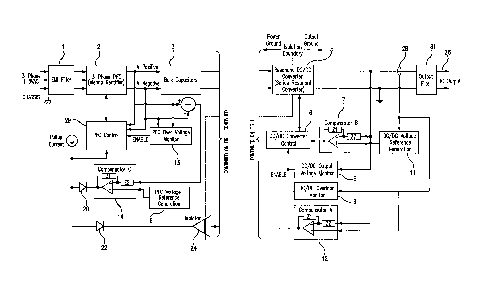
[00016] FIG. 1 is a system block diagram showing an exemplary embodiment
of the
improved R-TRU disclosed herein.
[00017] FIG. 2a is a top level circuit diagram showing features of a
Vienna
Rectifier that may be used in the FIG. 1 embodiment.
[00018] FIG. 2b is a top level circuit diagram showing the features of a
series
resonant DC to DC converter that may be used in the FIG. 1 embodiment to
provide a
270 V DC output.
[00019] FIG. 2c is a top level circuit diagram showing the features of a
series
resonant DC to DC converter that may be used in the FIG. I embodiment to
provide a
28 V DC output, and which uses switching FETs instead of diodes to generate
the DC
output.
DETAILED DESCRIPTION OF AN EXEMPLARY EMBODIMENT
[00020] An exemplary embodiment is described herein with reference to
the system
block diagram depicted in FIG. 1. As used herein and in the claim language,
terms
such as "coupled to" or "connected to" shall be broadly interpreted to mean
elements
that are coupled or connected to other elements either directly or through
intervening
elements. The more restrictive term "couple directly to" or "connected
directly to" will
be used to describe couplings or connections that exclude intervening
elements.
[00021] Referring to FIG. I, unregulated three-phase AC power from, for
example,
an aircraft's generators, is first connected to an EMI (electromagnetic
interference)
filter 1. As mentioned above, the frequency of the input voltage may vary over
a wide
range (e.g., 300-800 Hz). EMI filter 1 attenuates RF voltage/currents at the
three-phase
power input and prevents them from propagating both downstream as well as
upstream.
4
CA 03027151 2018-12-07
WO 2017/223065
PCT/US2017/038293
[00022] In the exemplary embodiment of FIG.1, the EMI-filtered voltage
at the
output of EMI filter 1, is coupled to a three phase Vienna Rectifier 2. Vienna
Rectifier
2 is a known rectifier topology that incorporates power factor control (PFC)
circuitry to
increase the power factor of the rectifier as closely as possible to unity.
This increases
overall system efficiency by reducing power dissipation caused by mismatch of
voltage/current phases at the power input of the rectifier. Power factor
control in a
Vienna Rectifier is accomplished by actively controlling the input side of the
rectifier to
draw sinusoidal current from the three phase power input, thereby providing
near unity
power factor. The DC output of the Vienna Rectifier 2 may typically be
controlled in
the range of +/- 190 VDC to +/- 400 VDC, depending on the input AC voltage
range.
FIG. 2a shows a top level schematic of a Vienna Rectifier topology in which
the power
factor is actively controlled by FET switches.
[00023] While a Vienna Rectifier 2 is used in the FIG. 1 embodiment,
other
rectifiers that include PFC circuits to control and increase the power factor
between
input and output may be used, e.g., a three phase six-switch PFC Rectifier
well known
in the art, or other lesser known PFC rectifier topologies.
[00024] As shown, the Vienna Rectifier 2 in the exemplary embodiment of
FIG. 1
produces a high voltage rail at its output that may nominally be +1- 200 VDC.
As
shown in FIG.1, this DC output is coupled to one or more bulk capacitors in
circuit
block 3 to reduce ripple currents from entering the next stage and to
stabilize the DC
bus. Such ripple currents are produced by the Vienna Rectifier front end and
also may
include line frequency ripple. Because of the three phase AC input, the value
of the
capacitor(s) may be significantly lower than for a single phase AC input.
Common
capacitance values may be in the range of 100 microfarads to 500 microfarads
for
multi-kilowatt converters.
[00025] In FIG. 1, the filtered output from block 3 is connected to a
Resonant DC-
DC converter 5. The Resonant DC/DC Converter 5 converts the high voltage DC on
its
input to a galvanically isolated, lower voltage DC on its output.
5
CA 03027151 2018-12-07
WO 2017/223065
PCT/US2017/038293
[00026] For aircraft applications, the DC output voltage may typically
be +28V DC,
+/-135V DC, or +270V DC. The Resonant DC/DC Converter 5 has limited regulation
capability, per se. The Resonant DC/DC Converter voltage gain may be in the
range of
OVN to Ns/Np VN, where Ns is the number of secondary turns in the DC/DC
transformer and Np is the number of primary turns in the DC/DC transformer.
[00027] In operation, the voltage gain of the Resonant DC/DC Converter 5
is
purposely limited in order to provide maximum efficiency and to prevent it
from being
capable of causing an over-voltage condition in the case of a failure.
[00028] In the exemplary FIG. 1 embodiment, the Resonant DC/DC
Converter 5 is
a phase shift-modulated, full-bridge series resonant DC-DC converter driven at
or near
its resonant frequency (e.g., 120 kHz). The key components of this topology
are
illustrated in FIGS. 2b and 2c.
[00029] There are numerous advantages gained by using this type of DC/DC
Converter architecture in an R-TRU. First, by using a phase shift modulated
full-
bridge series resonant converter (SRC), one has the ability to very precisely
limit the
output voltage rise time as well as the inrush current demanded by load
equipment,
providing good "soft start" characteristics.
[00030] Other topologies, such as a frequency modulated LLC converter
known in
the art, do not provide good control of output voltage rise and output current
during soft
start. For example, if a highly capacitive load were to be connected to the
output of
other converter designs, e.g., a frequency-modulated LLC converter, the
resulting large
in-rush current may produce excessive cun-ent stress in its switching power
FETs, as
well as voltage stress on the resonant capacitor, making a full-bridge series
resonant
converter better suited for the power distribution systems described herein.
[00031] Other topologies, such as a frequency-modulated, half-bridge LLC
converter, are also not capable of precisely regulating the output current
during a short
circuit. If a short circuit occurs on the output, the switching frequency may
be increased
within the capabilities of the power FETs, but the output current can still
reach levels
6
CA 03027151 2018-12-07
WO 2017/223065
PCT/US2017/038293
high enough to create significant, and potentially damaging current stress in
the power
FETs and voltage stress on the resonant capacitor.
[00032] Further, for power distribution equipment, such as an R-TRU, the
output
must regulate elevated short circuit current into a faulted load long enough
to trip a
circuit breaker, which may take up to 5 seconds, or longer, to occur. This
makes other
converter topologies, such as a half-bridge LLC converter, unsuitable for such
power
distribution applications.
[00033] On the other hand, a phase shift-modulated full bridge SRC
topology, as
used herein, permits precise regulation of current during overload conditions
to prevent
damage to the R-TRU electronics, but still trip individual breakers within the
power
distribution network so that the other load equipment may continue to operate.
[00034] Still further, other topologies, depending on loading conditions,
may
produce very high output voltages if the control is faulted. This
characteristic of, for
example, a half-bridge LLC resonant converter, makes it possible for such
other
topologies to create a damaging failure condition, which could create a
hazardous
condition due to excessively high voltage on the aircraft power distribution
bus. On the
other hand, the series resonant converter topology used herein is not capable
of creating
an elevated output voltage, but rather can only reduce the output voltage in
the event of
a fault condition.
[00035] Yet another advantage of using a series resonant converter is
reduced
switching losses, since such resonant converters are able to switch at zero-
current and
zero-voltage conditions.
[00036] It should be noted however, that while a phase shift-modulated
full bridge
series resonant DC-DC converter having the foregoing advantages is used in the
exemplary embodiment of FIG. 1, other DC/DC converters having different
topologies
may also be used without departing from the spirit of the invention, as
described by all
of the disclosed features.
7
[00037] As shown in FIG. 1, the output of the Resonant DC/DC Converter
5 is
coupled to an Output Filter 81, which filters the Converter's output to reduce
voltage
ripple at DC Output 26 and to aid in providing EMI/EMC compliance.
[00038] FIG. 2b shows an example of the basic topology of the Resonant
DC/DC
Converter 5 that may be used in the exemplary FIG.1 embodiment. As shown
therein,
four power FETs 20, 30, 40, 50 on the input side of FIG. 2b are used to drive
a
transformer 60 at high frequency. The transformer 60 is in series with a
capacitor C 62
and inductor L 61. The power FETs 20, 30, 40, 50 are switched at or near the
resonant
frequency fr of this tank circuit (fr= ), e.g., at 120
kHz. At the output side of the
transformer 60, the high frequency AC voltage is rectified by four diodes 70,
80, 90,
100, as shown in FIG. 2b to produce a 270V DC output.
[00039] FIG. 2c shows a slightly different embodiment of a series
resonant DC to
DC converter for producing a DC output, e.g., of 28 V DC. In FIG. 2c, like
components to those in FIG. 2b are shown with the same reference numerals.
[00040] A further advantage of using a series resonant DC-DC Converter
is that this
topology is inherently limited in gain. It cannot create a higher voltage
output than
determined by the turns ratio Ns/Np of the transformer and its input DC
voltage.
However, it can be easily regulated to reduce its output voltage to a desired
value by
controlling the duty cycle of the switching power FETs.
[00041] This is in contrast to prior art system that may use a half-
bridge LLC
converter in a non-regulating mode, without any feedback loop to control the
DC/DC
converter output voltage. In such prior art, the output voltage may be
controlled open
loop, by first starting the DC/DC converter at a high frequency, and then
reducing the
frequency down to the resonant frequency. While this may allow rough soft
start, it
does not provide a system that can tightly regulate the output voltage or
current.
[00042] As further detailed herein, in the FIG.1 exemplary embodiment
of the
invention, three different feedback loops are provided to ensure that the DC
output
8
CA 3027151 2020-01-15
CA 03027151 2018-12-07
WO 2017/223065
PCT/US2017/038293
cannot rise to a damaging level that may endanger the safety of the aircraft.
Referring
to FIG. 1. Compensator A circuit 12 is part of a first feedback loop that
nominally
regulates the output voltage of the R-TRU unit by controlling the output
voltage of the
three phase Vienna Rectifier 2. As shown, it samples the output voltage of the
DC/DC
Converter 5 at its inputs and is coupled to Vienna Rectifier 2 through PFC
Control 29.
[00043] As also shown in FIG. 1, Compensator B circuit 7 is part of a
second
feedback loop that operates to reduce the output voltage of the DC/DC Resonant
Converter 5, if necessary. It is coupled to control the DC/DC Resonant
Converter 5
through DC/DC Converter Control 6 based on measuring the output of the DC/DC
Resonant Converter 5. Finally, Compensator C circuit 14 is part of a third
feedback
loop that effectively controls the output voltage of the Vienna Rectifier 2 by
being
coupled to PFC Control 29, which is in turn directly coupled to control the
Vienna
Rectifier 2.
[00044] This three feedback loop architecture prevents the output
voltage from
rising too high under various fault scenarios and offers fault tolerance to
prevent
damaging over-voltage conditions from appearing on the DC output.
[00045] As described further herein, the Compensator A circuit 12 nominally
regulates the output voltage of the Vienna Rectifier 2 during nofinal
operating
conditions. As a consequence, Compensator B circuit 7 is not required to
regulate the
output of the Resonant DC/DC converter 5 for the majority of the time. This
allows the
Resonant DC/DC Converter 5 to operate in a fully on state. In this
configuration. it will
provide the highest power conversion efficiency and can be optimized for small
size. A
highly optimized series resonant converter operates at, or very near, the
resonant tank
frequency so that all power FETs are operated in a soft switching mode.
[00046] Reverting to FIG. 1, DC/DC Converter Control 6 generates the
driving
waveforms for switching the power FETs in the Resonant DC/DC Converter 5. As
discussed further below, in the FIG.1 embodiment this regulation is achieved
by the
compensator B circuit 7 which is directly coupled to control the DC/DC
Converter
Control 6. Compensator B Circuit 7 is part of a feedback loop that controls
the DC/DC
9
CA 03027151 2018-12-07
WO 2017/223065
PCT/US2017/038293
Converter Control 6 to reduce the output voltage of the Resonant DC/DC
Converter 5
by varying the duty cycle of the FETs in the Resonant DC/DC Converter 5. This
permits desired regulation of the DC output voltage, while not allowing a
deleterious
DC over-voltage to be generated.
[00047] As mentioned above, during normal operation, the Compensator B
circuit 7
operates in a saturated mode. However, the Compensator B circuit 7 will
provide
output voltage and output current control of the Resonant DC/DC Converter 5
for
purposes of soft start and when fault conditions occur as a result of input
voltage
transients, output overload and output short circuit.
[00048] In particular, as shown in FIG. 1, Compensator B circuit 7
samples the
output voltage of the Resonant DC/DC Converter 5 at its inputs. If Compensator
B
circuit 7 senses that this output voltage starts to go too high, then it sends
the
appropriate signals to DC/DC Converter Control 6 to reduce the voltage output
from
the Resonant DC/DC Converter 5 by reducing the duty cycle of the switching
FETs
(e.g., FETs 20, 30, 40, 50 of FIG. 2b) on the input side of the Resonant DC/DC
Converter 5.
[00049] In an exemplary embodiment, such duty cycle control may be achieved
by
modulating the relative phase between the signals driving the switching FETs,
which in
turn will change the duty cycle of the voltage applied to the transformer 60
within the
Resonant DC/DC Converter 5. The feedback loop including Compensator B circuit
7
thus acts to prevent a dangerous over-voltage condition at the DC output 26.
[00050] As further shown in FIG.1, a DC/DC Output Voltage Monitor 8 may
be
optionally provided to monitor the DC output voltage of the Resonant DC/DC
Converter 5 and provide a shut-down signal to DC/DC Converter Control 6 that
turns
off the Resonant DC/DC Converter 5 in the event of an over-voltage fault.
[00051] Additionally, a DC/DC Overload Monitor 9 may also be optionally
provided that detects the output current being provided to an external load.
If the
output load current exceeds a maximum value, the DC/DC Overload Monitor 9 will
CA 03027151 2018-12-07
WO 2017/223065
PCT/US2017/038293
send a signal to the DC/DC Converter Control 6 to shut down and protect the
Resonant
DC/DC Converter 5 from excessive current draw that may damage its circuitry in
the
event of an overload or short circuit.
[00052] Additional features shown in the exemplary FIG. 1 embodiment
include
circuit 11, which generates a reference voltage for use in controlling the
DC/DC
Resonant Converter 5. As shown in FIG. 1, the DC/DC Voltage Reference
Generation
circuit 11 provides a reference voltage (e.g., 2.5 V) to Compensator B circuit
7 and to
the main feedback loop voltage Compensator A circuit 12. The reference voltage
is
also used to provide a "soft start" condition for the DC/DC Resonant Converter
5.
During start up, the DC/DC Voltage Reference Generation circuit 11 causes the
reference voltage to ramp up at a controlled rate to reduce excessive in-rush
currents
and stresses on its power devices that would otherwise occur during the
startup phase.
For example, the reference voltage may initially be at a low level and will
ramp up
gradually to, e.g., 2.5 volts, to provide a corresponding gradual turn-on of
the Resonant
DC/DC Converter 5.
[00053] As shown in FIG. 1, the DC/DC Voltage Reference Generation
circuit 11
may also be connected to a current sensor 28 to sense an overload current
condition.
Should this occur, the reference voltage will be reduced to cause the output
voltage of
the Resonant DC/DC Converter 5 to be "fold backed" to a lower voltage to
protect the
Resonant DC/DC Converter 5 and prevent damage from an overload condition.
[00054] Referring again to FIG. 1, the PFC Control circuit 29 provides
switching
waveforms that control the power FETs in the 3-phase Vienna Rectifier 2. A PFC
Over-voltage Monitor 13 may be optionally provided to monitor the output
voltage of
the Vienna Rectifier 2 and cause the PFC Control circuit 29 to shut down the
Vienna
Rectifier 2 if an over-voltage condition occurs.
[00055] Significantly, the FIG. 1 exemplary embodiment includes two
additional
feedback control loops to control the output voltage and prevent an over
voltage
condition from doing damage. Specifically, Compensator A circuit 12 and
11
CA 03027151 2018-12-07
WO 2017/223065
PCT/US2017/038293
Compensator C circuit 14 are each provided in feedback loops that provide
feedback to
the Vienna Rectifier 2.
[00056] Compensator A circuit 12 is the primary feedback loop that
regulates the
DC output voltage of the Vienna Rectifier 2. As shown in FIG. 1, Compensator A
circuit 12 measures the output voltage of the Resonant DC/DC Converter 5, and
is
arranged as shown to control PFC Control circuit 29 and, in turn, the Vienna
Rectifier 2
in the event of an anomalous fault condition, as further discussed below.
Since the
Resonant DC/DC converter 5 has a maximum voltage gain dictated by the turns
ratio of
its transformer, the DC/DC Converter Control 6 normally will not regulate the
output
voltage.
[00057] The Compensator C circuit 14 also provides feedback control over
the
output of the Vienna Rectifier 2 under appropriate conditions. In practice,
the voltage
regulation point for this Compensator C is set slightly higher than what is
required to
regulate the DC output. Thus, under normal conditions, it will not regulate
the output
of the Vienna Rectifier 2. However, Compensator C circuit 14 will be active
during
failure of the other feedback loops or during startup to regulate the output
voltage to
Vienna Rectifier 2.
[00058] With further reference to FIG. 1, PFC Voltage Reference
Generation circuit
16 provides a reference voltage to the Compensator C circuit 14. This is
typically a
static voltage, but it slowly rises from OV to the reference potential during
startup to
provide soft start of the Vienna Rectifier 2.
[00059] In the FIG. 1 embodiment, as discussed below, whichever one of
Compensators A or C has a lower output voltage will be able to control PFC
Control
circuit 29, and hence the Vienna Rectifier 2. In this regard, under normal
circumstances, the Resonant DC/DC Converter 5 is running at its full output,
which
results in the highest efficiency conversion.
[00060] In particular, as shown in FIG. 1, a pull-up current is injected
at point 18.
This pull up current, in combination with diodes 20 and 22, permits whichever
of the
12
CA 03027151 2018-12-07
WO 2017/223065
PCT/US2017/038293
two Compensators A or C has the lowest output voltage to control the PFC
Control
circuit 29. For example, if one of these compensators, e.g., Compensator C
circuit 14,
tries to overdrive the Vienna Rectifier 2, by providing a higher voltage to
PFC Control
circuit 29, then diode 20 at its output, will become reverse biased and
prevent the
output of the Compensator C circuit 14 from reaching the PFC Control circuit
29. In
that event, the Compensator A circuit 12 will be controlling the PFC Control
block 29.
Likewise, if Compensator A circuit 12 tries to overdrive the Vienna Rectifier
2, its
output will reverse bias its corresponding diode 22 and in that event, the
Compensator
C circuit 14 will control the PFC Control circuit 29.
[00061] In addition, the exemplary embodiment of FIG. 1 provides
galvanic
isolation between input and output. Specifically, such galvanic isolation is
provided by
the transformer 60 in Resonant DC/DC Converter 5, and by an opto-isolator in
isolation
amplifier 24.
[00062] Further, in the exemplary embodiment of FIG. 1, even if the
Compensator
A circuit 12 and the Compensator C circuit 14 both failed, causing an increase
in the
output voltage of the Vienna Rectifier 2 and a corresponding rise in the DC
output of
the Resonant DC/DC Converter 5, the Compensator B circuit 7 will automatically
reduce the output voltage of the Resonant DC/DC Converter 5 to avoid damage
that
may be caused by an over-voltage appearing at the DC Output 26.
[00063] Further, and as noted above, should Compensator B circuit 7
fail, thereby
causing the DC/DC Converter Control 6 to push for more voltage at the output
of the
Resonant DC/DC Converter 5, the turns ratio of its resonant transformer will
inherently
prevent this from happening.
[00064] As disclosed herein, multiple levels of protection are built
into the FIG.1
embodiment to prevent an over-voltage from appearing at the DC output 26,
based on
the feedback control of the Vienna Rectifier 2 provided by Compensator A
circuit 12
and Compensator C circuit 14; the feedback control of the Resonant DC/DC
Converter
5 provided by Compensator B circuit 7, and the inherent over-voltage
protection
provided by the turns ratio of the transformer 60 in the Resonant DC/DC
Converter 5.
13
CA 03027151 2018-12-07
WO 2017/223065 PCT/US2017/038293
[000651 The Table below shows various potential fault scenarios that may
occur in
the disclosed system by describing potential single and double fault
conditions and the
resulting outcome (mitigation). As summarized by this Table, the disclosed
embodiment provides over-voltage protection for up to two simultaneous
failures
without the need for any monitoring circuitry. If an optional DC/DC Output
Voltage
Monitor 8 and optional PFC Over Voltage Monitor 13 are added (see, FIG. 1)
this will
increase the number of required failures to three or four before a damaging
over-voltage
condition could occur. This makes the likelihood of a damaging over-voltage
failure
extremely low.
Scenario Failure #1 Failure #2 Mitigation
Number
1 Compensator A Compensator C takes
faults and control of the Vienna
attempts to cause Rectifier and
an over voltage of prevents an output
the Vienna over voltage.
Rectifier output.
2 Compensator C Compensator A takes
faults and control of the Vienna
attempts to cause Rectifier and
an over voltage of prevents an output
the Vienna over voltage.
Rectifier output.
3 Compensator B Compensator A takes
faults and control of the Vienna
attempts to cause Rectifier and
an over voltage of prevents an output
the Resonant over voltage. Also,
DC/DC Converter Compensator B can
output. only reduce the
output voltage of the
Resonant DC/DC
Converter, and
cannot increase the
DC output voltage to
a damaging level.
4 Compensator A Compensator C Compensator B
faults and faults and attempts controls the
Resonant
attempts to cause to cause an over DC/DC converter to
an over voltage of voltage of the reduce the output
14
CA 03027151 2018-12-07
WO 2017/223065 PCT/US2017/038293
the Vienna Vienna Rectifier voltage and prevent
Rectifier output. output. an over voltage.
Compensator A Compensator B Compensator B
faults and faults and attempts cannot increase the
attempts to cause to cause an over output voltage of the
an over voltage of voltage of the Resonant DC/DC
the Vienna Resonant DC/DC converter since a
Rectifier output. Converter output. series resonant
converter cannot
increase its output
voltage above the
transformer turns
ratio times the input
voltage. The output
voltage can only be
reduced.
In this scenario,
Compensator C takes
control of the Vienna
Rectifier output
voltage and prevents
an over voltage on
the output.
6 Compensator B Compensator C Compensator A takes
faults and faults and attempts control of the
Vienna
attempts to cause to cause an over Rectifier and
an over voltage of voltage of the prevents an output
the Resonant Vienna Rectifier over voltage.
DC/DC Converter output.
output.
[00066] Although the disclosed subject matter has been described and
illustrated
with respect to the exemplary embodiments provided herein, it will be
understood by
those of ordinary skill in the art that various additions and modifications
may be made
5 to these disclosed embodiments without departing from the spirit and
scope of the
innovations disclosed herein, which are set forth in the following claims.
15