Note : Les descriptions sont présentées dans la langue officielle dans laquelle elles ont été soumises.
CA 03029899 2019-01-03
WO 2018/009910 PCT/US2017/041262
IMPLANTS USING ULTRASONIC BACKSCATTER FOR DETECTING
ELECTROPHYSIOLOGICAL SIGNALS
CROSS-REFERENCE TO RELATED APPLICATION
[0001] This application claims priority to U.S. Provisional Application No.
62/359,672, filed
on July 7, 2016, entitled "NEURAL DUST AND ULTRASONIC BACKSCATER IMPLANTS
AND SYSTEMS, AND APPLICATIONS FOR SUCH SYSTEMS," which is incorporated
herein by reference for all purposes.
STATEMENT AS TO FEDERALLY SPONSORED RESEARCH
[0002] This invention was made with government support under Grant Nos.
HR0011-15-2-
0006 awarded by the Defense Advanced Research Projects Agency (DARPA) and R21-
E027570
awarded by the National Institute of Health (NIH).
TECHNICAL FIELD
[0003] The present invention relates to implantable devices for sensing
electrophysiological
voltage signals in tissue, and reporting the same using ultrasonic
backscatter.
BACKGROUND
[0004] The emerging field of bioelectronic medicine seeks methods for
deciphering and
modulating electrophysiological activity in the body to attain therapeutic
effects at target organs.
Current approaches to interfacing with peripheral nerves, the central nervous
system, and
muscles rely heavily on wires, creating problems for chronic use, while
emerging wireless
approaches lack the size scalability necessary to interrogate small-diameter
nerves. Furthermore,
conventional electrode-based technologies lack the capability to record from
nerves with high
spatial resolution or to record independently from many discrete sites within
a nerve bundle.
[0005] Recent technological advances and fundamental discoveries have
renewed interest in
implantable systems for interfacing with the peripheral nervous system. Early
clinical successes
with peripheral neurostimulation devices, such as those used to treat sleep
apnea or control
bladder function in paraplegics have led clinicians and researchers to propose
new disease targets
ranging from diabetes to rheumatoid arthritis.
1
CA 03029899 2019-01-03
WO 2018/009910 PCT/US2017/041262
[0006] There remains a need for new electrode-based recording technologies
that can detect
abnormalities in physiological signals and be used to update stimulation
parameters in real time.
Features of such technologies preferably include high-density, stable
recordings of a large
number of channels in single nerves, wireless and implantable modules to
enable
characterization of functionally specific neural and electromyographic
signals, and scalable
device platforms that can interface with small nerves of 100 mm diameter or
less, as well as
specific muscle fibers. Current approaches to recording peripheral nerve
activity fall short of
this goal; for example, cuff electrodes provide stable chronic performance but
are limited to
recording compound activity from the entire nerve. Single-lead intrafascicular
electrodes can
record from multiple sites within a single fascicle but do not enable high-
density recording from
discrete sites in multiple fascicles. Similarly, surface EMG arrays allow for
very-high-density
recording but do not capture fine details of deep or small muscles. Recently,
wireless devices to
enable untethered recording in rodents and nonhuman primates, as well as mm-
scale integrated
circuits for neurosensing applications have been developed. See, e.g.,
Biederman et al., A 4.78
mm2 fully-integrated neuromodulation SoC combining 64 acquisition channels
with digital
compression and simultaneous dual stimulation, IEEE J. Solid State Circuits,
vol. 5, pp. 1038-
1047 (2015); Denison et al., A 2,uW 100 nV/rtHz chpper-stabilized
instrumentation amplifier for
chronic measurement of neural field potentials, IEEE J. Solid State Circuits,
vol. 42, pp. 2934-
2945 (2007); and Muller et al., A minimially invasive 64-channel wireless
uECOoG implant, IEE
J. Soid State Circuits, vol. 50, pp. 344-359 (2015). However, most wireless
systems use
electromagnetic (EM) energy coupling and communication, which becomes
extremely inefficient
in systems smaller than ¨5 mm due to the inefficiency of coupling radio waves
at these scales
within tissue. Further miniaturization of wireless electronics platforms that
can effectively
interface with small-diameter nerves will require new approaches.
SUMMARY OF THE INVENTION
[0007] Provided herein is an implantable device configured to detect an
electrophysiological
signal, and methods of detecting an electrophysiological signal, in tissue
(such as muscle or
nervous tissue). Also provided herein are systems including one or more
implantable devices
and an interrogator for operating the one or more implantable devices.
2
CA 03029899 2019-01-03
WO 2018/009910 PCT/US2017/041262
[0008] In some embodiments, an implantable device comprises a first
electrode and a second
electrode configured to engage a tissue and detect an electrophysiological
signal; an integrated
circuit comprising a multi-transistor circuit and a modulation circuit
configured to modulate a
current based on the electrophysiological signal; and an ultrasonic transducer
configured to emit
an ultrasonic backscatter encoding the electrophysiological signal from the
tissue based on the
modulated current.
[0009] In some embodiments, the multi-transistor circuit is a digital
circuit. In some
embodiments, the digital circuit is configured to operate the modulation
circuit. In some
embodiments, the digital circuit is configured to transmit a digitized signal
to the modulation
circuit, wherein the digitized signal is based on the detected
electrophysiological signal. In some
embodiments, the digitized signal comprises a unique implantable device
identifier or a unique
electrode pair identifier. In some embodiments, the digitized signal is
compressed by a factor of
or more relative to an analog signal.
[0010] In some embodiments, the implantable device comprises a body that
comprises the
ultrasonic transducer and the modulation circuit, wherein the body is about 5
mm or less in
length in the longest dimension. In some embodiments, the first electrode and
the second
electrode are spaced by about 0.5 mm or more. In some embodiments, the
implantable device
comprises a body that comprises the ultrasonic transducer and the modulation
circuit, wherein
the body of the implantable device has a volume of about 5 mm3 or less.
[0011] In some embodiments, the implantable device comprises a non-
responsive reflector.
[0012] In some embodiments, the tissue is muscular tissue or nervous
tissue. In some
embodiments, the tissue is part of the peripheral nervous system or the
central nervous system.
In some embodiments, the tissue is brain tissue or a peripheral nerve. In some
embodiments, the
tissue is skeletal muscle, cardiac muscle, or smooth muscle.
[0013] In some embodiments, the implantable device comprises three or more
electrodes. In
some embodiments, the integrated circuit comprises a spike detector. In some
embodiments, the
integrated circuit comprises a power circuit. In some embodiments, the
integrated circuit
comprises an analog-to-digital converter (ADC),In some embodiments, the
integrated circuit
comprises an amplifier chain.
[0014] In some embodiments, the ultrasonic transducer is configured to
receive ultrasonic
waves that power the implantable device. In some embodiments, the ultrasonic
transducer is
3
CA 03029899 2019-01-03
WO 2018/009910 PCT/US2017/041262
configured to receive ultrasonic waves from an inten-ogator comprising one or
more ultrasonic
transducers. In some embodiments, the ultrasonic transducer is a bulk
piezoelectric transducer, a
piezoelectric micro-machined ultrasonic transducer (PMUT), or a capacitive
micro-machined
ultrasonic transducer (CMUT).
[0015] In some embodiments, the implantable device is implanted in a
subject. In some
embodiments, the subject is a human. In some embodiments, the implantable
device is implanted
in the tissue, on the tissue, or near the tissue. In some embodiments, the
first electrode and the
second electrode are implanted in the tissue or on the tissue.
[0016] In some embodiments, he implanted device is at least partially
encapsulated by a
biocompatible material. In some embodiments, at least a portion of the first
electrode and the
second electrode are not encapsulated by the biocompatible material.
[0017] Also provided herein is a system comprising one or more implantable
devices and an
interrogator comprising one or more ultrasonic transducers configured to
transit ultrasonic waves
to the one or more implantable devices or receive ultrasonic backscatter from
the one or more
implantable devices. In some embodiments, the system comprises a plurality of
implantable
devices. In some embodiments, the interrogator is configured to beam steer
transmitted
ultrasonic waves to alternatively focus the transmitted ultrasonic waves on a
first portion of the
plurality of implantable devices or focus the transmitted ultrasonic waves on
a second portion of
the plurality of implantable devices. In some embodiments, the interrogator is
configured to
simultaneously receive ultrasonic backscatter from at least two implantable
devices. In some
embodiments, the interrogator is configured to transit ultrasonic waves to the
plurality of
implantable devices or receive ultrasonic backscatter from the plurality of
implantable devices
using time division multiplexing, spatial multiplexing, or frequency
multiplexing. In some
embodiments, the interrogator is configured to be wearable by a subject.
[0018] Further provided herein is a computer system, comprising: an
interrogator comprising
one or more ultrasonic transducers; one or more processors; non-transitory
computer-readable
storage medium storing one or more programs configured to be executed by the
one or more
processors, the one or more programs comprising instructions for detecting an
electrophysiological signal based on ultrasonic backscatter encoding the
electrophysiological
pulse emitted from an implantable device; and determining a location of the
implantable device
relative to the one or more ultrasonic transducers of the interrogator, or
detecting movement of
4
CA 03029899 2019-01-03
WO 2018/009910 PCT/US2017/041262
the implantable device, based on ultrasonic backscatter not responsive to the
electrophysiological
pulse emitted from the implantable device. In some embodiments, the one or
more programs
comprise instructions for determining a location or movement of the
implantable device relative
to the one or more ultrasonic transducers of the interrogator. In some
embodiments, the
ultrasonic backscatter responsive to the electrophysiological signal comprises
a digitized signal
encoding the electrophysiological signal. In some embodiments, the one or more
programs
comprises instructions for attributing the detected electrophysiological
signal to the implantable
device that emitted the ultrasonic backscatter encoding the
electrophysiological signal from a
plurality of implantable devices. In some embodiments, the detected
electrophysiological signal
is attributed to the implantable device using time division multiplexing,
spatial multiplexing, or
frequency multiplexing. In some embodiments, the detected electrophysiological
signal is
attributed to the implantable device using a unique identifier encoded in the
ultrasonic
backscatter encoding the electrophysiological pulse.
[0019] Also provided herein is a method of detecting an
electrophysiological signal in a
tissue, comprising receiving ultrasonic waves at one or more implantable
devices; converting
energy from the ultrasonic waves into an electrical current that flows through
a modulation
circuit; detecting the electrophysiological signal; digitizing the
electrophysiological signal;
modulating the electrical current based on the digitized electrophysiological
signal; transducing
the modulated electrical current into an ultrasonic backscatter that encodes
information related to
the electrophysiological signal; and emitting the ultrasonic backscatter to an
interrogator
comprising one or more transducer configured to receive the ultrasonic
backscatter.
[0020] In some embodiments, there is a method of detecting an
electrophysiological signal in
a tissue, comprising transmitting ultrasonic waves from an interrogator
comprising one or more
ultrasonic transducers to one or more implantable devices; and receiving from
the one or more
implantable devices ultrasonic backscatter that encodes digitized information
related the
electrophysiological signal.
[0021] In some embodiments, the method comprises receiving the ultrasonic
backscatter
using the interrogator. In some embodiments, the ultrasonic waves power the
one or more
implantable devices.
[0022] In some embodiments of the methods provided herein, the tissue is
muscular tissue or
nervous tissue. In some embodiments, the tissue is part of the peripheral
nervous system or the
CA 03029899 2019-01-03
WO 2018/009910 PCT/US2017/041262
central nervous system. In some embodiments, the tissue is brain tissue or a
peripheral nerve. In
some embodiments, the tissue is skeletal muscle, cardiac muscle, or smooth
muscle.
[0023] In some embodiments, the method comprises reconstructing an
electromyogram, an
electroneurogram, an electrocardiogram, a compound action potential, a multi-
unit activity of
multiple neurons, a local field potential, or an action potential.
[0024] In some embodiments, the method comprises implanting the one or more
implantable
devices. In some embodiments, the subject is a human.
[0025] In some embodiments, the method comprises determining a location or
movement of
the one or more implantable devices.
[0026] In some embodiments of the methods provided herein, the digitized
signal comprises
a unique implantable device identifier or a unique electrode pair identifier.
[0027] In some embodiments of the methods provided herein, the one or more
implantable
devices comprises a plurality of implantable devices.
BRIEF DESCRIPTION OF THE FIGURES
[0028] FIG. 1 is a schematic of a neural dust system, including an external
transceiver, a sub-
dural interrogator, and a neural dust mote, as described in Seo et al., Neural
dust: an ultrasonic,
low power solution for chronic brain-machine interfaces, arXiv: 1307.2196v1
(July 8, 2013).
[0029] FIG. 2A is a block diagram of an exemplary interrogator for a system
described
herein. The illustrated interrogator includes an ultrasonic transducer array
comprising a plurality
of ultrasonic transducers. Each of the ultrasonic transducers in the array is
operated by a
channel, which includes a switch to alternatively configure the transducer to
receive or transmit
ultrasonic waves. FIG. 2B is a schematic of another exemplary interrogator for
a system
described herein. The illustrated interrogator includes two ultrasonic
transducer arrays, with
each ultrasonic transducer array including a plurality of ultrasonic
transducers. The interrogator
also includes an integrated circuit (which can include a digital circuit,
which can include a
processor). The integrated circuit is connected to a user interface (which can
include a display,
keyboard, buttons, etc.), a storage medium (i.e., a non-transitory memory), an
input/output
(which may be wireless, such as a Bluetooth), and a power supply (such as a
battery).
[0030] FIG. 3A shows a block diagram of an exemplary interrogator that can
be worn by a
subject. The interrogator includes a wireless communication system (a
Bluetooth radio, in the
6
CA 03029899 2019-01-03
WO 2018/009910 PCT/US2017/041262
illustration), which can be used to communicate with a computer system. FIG.
3B shows an
exploded view of a wearable interrogator. The intenxigator includes a battery,
a wireless
communication system, and a transducer array. FIG. 3C shows the wearable
interrogator shown
in FIG. 3B fully assembled with a harness for attachment to a subject. FIG. 3D
illustrates the
wearable interrogator attached a subject, namely a rodent (although could be
any other animal,
such as a human, dog, cat, horse, cow, pig, sheep, goat, chicken, monkey, rat
or mouse). The
interrogator includes a transducer array, which is fixed to the body of the
subject by an adhesive.
FIG. 3E illustrates a cross-section of the transducer array of the
interrogator shown in FIGS.
3A-D.
[0031] FIG. 4 provides a schematic showing the communication between a
transducer from
an interrogator and an implantable device having a miniaturized ultrasonic
transducer. The
interrogator transmits ultrasonic waves to the implantable device, and the
miniaturized ultrasonic
transducer emits ultrasonic backscatter modulated by the sensor. The
backscatter is then
received by the interrogator.
[0032] FIG. 5A shows a series of cycles of ultrasonic wave pulses emitted
by an interrogator.
Upon receiving a trigger from the interrogator (e.g., an FPGA), the
transceiver board of the
interrogator generates a series of transmit pulses. At the end of the transmit
cycle, the switch on
the ASIC disconnects the transmit module and connects the receive module. The
cycles have a
frequency of every 100 microseconds. FIG. 5B shows a zoomed-in view of the
transmit pulse
sequence (i.e., one cycle) shown in FIG. 5A, with the cycle having six pulses
of ultrasonic waves
at 1.85 MHz, the pulses recurring every 540 nanoseconds. FIG. 5C shows
ultrasonic backscatter
emitted by an implantable device. The ultrasonic backscatter reaches the
transducer of the
interrogator approximately 2t
-Rayleigh= FIG. 5D shows a zoomed-in view of the ultrasonic
backscatter, which can be analyzed. Analysis of the ultrasonic backscatter can
include filtering,
rectifying and integrating the ultrasonic backscatter waves. FIG. 5E shows a
zoomed in view of
the filtered ultrasonic backscatter waves. The backscatter wave includes
responsive regions,
which are responsive to changes in impedance to the miniaturized ultrasonic
transducer, and non-
responsive regions that are not responsive to changes in impedance to the
miniaturized ultrasonic
transducer.
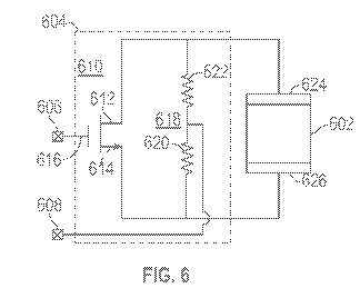
[0033] FIG. 6 illustrates one embodiment of an implantable device having a
miniaturized
ultrasonic transducer, a modulation circuit configured to modulate a current
flowing through the
7
CA 03029899 2019-01-03
WO 2018/009910 PCT/US2017/041262
miniaturized ultrasonic transducer based on an electrophysiological signal
detected by an
electrode pair.
[0034] FIG. 7A illustrates one embodiment of a miniaturized ultrasonic
transducer
(identified as the "piezo") connected to an ASIC. The ASIC includes a power
circuit and a
modulation circuit (or "backscatter circuit"). The power circuit includes an
energy storage
capacitor ("cap"). The electrodes can be implanted in tissue.
[0035] FIG. 7B illustrates an implantable device with a miniaturized
ultrasonic transducer,
and integrated circuit, and a pair of electrodes. The integrated circuit
includes a modulation
circuit, an AC-coupled amplifier chain, and a power circuit, which includes a
full-wave rectifier
and doubler, a reference, and a regulator. FIG. 7C illustrates an exemplary
rectifier that can be
used in the integrated circuit shown in FIG. 7B. FIG. 7D illustrates an
exemplary amplifier
chain that can be used in the integrated circuit shown in FIG. 7B.
[0036] FIG. 8A illustrates a schematic of an exemplary implantable device
including a
miniaturized ultrasonic transducer and an ASIC on a printed circuit board
(PCB). FIG. 8B
illustrates a schematic of another exemplary implantable device including a
miniaturized
ultrasonic transducer and an ASIC on a printed circuit board (PCB).
[0037] FIG. 9 illustrates a method of manufacturing an implantable device
described herein.
[0038] FIG. 10 is a flowchart for a method of encapsulating an implantable
device with
amorphous silicon carbide.
[0039] FIG. 11A shows different geometries of vias used to connect
components of the
implantable device. FIG. 11B shows a serpentine trace configuration for
deformable
interconnects.
[0040] FIG. 12 shows the relationship between time and temperature for
curing silver epoxy,
an exemplary material for attaching wirebonds during the manufacture of the
implantable device.
[0041] FIG. 13 shows a recorded electroneurogram (ENG) using an implantable
device. The
dotted trace shows the signal recorded by the ground truth electrode. A
general profile including
the compound action potentials was reconstructed from the acquired data, which
matches the
profile of the ground truth.
[0042] FIG. 14 illustrates a schematic for encapsulating an implantable
device in silicon
carbide.
[0043] FIG. 15 shows an assembly prototype schematic and PCB.
8
CA 03029899 2019-01-03
WO 2018/009910 PCT/US2017/041262
[0044] FIG. 16A-E show processing steps to ensure that the desired
miniaturized ultrasonic
transducer (PZT) dimension is assembled on the PCB. At FIG. 16A, epoxy solder
paste is
dispensed onto the board. At FIG. 16B, a piezoelectric material is attached to
the PCB. At FIG.
16C, the piezoelectric material is diced to form a bulk piezoelectric
ultrasonic transducer of the
desired size. At FIG. 16D, the ultrasonic transducer is wirebonded to the PCB.
At FIG. 16E, the
PCB and ultrasonic transducer is encapsulated in PDMS.
[0045] FIG. 17 shows a schematic for measuring electrical impedance with a
vector network
analyzer (VNA),
[0046] FIG. 18A shows that the measured power transfer efficiency at
various bulk
piezoelectric ultrasonic transducer sizes matches simulated behavior. FIG. 18B
shows that the
measured impedance spectroscopy of a PZT crystal matches a simulation. FIG.
18C shows that
the frequency response of harvested power of the miniaturized ultrasonic
transducer is
approximately 6.1 MHz.
[0047] FIG. 19 is a schematic of an exemplary ultrasonic transducer that
can be used as part
of an interrogator.
[0048] FIG. 20 is a schematic of a setup for acoustic characterization with
a calibrated
ultrasonic transducer for power delivery verification. The ultrasonic wave
receiver is separate
from the ultrasonic wave transmitter.
[0049] FIG. 21A shows the output power of a 5 MHz transducer as the
hydrophone is moved
away from the transducer's surface. FIG. 21B shows that the de-rated peak is
shifted to the left
in relation to the water peak.
[0050] FIG. 22A shows the XZ cross-section of the transducer output,
illustrating a Rayleigh
distance and a clear transition from the near-field to far-field propagation.
FIG. 22B shows the
XY beam cross-section showing a 6 dB bandwidth of the beam at 2.2 mm.
[0051] FIG. 23A shows a focused 2D beam pattern from a transducer array in
the XY plane.
The measured beam approximates the simulated beam in both the X and Y
dimensions. FIG.
23B shows the delay time applied to each transducer element in the ultrasonic
transducer array.
FIG. 23C shows a simulated 2D XZ cross-sectional beam pattern.
[0052] FIG. 24A shows beam steering of an ultrasonic wave beam transmitted
from a
transducer array. Underneath each beam pattern is the delay for each
transducer in the array to
obtain the measured beam pattern, as shown in FIG. 24B. FIG. 24C shows the 1D
beam pattern
9
CA 03029899 2019-01-03
WO 2018/009910 PCT/US2017/041262
in the X-axis for each beam pattern shown in FIG. 24A. The measured beam
pattern closely
approximates the simulated beam pattern.
[0053] FIG. 25 shows a simulated scaling of miniaturized ultrasonic
transducer link
efficiency and received power at 5 mm in tissue.
[0054] FIGS. 26A-D provide an overview of an exemplary system comprising an
implantable device. FIG. 26A shows an external transducer powering and
communicating an
implantable device placed remotely in the body. Driven by a custom transceiver
board, the
transducer alternates between transmitting a series of pulses that power the
device and listening
for reflected pulses that are modulated by electrophysiological signals. FIG.
26B shows an
implantable device anchored to the sciatic nerve in an anesthetized rat. The
insert in FIG. 26B
shows an implantable device with optional testing leads. FIG. 26C shows
components of an
exemplary implantable device. The implantable device was assembled on a
flexible PCB and
included a piezoelectric crystal, a single custom transistor, and a pair of
recording electrodes.
FIG. 26D shows a close up of an implantable device on a flexible PCG with
calibration leads to
measure electrophysiological signal (ground truth) and voltages harvested on
the piezocrystal.
During in-vivo experiments, the calibration leads were removed.
[0055] FIG. 27 illustrates communication between an exemplary interrogator
and an
implantable device. The top of FIG. 27 is a schematic of the flow of
information. The bottom of
FIG. 27 represents time traces of signals at each step referenced in the
diagram shown at the top
of the figure. At FIG. 27A, the FPGA from the interrogator generates a trigger
signal to initiate
recording. FIG. 27B shows an extracellular, electrophysiological potential
presented to the
recording electrodes on an implantable device. FIG. 27C shows that upon
receiving the trigger
from the FPGA, the transceiver board generates a series of transmit pulses. At
the end of the
transmit cycle, the switch on the ASIC of the interrogator disconnects the
transmit module and
connects the receive module. FIG. 27D shows zoomed-in transmit pulse sequence,
showing 6
pulses at 1.85 MHz. FIG. 27E shows backscatter from the implantable device,
which reaches the
transducer at approximately 2t
_Rayieigh= FIG. 27F shows zoomed-in backscatter waveforms. The
backscatter waveform includes a large saturating signal which overlaps with
the transmitted
pulses is electrical feedthrough and is ignored. When returning, backscattered
pulses can be seen
subsequent to the transmission window. FIG. 27G shows the backscattered
waveforms being
filtered, rectified, and the area under the curve is computed in or der to
produce reconstructed
CA 03029899 2019-01-03
WO 2018/009910 PCT/US2017/041262
waveforms. FIG. 27H shows the reconstructed waveform sampled at 10 kHz. Each
point of the
reconstructed waveform is computed by calculating the area under the curve of
the appropriate
reflected pulses, received every 100 ps.
[0056] FIG. 28A shows the de-rated, normalized peak pressure as a function
of distance from
the surface of an exemplary transducer (interrogator) showed has a de-rated
focus at ¨8.9 mm at
1.85 MHz. FIG. 28B shows the XY cross-sectional beam pattern and the
corresponding 1-D
voltage plot at y = 0 at near-field, Rayleigh distance, and far-field. The
pattern shows the beam
focusing at the Rayleigh distance. FIG. 28C shows that the transducer's output
pressure was a
linear function of input voltage (up to 32 V peak-to-peak). FIG 28D
(reproduction of FIG. 5E)
shows exemplary backscatter waveform showing different regions of backscatter.
The
backscatter waveform is found flanked (in time) by regions which correspond to
reflections
arising from non-responsive regions; these correspond to reflected pulses from
other device
components. The measurement from the nonresponsive regions, which do not
encode biological
data) can be used as a reference. As a result of taking this differential
measurement, any
movements of the entire structure relative to the external transducer during
the experiment can be
subtracted out. FIG. 28E shows a calibration curve obtained in the custom
water tank setup
showed the noise floor of 0.18 mVrms. FIG 28F shows the effect of noise floor
as a function of
lateral misalignment followed the beampattern power fall-off. FIG. 28G shows a
1-D plot of the
transducer's off-axis voltage and power drop-off at y = 0 at Rayleigh
distance. FIG. 28H shows
a plot of the drop in the effective noise floor as a function of angular
misalignment. Angular
misalignment results in a skewed beam pattern: ellipsoidal as opposed to
circular. This increases
the radius of focal spot (spreading energy out over a larger area); the
distortion of the focal spot
relaxes the constraint on misalignment.
[0057] FIG. 29A shows a in-vivo experimental setup for EMG recording from
gastrocnemius
muscle in rats. The implantable device was placed on the exposed muscle
surface and the wound
was closed with surgical suture. The external transducer couples ultrasound to
the implantable
device and the wireless data is recorded and displayed on the computer system
(e.g., laptop).
FIG. 29B shows a comparison between ground truth measurement and the
reconstructed EMG
signals over a number of trials. 20 msec samples were recorded and the inter-
stimulus interval
was 6 sec. FIG. 29C shows a power spectral density (PSD) of the recorded EMG
signal, which
showed 4.29e4 pV2/Hz and 3.11e4 pV2/Hz at 107 Hz for ground truth and the
reconstructed
11
CA 03029899 2019-01-03
WO 2018/009910 PCT/US2017/041262
dust data, respectively, and several harmonics due to edges in the waveform.
FIG. 29D shows
the wireless backscatter data recorded at t = 0 mm and t = 30 min matched with
R = 0.901.
[0058] FIG. 30A shows different intensities of EMG signals were recorded in-
vivo with the
electrodes on the PCB with varying stimulation intensities. FIG. 30B shows
similar gradient
EMG responses were recorded wirelessly with the implantable device. FIG. 30C
shows ground
truth and reconstruction of EMG signal from the wireless backscatter data at
response-saturating
stimulation amplitude (100%) matched with R = 0.795 (R = 0.60, 0.64, 0.67,
0.92 for 54%, 69%,
77%, 89%, respectively). In FIG. 30D, a quantitative comparison showed < 0.4
mV match of the
salient feature. In FIG. 30E, EMG peak-to-peak voltage showed an expected
sigmoidal
relationship with the stimulation intensity.
[0059] FIG. 31A shows different intensities of ENG signals that were
recorded in-vivo with
the electrodes on the PCB with varying stimulation intensities. FIG. 31B shows
similar gradient
ENG responses were recorded wirelessly with the mote. FIG. 31C shows ground
truth and
reconstruction of ENG signal from the wireless backscatter data at response-
saturating
stimulation amplitude (100%) matched with R = 0.886 (R = 0.822, 0.821, 0.69,
0.918, 0.87 for
44%, 61%, 72%, 83%, 89%, respectively). In FIG. 31D, quantitative comparison
showed < 0.2
mV match of the salient feature. In FIG. 31E, ENG peak-to-peak voltage showed
an expected
sigmoidal relationship with the stimulation intensity.
[0060] FIG. 32A shows recorded time-domain ENG responses for different
electrode
spacing. FIG. 32B shows peak-to-peak ENG with varying electrode spacing.
[0061] FIG. 33A shows ultrasonic backscatter from an implantable device,
with the
implantable device implanted inn ultrasound coupling gel used to mimic tissue.
The backscatter
includes a transmit feedthrough and ring-down centered at 26 microseconds, and
the
miniaturized ultrasonic transducer backscatter centered around 47
microseconds. FIG. 33B
shows a close-up on the backscatter region from the miniaturized ultrasonic
transducer (the
responsive region), which shows amplitude modulation as a result of a signal
input to the
implantable device.
[0062] FIG. 34 shows digital data corresponding to ASCII characters 'hello
world'
wirelessly ready from the implantable device through pulse amplitude
backscatter modulation
with unipolar encoding.
12
CA 03029899 2019-01-03
WO 2018/009910 PCT/US2017/041262
DETAILED DESCRIPTION OF THE INVENTION
[0063] The implantable device described herein includes a miniaturized
ultrasonic transducer
(such as a miniaturized piezoelectric transducer) and two or more electrodes
configured to detect
an electrophysiological voltage signal (such as an action potential). The
electrophysiological
voltage signal can be detected, for example, in nervous tissue or muscle
tissue. The miniaturized
ultrasonic transducer receives ultrasonic energy from an interrogator (which
may be external or
implanted), which powers the implantable device. The interrogator includes a
transmitter and a
receiver (which may be integrated into a combined transceiver), and the
transmitter and the
receiver may be on the same component or different components. Mechanical
energy from the
ultrasonic waves transmitted by the interrogator vibrates the miniaturized
ultrasonic transducer
on the implantable device, which generates an electrical current. The current
flowing through
the miniaturized ultrasonic transducer is modulated by the electrical
circuitry in the implantable
device based on the detected electrophysiological voltage signal, and the
modulated current
passes through the miniaturized ultrasonic transducer. The miniaturized
ultrasonic transducer
emits an ultrasonic backscatter communicating information indicative of the
detected
electrophysiological voltage signal, which is detected by the receiver
components of the
interrogator.
[0064] A significant advantage of the implantable device is the ability to
detect
electrophysiological voltage signals in deep tissue while being wirelessly
powered, wirelessly
transmit information relating the detected electrophysiological signal to an
interrogator, which
can be external or relay the information to an external component. Thus, the
implantable devices
can remain in a subject for an extended period of time without needing to
charge a battery or
retrieve information stored on the device. These advantages, in turn, allow
the device to be
smaller and less expensive to manufacture. In another advantage, use of
ultrasound allows for
the relative time for data communication to be related to distance, which can
aid in determining
location or movement of the implantable device in real time.
[0065] Electromagnetic (EM) power transfer is not a practical for powering
small
implantable devices due to power attenuation through tissue and the relatively
large apertures
(e.g. antennas or coils) required to capture such energy. See, for example,
Seo et al., Neural
dust: an ultrasonic, low power solution for chronic brain-machine interfaces,
arXiv:
1307.2196v1 (July 8, 2013). Use of EM to supply sufficient power to an
implanted device
13
CA 03029899 2019-01-03
WO 2018/009910 PCT/US2017/041262
would either require a shallow depth of the implant or would require excessive
heating of the
tissue to pass the EM waves through the tissue to reach the implantable
device. In contrast to
EM, ultrasonic power transfer provides low power attenuation in tissue due to
the relatively low
absorption of ultrasonic energy by tissue and the shorter wavelength of the
ultrasonic waves (as
compared to electromagnetic waves). Further, the shorter wavelengths provided
by the
ultrasonic waves provides high spatial resolution at lower frequencies
compared to radio waves.
[0066] Ultrasonic transducers have found application in various disciplines
including
imaging, high intensity focused ultrasound (HIFU), nondestructive testing of
materials,
communication, and power delivery through steel walls, underwater
communications,
transcutaneous power delivery, and energy harvesting. See, e.g., Ishida et
al., Insole Pedometer
with Piezoelectric Energy Harvester and 2 V Organic Circuits, IEEE J. Solid-
State Circuits, vol.
48, no. 1, pp. 255-264 (2013); Wong et al., Advantages of Capacitive
Micromachined
Ultrasonics Transducers (CMUTs) for High Intensity Focused Ultrasound (HIFU),
IEEE
Ultrasonics Symposium, pp. 1313-1316 (2007); Ozeri et al., Ultrasonic
Transcutaneous Energy
Transfer for Powering Implanted Devices, Ultrasonics, vol. 50, no. 6, pp. 556-
566 (2010); and
Richards et al., Efficiency of Energy Conversion for Devices Containing a
Piezoelectric
Component, J. Micromech. Microeng., vol. 14, pp. 717-721 (2004). Unlike
electromagnetics,
using ultrasound as an energy transmission modality never entered into
widespread consumer
application and was often overlooked because the efficiency of
electromagnetics for short
distances and large apertures is superior. However, at the scale of the
implantable devices
discussed herein and in tissue, the low acoustic velocity allows operation at
dramatically lower
frequencies, and the acoustic loss in tissue is generally substantially
smaller than the attenuation
of electromagnetics in tissue.
[0067] The relatively low acoustic velocity of ultrasound results in
substantially reduced
wavelength compared to EM. Thus, for the same transmission distance,
ultrasonic systems are
much more likely to operate in the far-field, and hence obtain larger spatial
coverage than an EM
transmitter. Further, the acoustic loss in tissue is fundamentally smaller
than the attenuation of
electromagnetics in tissue because acoustic transmission relies on compression
and rarefaction of
the tissue rather than time-varying electric/magnetic fields that generate
displacement currents on
the surface of the tissue.
14
CA 03029899 2019-01-03
WO 2018/009910 PCT/US2017/041262
[0068] In some embodiments, a "neural dust" system comprises tiny body-
implantable
devices referred to as neural dust or "motes", an implantable ultrasound
transceiver that
communicates with each of the motes using ultrasound transmissions and
backscatter
transmissions reflected from the motes, and an external transceiver that
communicates wirelessly
with the ultrasound transceiver. See Seo et al., Neural dust: an ultrasonic,
low power solution
for chronic brain-machine interfaces, arXiv: 1307.2196v1 (July 8, 2013) ("Seo
et al., 2013");
Seo et al., Model validation of untethered, ultrasonic neural dust motes for
cortical recording, J.
Neuroscience Methods, vol. 244, pp. 114-122 (2014) ("Seo et al., 2014"); and
Bertrand et al.,
Beamforming approaches for untethered, ultrasonic neural dust motes for
cortical recording: a
simulation study, IEE EMBC, vol. 2014, pp. 2625-2628 (2014). The neural dust
system
described in these papers is used for cortical recording (i.e., the recording
of brain electrical
signals). In that application as shown in the papers, the motes are implanted
in the brain tissue
(cortex), the ultrasound transceiver is implanted below the dura, on the
cortex, and the external
transceiver is placed against the head of the patient proximate to where the
sub-dural ultrasound
transceiver is implanted, as shown in FIG. 1 from Seo et al., 2013.
[0069] Seo et al., 2013 and Seo et al., 2014 showed that, theoretically,
the neural dust system
could be used to develop small-scale implants (below the mm-scale) for
wireless neural
recording. Accurate detection of electrophysiological signals is enhanced by
accurate
determination of the location or movement of the implantable device. This
ensures accurate
attribution of a detected signal to the tissue generating the signal, as well
as filtering of reflected
signals that may be caused by movement. As described herein, location and
movement of the
implantable devices can be accurately determined by analyzing non-responsive
ultrasonic
backscatter. Further, it has been found that the implantable devices can
transmit a digitized
signal encoded in the ultrasonic backscatter. The digitized signal can allow
for increased
reliability of electrophysiological signal detection (for example, by
filtering false positive
signals), data compression (which can be particularly beneficial, for example,
when the
implantable device includes a plurality of electrodes), and can allow for the
inclusion of unique
identifier signals in the ultrasonic backscatter when utilizing a plurality of
implantable devices or
when the implantable devices include a plurality of electrodes.
[0070] It has further been found that the implantable devices described
herein can be used to
detect electrophysiological signals in vivo, including those originating in
peripheral nerves or
CA 03029899 2019-01-03
WO 2018/009910 PCT/US2017/041262
muscle tissue. In some embodiments, the implantable device engages nervous
tissue (such as
tissue in the central nervous system or peripheral nervous system) or muscle
tissue (such as
smooth muscle, skeletal muscle, or cardiac muscle), and can be used to report
an
electroneurogram, an electrocardiogram, or an electromyogram. In some
embodiments,
engagement of the nervous tissue or muscle tissue is such that the implantable
device does not
completely surround the nervous tissue or muscle tissue. In some embodiments,
the implantable
device is on, implanted in, or adjacent to the nervous tissue or the muscle
tissue. In some
embodiments, the electrodes of the implantable device engage the nervous
tissue or muscle
tissue. For example, the electrodes can be on or implanted in the nervous
tissue (for example, by
penetrating the epineurium) or muscle tissue. In some embodiments, the one or
more electrodes
includes a cuff electrode, which can partially surround the tissue. In some
embodiments, the
implantable device is located near the tissue, and electrodes can extend from
the implantable
device to reach the tissue.
[0071] The nervous tissue can be part of the central nervous system (such
as the brain (e.g.,
cortex) or the spinal cord), or part of the peripheral nervous system (such as
a nerve, which may
be a somatic nerve or a nerve in the automatic nervous system). Exemplary
nerves include the
sciatic nerve, the vagus nerve, vagus nerve branches, the tibial nerve, the
spenic nervie, the
splanchnic nerve, the pudendal nerve, the sacral nerve, the supraorbital
nerve, and the occipital
nerve. The muscle tissue can be, for example, skeletal muscle smooth muscle,
or cardiac muscle.
Exemplary muscles include the gastrocnemius muscle, pelvic floor muscles,
gastric smooth
muscle, and cardiac muscle.
[0072] The implantable devices described herein can be implanted in or used
in a subject
(i.e., an animal). In some embodiments, the subject is a mammal. Exemplary
subjects include a
rodent (such as a mouse, rat, or guinea pig), cat, dog, chicken, pig, cow,
horse, sheep, rabbit,
bird, bat, monkey etc. In some embodiments, the subject is a human.
Definitions
[0073] As used herein, the singular forms "a," "an," and "the" include the
plural reference
unless the context clearly dictates otherwise.
16
CA 03029899 2019-01-03
WO 2018/009910 PCT/US2017/041262
[0074] Reference to "about" a value or parameter herein includes (and
describes) variations
that are directed to that value or parameter per se. For example, description
referring to "about
X" includes description of "X".
[0075] The term "miniaturized" refers to any material or component about 5
millimeters or
less (such as about 4 mm or less, about 3 mm or less, about 2 mm or less,
about 1 mm or less, or
about 0.5 mm or less) in length in the longest dimension. In certain
embodiments, a
"miniaturized" material or component has a longest dimension of about 0.1 mm
to about 5 mm
(such as about 0.2 mm to about 5 mm, about 0.5 mm to about 5 mm, about 1 mm to
about 5 mm,
about 2 mm to about 5 mm, about 3 mm to about 5 mm, or about 4 mm to about 5
mm) in length.
"Miniaturized" can also refer to any material or component with a volume of
about 5 mm3 or less
(such as about 4 mm3 or less, 3 mm3 or less, 2 mm3 or less, or 1 mm3 or less).
In certain
embodiments, a "miniaturized" material or component has a volume of about 0.5
mm3 to about 5
mm3, about 1 mm3 to about 5 mm3, about 2 mm3 to about 5 mm3, about 3 mm3 to
about 5 mm3,
or about 4 mm3 to about 5 mm3.
[0076] A "piezoelectric transducer" is a type of ultrasonic transceiver
comprising
piezoelectric material. The piezoelectric material may be a crystal, a
ceramic, a polymer, or any
other natural or synthetic piezoelectric material.
[0077] The term "subject" refers to an animal.
[0078] A "non-responsive" ultrasonic wave is an ultrasonic wave with a
reflectivity
independent of a detected signal. A "non-responsive reflector" is a component
of an implantable
device that reflects ultrasonic waves such that the reflected waveform is
independent of the
detected signal.
[0079] It is understood that aspects and variations of the invention
described herein include
"consisting" and/or "consisting essentially of' aspects and variations.
[0080] Where a range of values is provided, it is to be understood that
each intervening value
between the upper and lower limit of that range, and any other stated or
intervening value in that
stated range, is encompassed within the scope of the present disclosure. Where
the stated range
includes upper or lower limits, ranges excluding either of those included
limits are also included
in the present disclosure.
[0081] It is to be understood that one, some or all of the properties of
the various
embodiments described herein may be combined to form other embodiments of the
present
17
CA 03029899 2019-01-03
WO 2018/009910 PCT/US2017/041262
invention. The section headings used herein are for organizational purposes
only and are not to
be construed as limiting the subject matter described.
[0082] Features and preferences described above in relation to
"embodiments" are distinct
preferences and are not limited only to that particular embodiment; they may
be freely combined
with features from other embodiments, where technically feasible, and may form
preferred
combinations of features.
[0083] The description is presented to enable one of ordinary skill in the
art to make and use
the invention and is provided in the context of a patent application and its
requirements. Various
modifications to the described embodiments will be readily apparent to those
persons skilled in
the art and the generic principles herein may be applied to other embodiments.
Thus, the present
invention is not intended to be limited to the embodiment shown but is to be
accorded the widest
scope consistent with the principles and features described herein. Further,
sectional headings
are provide for organizational purposes and are not to be considered limiting.
Finally, the entire
disclosure of the patents and publications referred in this application are
hereby incorporated
herein by reference for all purposes.
Interrogator
[0084] The interrogator can wirelessly communicate with one or more
implantable devices
using ultrasonic waves, which are used to power and/or operate the implantable
device. The
interrogator can further receive ultrasonic backscatter from the implantable
device, which
encodes information indicative of the detected electrophysiological voltage
signal. The
interrogator includes one or more ultrasonic transducers, which can operate as
an ultrasonic
transmitter and/or an ultrasonic receiver (or as a transceiver, which can be
configured to
alternatively transmit or receive the ultrasonic waves). The one or more
transducers can be
arranged as a transducer array, and the interrogator can optionally include
one or more
transducer arrays. In some embodiments, the ultrasound transmitting function
is separated from
the ultrasound receiving function on separate devices. That is, optionally,
the interrogator
comprises a first device that transmits ultrasonic waves to the implantable
device, and a second
device that receives ultrasonic backscatter from the implantable device. In
some embodiments,
the transducers in the array can have regular spacing, irregular spacing, or
be sparsely placed. In
18
CA 03029899 2019-01-03
WO 2018/009910 PCT/US2017/041262
some embodiments the array is flexible. In some embodiments the array is
planar, and in some
embodiments the array is non-planar.
[0085] An exemplary interrogator is shown in FIG. 2A. The illustrated
interrogator shows a
transducer array with a plurality of ultrasonic transducers. In some
embodiments, the transducer
array includes 1 or more, 2 or more, 3 or more, 5 or more, 7 or more, 10 or
more, 15 or more, 20
or more, 25 or more, 50 or more, 100 or more 250 or more, 500 or more, 1000 or
more, 2500 or
more, 5000 or more, or 10,000 or more or more transducers. In some
embodiments, the
transducer array includes 100,000 or fewer, 50,000 or fewer, 25,000 or fewer,
10,000 or fewer,
5000 or fewer, 2500 or fewer, 1000 or fewer, 500 or fewer, 200 or fewer, 150
or fewer, 100 or
fewer, 90 or fewer, 80 or fewer, 70 or fewer, 60 or fewer, 50 or fewer, 40 or
fewer, 30 or fewer,
25 or fewer, 20 or fewer, 15 or fewer, 10 or fewer, 7 or fewer or 5 or fewer
transducers. The
transducer array can be, for example a chip comprising 50 or more ultrasonic
transducer pixels.
The interrogator shown in FIG. 2A illustrates a single transducer array;
however the interrogator
can include 1 or more, 2 or more, or 3 or more separate arrays. In some
embodiments, the
interrogator includes 10 or fewer transducer arrays (such as 9, 8, 7, 6, 5, 4,
3, 2, or 1 transducer
arrays). The separate arrays, for example, can be placed at different points
of a subject, and can
communicate to the same or different implantable devices. In some embodiments,
the arrays are
located on opposite sides of an implantable device. The interrogator can
include an ASIC, which
includes a channel for each transducer in the transducer array. In some
embodiments, the
channel includes a switch (indicated in FIG. 2A by "T/Rx"). The switch can
alternatively
configure the transducer connected to the channel to transmit ultrasonic waves
or receive
ultrasonic waves. The switch can isolate the ultrasound receiving circuit from
the higher voltage
ultrasound transmitting circuit. In some embodiments, the transducer connected
to the channel is
configured only to receive or only to transmit ultrasonic waves, and the
switch is optionally
omitted from the channel. The channel can include a delay control, which
operates to control the
transmitted ultrasonic waves. The delay control can control, for example, the
phase shift, time
delay, pulse frequency and/or wave shape (including amplitude and wavelength).
The delay
control can be connected to a level shifter, which shifts input pulses from
the delay control to a
higher voltage used by the transducer to transmit the ultrasonic waves. In
some embodiments, the
data representing the wave shape and frequency for each channel can be stored
in a 'wave table'.
This allows the transmit waveform on each channel to be different. Then, delay
control and level
19
CA 03029899 2019-01-03
WO 2018/009910
PCT/US2017/041262
shifters can be used to 'stream' out this data to the actual transmit signals
to the transducer array.
In some embodiments, the transmit waveform for each channel can be produced
directly by a
high-speed serial output of a microcontroller or other digital system and sent
to the transducer
element through a level shifter or high-voltage amplifier. In some
embodiments, the ASIC
includes a charge pump (illustrated in FIG. 2A) to convert a first voltage
supplied to the ASIC to
a higher second voltage, which is applied to the channel. The channels can be
controlled by a
controller, such as a digital controller, which operates the delay control. In
the ultrasound
receiving circuit, the received ultrasonic waves are converted to current by
the transducers (set in
a receiving mode), which is transmitted to a data capture circuit. In some
embodiments, an
amplifier, an analog-to-digital converter (ADC), a variable-gain-amplifier or
a time-gain-
controlled variable-gain-amplifier (which can compensate for tissue loss),
and/or a band pass
filter is included in the receiving circuit. The ASIC can draw power from a
power supply, such
as a battery (which is preferred for a wearable embodiment of the
interrogator). In the
embodiment illustrated in FIG. 2A, a 1.8V supply is provided to the ASIC,
which is increased by
the charge pump to 32V, although any suitable voltage can be used. In some
embodiments, the
interrogator includes a processor and or a non-transitory computer readable
memory. In some
embodiments, the channel described above does not include a T/Rx switch but
instead contains
independent Tx (transmit) and Rx (receive) with a high-voltage Rx (receiver
circuit) in the form
of a low noise amplifier with good saturation recovery. In some embodiments,
the T/Rx circuit
includes a circulator. In some embodiments, the transducer array contains more
transducer
elements than processing channels in the interrogator transmit /receive
circuitry, with a
multiplexer choosing different sets of transmitting elements for each pulse.
For example, 64
transmit receive channels connected via a 3:1 multiplexer to 192 physical
transducer elements ¨
with only 64 transducer elements active on a given pulse.
[0086] FIG.
2B illustrates another embodiment of interrogator. As shown in FIG. 2B, the
interrogator includes one or more transducers 202. Each transducer 202 is
connected to a
transmitter/receiver switch 204, which can alternatively configure the
transducer to transmit or
receive ultrasonic waves. The transmitter/receiver switch is connected to a
processor 206 (such
as a central processing unit (CPU), a custom dedicated processor ASIC, a field
programmable
gate array (FPGA), microcontroller unit (MCU), or a graphics processing unit
(GPU)). In some
embodiments, the interrogator further includes an analog-digital converter
(ADC) or digital-to-
CA 03029899 2019-01-03
WO 2018/009910 PCT/US2017/041262
analog converter (DAC). The interrogator can also include a user interface
(such as a display,
one or more buttons to control the interrogator, etc.), a memory, a power
supply (such as a
battery), and/or an input/output port (which may be wired or wireless).
[0087] In some embodiments, the interrogator is implantable. An implanted
interrogator
may be preferred when the implantable devices are implanted in a region
blocked by a barrier
that does not easily transmit ultrasonic waves. For example, the interrogator
can be implanted
subcranially, either subdurally or supradurally. A subcranial interrogator can
communicate with
implantable devices that are implanted in the brain. Since ultrasonic waves
are impeded by the
skull, the implanted subcranial interrogator allows for communication with the
implantable
devices implanted in the brain. In another example, an implantable
interrogator can be implanted
as part of, behind or within another implanted device or prosthetic. In some
embodiments, the
implanted interrogator can communicate with and/or is powered by an external
device, for
example by EM or RF signals.
[0088] In some embodiments, the interrogator is external (i.e., not
implanted). By way of
example, the external interrogator can be a wearable, which may be fixed to
the body by a strap
or adhesive. In another example, the external interrogator can be a wand,
which may be held by
a user (such as a healthcare professional). In some embodiments, the
interrogator can be held to
the body via suture, simple surface tension, a clothing-based fixation device
such as a cloth wrap,
a sleeve, an elastic band, or by sub-cutaneous fixation. The transducer or
transducer array of the
interrogator may be positioned separately from the rest of the transducer. For
example, the
transducer array can be fixed to the skin of a subject at a first location
(such as proximal to one
or more implanted devices), and the rest of the interrogator may be located at
a second location,
with a wire tethering the transducer or transducer array to the rest of the
interrogator. FIG. 3A-E
shows an example of a wearable external interrogator. FIG. 3A shows a block
diagram of the
interrogator, which includes a transducer array comprising a plurality of
transducers, an ASIC
comprising a channel for each transducer in the transducer array, a battery
(lithium polymer
(LiPo) battery, in the illustrated example), and a wireless communication
system (such as a
Bluetooth system). FIG. 3B illustrates an exploded view of a wearable
interrogator, including a
printed circuit board (PCB) 302, which includes the ASIC, a wireless
communication system
304, a battery 306, an ultrasonic transducer array 308, and a wire 310
tethering the ultrasonic
transducer array 308 to the ASIC. FIG. 3C shows the wearable interrogator 312
shown in FIG.
21
CA 03029899 2019-01-03
WO 2018/009910 PCT/US2017/041262
3B with a harness 314, which can be used to attach the interrogator to a
subject. FIG. 3D shows
the assembled interrogator 316 attached to a subject, with the transducer
array 308 attached at a
first location, and the rest of the interrogator attached to a second
location. FIG. 3E shows a
cross-section schematic of an exemplary ultrasonic transducer array 308, which
includes a circuit
board 318, vias 320 attaching each transducer 322 to the circuit board 318, a
metalized polyester
film 324, and an absorptive backing layer 326. The metalized polyester film
324 can provide a
common ground and acoustic matching for the transducers, while the absorptive
backing layer
326 (such as tungsten powder filled polyurethane) can reduce ringing of the
individual
transducers.
[0089] The specific design of the transducer array depends on the desired
penetration depth,
aperture size, and the size of the transducers in the array. The Rayleigh
distance, R, of the
transducer array is computed as:
D2 ¨ A.2 D2 2
R= ________________________________
4A. 4A.
where D is the size of the aperture and A, is the wavelength of ultrasound in
the propagation
medium (i.e., the tissue). As understood in the art, the Rayleigh distance is
the distance at which
the beam radiated by the array is fully formed. That is, the pressure filed
converges to a natural
focus at the Rayleigh distance in order to maximize the received power.
Therefore, in some
embodiments, the implantable device is approximately the same distance from
the transducer
array as the Rayleigh distance.
[0090] The individual transducers in a transducer array can be modulated to
control the
Raleigh distance and the position of the beam of ultrasonic waves emitted by
the transducer array
through a process of beamforming or beam steering. Techniques such as linearly
constrained
minimum variance (LCMV) beamforming can be used to communicate a plurality of
implantable
devices with an external ultrasonic transceiver. See, for example, Bertrand et
al., Beamforming
Approaches for Untethered, Ultrasonic Neural Dust Motes for Cortical
Recording: a Simulation
Study, IEEE EMBC (Aug. 2014). In some embodiments, beam steering is performed
by
adjusting the power or phase of the ultrasonic waves emitted by the
transducers in an array.
[0091] In some embodiments, the interrogator includes one or more of
instructions for beam
steering ultrasonic waves using one or more transducers, instructions for
determining the relative
22
CA 03029899 2019-01-03
WO 2018/009910 PCT/US2017/041262
location of one or more implantable devices, instructions for monitoring the
relative movement
of one or more implantable devices, instructions for recording the relative
movement of one or
more implantable devices, and instructions for deconvoluting backscatter from
a plurality of
implantable devices.
Communication Between an Implantable Device and an Interrogator
[0092] The implantable device and the interrogator wirelessly communicate
with each other
using ultrasonic waves. The implantable device receives ultrasonic waves from
the interrogator
through a miniaturized ultrasonic transducer on the implantable device.
Vibrations of the
miniaturized ultrasonic transducer on the implantable device generate a
voltage across the
electric terminals of the transducer, and current flows through the device,
including, if present,
the ASIC. An electrophysiological pulse in the tissue can be detected by the
electrodes on the
implantable device, and current flowing through the transducer (which is
converted to the
ultrasonic backscatter and emitted from the implantable device) is modulated
based on a detected
electrophysiological signal. In some embodiments, modulation of the current
can be an analog
signal, which may be, for example, directly modulated by the detected
electrophysiological
signal. In some embodiments, modulation of the current encodes a digitized
signal, which may
be controlled by a digital circuit in the integrated circuit. The backscatter
is received by an
external ultrasonic transceiver (which may be the same or different from the
external ultrasonic
transceiver that transmitted the initial ultrasonic waves). The information
from the
electrophysiological signal can thus be encoded by changes in amplitude,
frequency, or phase of
the backscattered ultrasound waves.
[0093] FIG. 4 illustrates an interrogator in communication with an
implantable device. The
external ultrasonic transceiver emits ultrasonic waves ("carrier waves"),
which can pass through
tissue. The carrier waves cause mechanical vibrations on the miniaturized
ultrasonic transducer
(e.g., a miniaturized bulk piezoelectric transducer, a PMUT, or a CMUT). A
voltage across the
miniaturized ultrasonic transducer is generated, which imparts a current
flowing through an
integrated circuit on the implantable device. In some embodiments, the
implantable device
includes an ASIC, and current flows through the miniaturized ultrasonic
transducer and the
ASIC. The integrated circuit is configured to detect an electrophysiological
pulse, and the
current flowing through the miniaturized ultrasonic transducer can be
modulated by the
23
CA 03029899 2019-01-03
WO 2018/009910 PCT/US2017/041262
integrated circuit based on the detected electrophysiological pulse. The
current flowing through
the miniaturized ultrasonic transducer causes the transducer on the
implantable device to emit
backscatter ultrasonic waves. Since the detected electrophysiological signal
either directly or
indirectly (such as though an integrated circuit) modulates the current
flowing through the
miniaturized ultrasonic transducer, the backscatter waves encode information
relating to the
detected electrophysiological pulse. The backscatter waves can be detected by
the interrogator,
and can be analyzed to recognize the electrophysiological signal detected by
the implantable
device.
[0094] Communication between the interrogator and the implantable device
can use a pulse-
echo method of transmitting and receiving ultrasonic waves. In the pulse-echo
method, the
interrogator transmits a series of interrogation pulses at a predetermined
frequency, and then
receives backscatter echoes from the implanted device. In some embodiments,
the pulses are
about 200 nanoseconds (ns) to about 1000 ns in length (such as about 300 ns to
about 800 ns in
length, about 400 ns to about 600 ns in length, or about 540 ns in length). In
some embodiments,
the pulses are about 100 ns or more in length (such as about 150 ns or more,
200 ns or more, 300
ns or more, 400 ns or more, 500 ns or more, 540 ns or more, 600 ns or more,
700 ns or more, 800
ns or more, 900 ns or more, 1000 ns or more, 1200 ns or more, or 1500 ns or
more in length). In
some embodiments, the pulses are about 2000 ns or less in length (such as
about 1500 ns or less,
1200 ns or less, 1000 ns or less, 900 ns or less, 800 ns or less, 700 ns or
less, 600 ns or less, 500
ns or less, 400 ns or less, 300 ns or less, 200 ns or less, or 150 ns or less
in length). In some
embodiments, the pulses are separated by a dwell time. In some embodiments,
the dwell time is
about 100 ns or more in length (such as about 150 ns or more, 200 ns or more,
300 ns or more,
400 ns or more, 500 ns or more, 540 ns or more, 600 ns or more, 700 ns or
more, 800 ns or more,
900 ns or more, 1000 ns or more, 1200 ns or more, or 1500 ns or more in
length). In some
embodiments, the dwell time is about 2000 ns or less in length (such as about
1500 ns or less,
1200 ns or less, 1000 ns or less, 900 ns or less, 800 ns or less, 700 ns or
less, 600 ns or less, 500
ns or less, 400 ns or less, 300 ns or less, 200 ns or less, or 150 ns or less
in length). In some
embodiments, the pulses are square, rectangular, triangular, sawtooth, or
sinusoidal. In some
embodiments, the pulses output can be two-level (GND and POS), three-level
(GND, NEG,
POS), 5-level, or any other multiple-level (for example, if using 24-bit DAC).
In some
embodiments, the pulses are continuously transmitted by the interrogator
during operation. In
24
CA 03029899 2019-01-03
WO 2018/009910 PCT/US2017/041262
some embodiments, when the pulses are continuously transmitted by the
interrogator a portion of
the transducers on the interrogator are configured to receive ultrasonic waves
and a portion of the
transducers on the interrogator are configured to transmit ultrasonic waves.
Transducers
configured to receive ultrasonic waves and transducers configured to transmit
ultrasonic waves
can be on the same transducer array or on different transducer arrays of the
interrogator. In some
embodiments, a transducer on the interrogator can be configured to
alternatively transmit or
receive the ultrasonic waves. For example, a transducer can cycle between
transmitting one or
more pulses and a pause period. The transducer is configured to transmit the
ultrasonic waves
when transmitting the one or more pulses, and can then switch to a receiving
mode during the
pause period. In some embodiments, the one or more pulses in the cycle
includes about 1 to
about 10 pulses (such as about 2 to about 8, or about 4 to about 7, or about
6) pulses of ultrasonic
waves in any given cycle. In some embodiments, the one or more pulses in the
cycle includes
about 1 or more, 2 or more, 4 or more, 6 or more, 8 or more, or 10 or more
pulses of ultrasonic
waves in any given cycle. In some embodiments, the one or more pulses in the
cycle includes
about 20 or fewer, about 15 or fewer, about 10 or fewer, about 8 or fewer, or
about 6 or fewer
pulses in the cycle. The pulse cycle can be regularly repeated, for example
every about 50
microseconds (us) to about 300 is (such as about every 75 is to about 200 is,
or every about
100 s) during operation. In some embodiments, the cycle is reaped every 50 it
s or longer, every
100 is or longer, every 150 is or longer, every 200 is or longer, every 250 is
or longer, or
every 300 its or longer. In some embodiments, the cycle is repeated every 300
it s or sooner,
every 250 is or sooner, every 200 is or sooner, every 150 is or sooner, or
every 100 is or
sooner. The cycle frequency can set, for example, based on the distance
between the interrogator
and the implantable device and/or the speed at which the transducer can toggle
between the
transmitting and receiving modes.
[0095] FIG. 5 illustrates cycled pulse-echo ultrasonic communication
between the
interrogator and the implantable device. FIG. 5A shows a series of pulse
cycles with a frequency
of every 100 microseconds. During the transmission of the pulses, the
transducers in the array
are configured to transmit the ultrasonic waves. After the pulses are
transmitted, the transducers
are configured to receive backscattered ultrasonic waves. FIG. 5B shows a zoom-
in view of a
cycle, which shows six pulses of ultrasonic waves, with a frequency of every
540 nanoseconds.
Backscattered ultrasonic waves detected by the inten-ogator are shown in FIG.
5C, with a zoom-
CA 03029899 2019-01-03
WO 2018/009910 PCT/US2017/041262
in view of a single pulse shown in FIG. 5D. As shown in FIG. 5D, the
ultrasonic backscatter
received from the implantable device can be analyzed, which may include
filtering (for example,
to remove the wave decay) the backscattered waves, rectifying the
backscattered waves, and
integrating the waves to determine the data encoded by the waves. In some
embodiments, the
backscatter waves are analyzed using a machine learning algorithm. FIG. 5E
shows a zoomed in
version of the filtered backscattered waves. The backscatter wave shown in
FIG. 5E includes
four distinct regions corresponding to reflections arising from mechanical
boundaries: (1)
reflection from the biocompatible material that encapsulates the implantable
device; (2)
reflection from the top surface of the miniaturized ultrasonic transducer; (3)
reflection from the
boundary between the printed circuit board and the miniaturized ultrasonic
transducer; and (4)
reflection from the back of the printed circuit board. The amplitude of the
backscatter waves
reflected from the surface of the miniaturized transducer changed as a
function of changes in
impedance of the current flowing through the miniaturized ultrasonic
transducer, and can be
referred to as the "responsive backscatter" since this region of the
backscatter encodes
information relating to the detected electrophysiological pulse. The other
regions of the
ultrasonic backscatter can be referred to as "non-responsive backscatter," and
are useful in
determining the position of the implantable device, movement of the
implantable device, and/or
temperature changes proximal to the implantable device, as explained below. In
some
embodiments, the device further comprises a non-responsive reflector. In some
embodiments,
the non-responsive reflector is a cube. In some embodiments, the non-
responsive reflector
comprises silicon. In some embodiments, the non-responsive reflector is a
surface of rigid
material. The non-responsive reflector is attached to the implantable device
but electrically
isolated, and can reflect ultrasonic waves that are not responsive to changes
in current
impedance, for example due to the detected electrophysiological pulse.
[0096] The frequency of the ultrasonic waves transmitted by the transducer
can be set
depending on the drive frequency or resonant frequency of the miniaturized
ultrasonic transducer
on the implantable device. In some embodiments, the miniaturized ultrasonic
transducers are
broad-band devices. In some embodiments, the miniaturized ultrasonic
transducers are narrow-
band. For example, in some embodiments the frequency of the pulses is within
about 20% or
less, within about 15% or less, within about 10% or less, within about 5% or
less of the resonant
frequency of the miniaturized ultrasonic transducer. In some embodiments, the
pulses are set to
26
CA 03029899 2019-01-03
WO 2018/009910
PCT/US2017/041262
a frequency about the resonant frequency of the miniaturized ultrasonic
transducer. In some
embodiments, the frequency of the ultrasonic waves is between about 100 kHz
and about 100
MHz (such as between about 100 kHz and about 200 kHz, between about 200 kHz
and about 500
kHz, between about 500 kHz and about 1 MHz, between about 1 MHz and about 5
MHz,
between about 5 MHz and about 10 MHz, between about 10 MHz and about 25 MHz,
between
about 25 MHz and about 50 MHz, or between about 50 MHz and about 100 MHz). In
some
embodiments, the frequency of the ultrasonic waves is about 100 kHz or higher,
about 200 kHz
or higher, about 500 kHz or higher, about 1 MHz or higher, about 5 MHz or
higher, about 10
MHz or higher, about 25 MHz or higher, or about 50 MHz or higher. In some
embodiments, the
frequency of the ultrasonic waves is about 100 MHz or lower, about 50 MHz or
lower, about 25
MHz or lower, about 10 MHz or lower, about 5 MHz or lower, about 1 MHz or
lower, about 500
kHz or lower, or about 200 kHz or lower. Higher frequency allows for a smaller
miniaturized
ultrasonic transducer on the implantable device. However, higher frequency
also limits the depth
of communication between the ultrasonic transducer and the implantable device.
In some
embodiments, the implantable device and the ultrasonic transducer are
separated by about 0.1 cm
to about 15 cm (such as about 0.5 cm to about 10 cm, or about 1 cm to about 5
cm). In some
embodiments, the implantable device and the ultrasonic transducer are
separated by about 0.1 cm
or more, about 0.2 cm or more, about 0.5 cm or more, about 1 cm or more, about
2.5 cm or more,
about 5 cm or more, about 10 cm or more, or about 15 cm or more. In some
embodiments, the
implantable device and the ultrasonic transducer are separated by about 20 cm
or less, about 15
cm or less, about 10 cm or less, about 5 cm or less, about 2.5 cm or less,
about 1 cm or less, or
about 0.5 cm or less.
[0097] In
some embodiments, the backscattered ultrasound is digitized by the implantable
device. For example, the implantable device can include an oscilloscope or
analog-to-digital
converter (ADC) and/or a memory, which can digitally encode information
related to the
detected electrophysiological signal. The digitized current fluctuations,
which reflect
electrophysiological signals detected by the implantable device, are received
by the ultrasonic
transducer, which then transmits digitized acoustic waves. The digitized data
can compress the
analog data, for example by using singular value decomposition (SVD) and least
squares-based
compression. In some embodiments, the compression is performed by a correlator
or pattern
detection algorithm. The backscatter signal may go through a series of non-
linear
27
CA 03029899 2019-01-03
WO 2018/009910 PCT/US2017/041262
transformation, such as 4th order Butterworth bandpass filter rectification
integration of
backscatter regions to generate a reconstruction data point at a single time
instance. Such
transformations can be done either in hardware (i.e., hard-coded) or in
software.
[0098] In some embodiments, the digitized data can include a unique
identifier. The unique
identifier can be useful, for example, in a system comprising a plurality of
implantable devices
and/or an implantable device comprising a plurality of electrode pairs. For
example, the unique
identifier can identify the implantable device of signal origin when from a
plurality of
implantable devices. In some embodiments, an implantable device comprises a
plurality of
electrode pairs, which may simultaneously or alternatively receive
electrophysiological signals
that are detected by a single implantable device. Different pairs of
electrodes, for example, can
be configured to detect electrophysiological signals in different tissues
(e.g., different nerves or
different muscles) or in different regions of the same tissue. The digitized
circuit can encode a
unique identifier to identify which electrode pairs detected the
electrophysiological signal.
[0099] In some embodiments, the digitized signal compresses the size of the
analog signal.
The decreased size of the digitized signal can allow for more efficient
reporting of detected
electrophysiological signals encoded in the ultrasonic backscatter. This can
be useful, for
example, when an implantable device includes a plurality of electrode pairs
that simultaneously
or approximately simultaneously detect an electrophysiological signal. By
compressing the size
of the electrophysiological signal through digitization, potentially
overlapping signals can be
accurately transmitted.
[0100] In some embodiments, an interrogator communicates with a plurality
of implantable
devices. This can be performed, for example, using multiple-input, multiple
output (MIMO)
system theory. For example, communication between the interrogator and the
plurality of
implantable devices using time division multiplexing, spatial multiplexing, or
frequency
multiplexing. In some embodiments, two or more (such as 3, 4, 5, 6, 7, 8, 9,
10 or more, 12 or
more, about 15 or more, about 20 or more, about 25 or more, about 50 or more,
or about 100 or
more) implantable devices communicate with the interrogator. In some
embodiments, about 200
or fewer implantable devices (such as about 150 or fewer, about 100 or fewer,
about 50 or fewer,
about 25 or fewer, about 20 or fewer, about 15 or fewer, about 12 or fewer, or
about 10 or fewer
implantable devices) are in communication with the interrogator. The
interrogator can receive a
combined backscatter from the plurality of the implantable devices, which can
be deconvoluted,
28
CA 03029899 2019-01-03
WO 2018/009910 PCT/US2017/041262
thereby extracting information from each implantable device. In some
embodiments,
interrogator focuses the ultrasonic waves transmitted from a transducer array
to a particular
implantable device through beam steering. The inten-ogator focuses the
transmitted ultrasonic
waves to a first implantable device, receives backscatter from the first
implantable device,
focuses transmitted ultrasonic waves to a second implantable device, and
receives backscatter
from the second implantable device. In some embodiments, the interrogator
transmits ultrasonic
waves to a plurality of implantable devices, and then receives ultrasonic
waves from the plurality
of implantable devices.
[0101] In some embodiments, the interrogator is used to determine the
location or velocity of
the implantable device. Velocity can be determined, for example, by
determining the position or
movement of a device over a period of time. The location of the implantable
device can be a
relative location, such as the location relative on the transducers on the
interrogator. Knowledge
of the location or movement of the implantable device allows for knowledge of
the precise
location of the electrophysiological signal detected in the tissue. By
determining the location of
the implantable device and associating the location with the detected
electrophysiological signal,
it is possible to characterize or monitor the tissue at a more localized
point. A plurality of
transducers on the interrogator, which may be disposed on the same transducer
array or two or
more different transducer arrays, can collect backscatter ultrasonic waves
from an implantable
device. Based on the differences between the backscatter waveform arising from
the same
implantable device and the known location of each transducer, the position of
the implantable
device can be determined. This can be done, for example by triangulation, or
by clustering and
maximum likelihood. The differences in the backscatter may be based on
responsive backscatter
waves, non-responsive backscatter waves, or a combination thereof.
[0102] In some embodiments, the interrogator is used to track movement of
the implantable
device. Movement of the implantable device that can be tracked by the
interrogator includes
lateral and angular movement. Such movement may arise, for example, due to
shifting of one or
more organs such as the liver, stomach, small or large intestine, kidney,
pancreas, gallbladder,
bladder, ovaries, uterus, or spleen, bones, or cartilage (which may be result,
for example, of
respiration or movement of the subject), or variations in blood flow (such as
due to a pulse).
Movement of the implantable device can be tracked, for example, by monitoring
changes in the
non-responsive ultrasonic waves. In some embodiments, movement of the
implantable device is
29
CA 03029899 2019-01-03
WO 2018/009910 PCT/US2017/041262
determined my comparing the relative location of the implantable device at a
first time point to
the relative location of the implantable device at a second time point. For
example, as described
above, the location of an implantable device can be determined using a
plurality of transducers
on the interrogator (which may be on a single array or on two or more arrays).
A first location of
the implantable device can be determined at a first time point, and a second
location of the
implantable device can be determined at a second time point, and a movement
vector can be
determined based on the first location at the first time point and the second
location at the second
time point.
Implantable Device
[0103] The implantable device includes a miniaturized ultrasonic transducer
(such as a
miniaturized piezoelectric transducer, a capacitive micro-machined ultrasonic
transducer
(CMUT), or a piezoelectric micro-machined ultrasonic transducer (PMUT))
configured to emit
ultrasonic backscatter encoding a detected electrophysiological signal, a
backscatter circuit (i.e.,
a modulation circuit) configured to modulate a current flowing through the
miniaturized
ultrasonic transducer based on the detected electrophysiological signal, and a
first electrode and a
second electrode configured to detect the electrophysiological signal in a
tissue. In some
embodiments, the implantable device includes an integrated circuit, which can
include the
modulation circuit, a digital circuit, and/or a power circuit.
[0104] The modulation circuit (or "backscatter circuit) includes a switch,
such as an on/off
switch or a field-effect transistor (FET). An exemplary FET that can be used
with some
embodiments of the implantable device is a metal-oxide-semiconductor field-
effect transistor
(MOSFET). The modulation circuit can alter the impedance of a current flowing
through the
miniaturized ultrasonic transducer, and the variation in current flowing
through the transducer
encodes the electrophysiological signal.
[0105] FIG. 6 illustrates an exemplary implantable device for recording
electrophysiological
signals. The implantable device includes a miniaturized ultrasonic transducer
602, a modulation
circuit 604, a first electrode 606 and a second electrode 608. The first
electrode 606 and the
second electrode 608 are configured to engage a tissue (e.g., nervous or
muscular tissue) to
detect an electrophysiological signal. The modulation circuit includes a
transistor 610, which
includes a drain 612, source 614, and a gate 616. The gate 616 is connected to
the first electrode
CA 03029899 2019-01-03
WO 2018/009910 PCT/US2017/041262
606. A resistor bridge 618 comprising a first resistor 620 and a second
resistor 622 bridge the
drain 612 and the source 614. The second electrode 608 is connected to the
resistor bridge 618
between the first resistor 620 and the second resistor 622. The ultrasonic
transducer 602 includes
a first transducer electrode 624 and a second transducer electrode 626. The
ultrasonic transducer
602 can receive ultrasonic carrier waves from an interrogator, which generates
a current through
the circuit. Impedance of the current flowing through the modulation circuit
is a function of the
gate to source voltage, which is shifted by an electrophysiological pulse. The
modulated current
causes an ultrasonic backscatter to be emitted from the transducer 602, which
encodes the
electrophysiological pulse.
[0106] In some embodiments, the integrated circuit includes one or more
analog circuits,
which can utilize electrical power provided by the transducer to power one or
more analog
amplifiers, which can increase the modulation depth of the signal modulated on
the backscatter
impedance.
[0107] In some embodiments the integrated circuit includes one or more
digital circuits,
which can include a memory and one or more circuit blocks or systems for
operating the
implantable device. These systems can include, for example an onboard
microcontroller or
processor, a finite state machine implementation or digital circuits capable
of executing one or
more programs stored on the implant or provided via ultrasonic communication
between
interrogator and implant. In some embodiments, the digital circuit includes an
analog-to-digital
converter (ADC), which can convert analog signal into a digital signal. In
some embodiments,
the digital circuit includes a digital-to-analog converter (DAC), which
converts a digital signal
into an analog signal prior to directing the signal to a modulator. In some
embodiments, the
digital circuit operates the modulation circuit (which can also be referred to
as a "backscatter
circuit"). In some embodiments, the digital circuit transmits a signal to the
modulation circuit
encoding the detected electrophysiological signal. In some embodiments, the
digital circuit can
operate the modulation circuit (which can also be referred to as the
"backscatter circuit"), which
connects to the miniaturized ultrasonic transducer. The digital circuit can
also operate one or
more amplifiers, which amplifies the current directed to the switch.
[0108] In some embodiments, the digital circuit encodes a unique identifier
a digitized signal
comprising the electrophysiological signal. The unique identifier can identify
the implantable
device of origin of the ultrasonic backscatter (for example, in a system with
a plurality of
31
CA 03029899 2019-01-03
WO 2018/009910 PCT/US2017/041262
implantable devices), or may identify which electrodes on the implantable
device detected the
electrophysiological signal.
[0109] In some embodiments, the digitized circuit compresses the size of
the analog signal.
The decreased size of the digitized signal can allow for more efficient
reporting of detected
electrophysiological signals encoded in the ultrasonic backscatter. This can
be useful, for
example, when an implantable device includes a plurality of electrode pairs
that simultaneously
or approximately simultaneously detect an electrophysiological signal. By
compressing the size
of the electrophysiological signal through digitization, potentially
overlapping signals can be
accurately transmitted.
[0110] In some embodiments the integrated circuit filters false
electrophysiological signals.
In some embodiments, the filtering is performed by the digital circuit. An
unfiltered voltage
fluctuation can cause changes in the modulated current, which is encoded in
the ultrasonic
backscatter, which can be recorded as a false positive. To limit the false
positives, current
modulation can be filtered, for example by requiring the electrophysiological
signal to be above
a predetermined threshold to cause modulation of the current flowing through
the ultrasonic
transducer. In some embodiments, a spike detector is used to filter false-
positive
electrophysiological signals.
[0111] In some embodiments, the implantable device comprises one or more
amplifiers. The
amplifiers can, for example, amplify an electrophysiological signal. This may
occur, for
example, prior to the signal being transmitted to the digital circuit.
[0112] In some embodiments, the integrated circuit includes a power
circuit, which is
configured to power components of the implanted device. The power circuit can
include, for
example, a rectifier, a charge pump, and/or an energy storage capacitor. In
some embodiments,
the energy storage capacitor is included as a separate component. Ultrasonic
waves that induce a
voltage differential in the miniaturized ultrasonic transducer provide power
for the implantable
device, which can be managed by the power circuit.
[0113] In some embodiments, the implantable device comprises a plurality of
electrodes. In
some embodiments, the electrodes are paired. Electrode pairs can be formed
from two
electrodes; thus, an implantable device with three electrodes can have three
electrode pairs. The
electrophysiological signal can be detected between the electrodes in the
electrode pairs. In
some embodiments, the implantable device comprises 1, 2, 3, 4, 5, 6, 7, 8, 9,
10 or more, or 15 or
32
CA 03029899 2019-01-03
WO 2018/009910 PCT/US2017/041262
more electrode pairs. In some embodiments, the implantable device comprises 2,
3, 5, 6, 7, 8, 9,
or more electrodes. In some embodiments, the implantable device includes an
even number
of electrodes, and in some embodiments the implantable device includes an odd
number of
electrodes. In some embodiments, tin implantable device includes a
multiplexer, which can
select the electrodes in the electrode pair to detect an electrophysiological
signal.
[0114] Two or more electrodes interface with (or engage) the tissue (e.g.,
nervous tissue or
muscular tissue). The electrodes need not be linearly disposed along the
tissue. For example,
the electrodes may engage a nerve along a transverse axis relative to the
nerve, which can be
used to detect an electrophysiological signal flowing in the transverse
direction. Two or more
electrodes can engage a nerve along the transverse axis at any angle, such as
directly opposite
(i.e., 180 ), or less than 180 (such as about 170 or less, about 160 or
less, about 150 or less,
about 140 or less, about 130 or less, about 120 or less, about 1100 or
less, about 100 or less,
about 90 or less, about 80 or less, about 70 or less, about 60 or less,
about 500 or less, about
40 or less, or about 30 or less).
[0115] In some embodiments, the electrodes in an electrode pair are
separated by about 5
mm or less (such as about 4 mm or less, about 3 mm or less, about 2 mm or
less, about 1.5 mm
or less, about 1 mm or less, or about 0.5 mm or less). In some embodiments,
the electrodes in
the electrode pair are separated by about 0.5 mm or more (such as about 1 mm
or more, about 1.5
mm or more, about 2 mm or more, about 3 mm or more, or about 4 or more. In
some
embodiments, the electrodes are separated by about 0.5 mm to about 1 mm, about
1 mm to about
1.5 mm, about 1.5 mm to about 2 mm, about 2 mm to about 3 mm, about 3 mm to
about 4 mm,
or about 4 mm to about 5 mm.
[0116] FIG. 7A illustrates one embodiment of a miniaturized ultrasonic
transducer
(identified as the "piezo") connected to an ASIC. The ASIC includes a power
circuit and a
modulation circuit (or "backscatter circuit"). The power circuit includes an
energy storage
capacitor ("cap"). The electrodes can be implanted in tissue.
[0117] FIG. 7B illustrates an implantable device with a miniaturized
ultrasonic transducer,
an integrated circuit, and a first electrode and second electrode. The
integrated circuit includes a
modulation circuit, which is configured to receive a signal based on a
detected
electrophysiological signal, and modulate a current flowing through the
ultrasonic transducer
based on the received signal. The integrated circuit further includes an AC-DC
power circuit,
33
CA 03029899 2019-01-03
WO 2018/009910
PCT/US2017/041262
which includes a full-wave rectifier and doubler, as well as components for
referencing or
regulating the supplied power. FIG. 7C illustrates an exemplary rectifier that
can be used with
the implantable device. FIG. 7D illustrates exemplary architecture for an AC-
coupled amplifier
chain. The electrophysiological signal ("Vneural") is detected using the
electrodes, and is
amplified by the amplifier chain before the signal is transmitted to the
modulation circuit.
[0118] The implantable devices are miniaturized, which allows for
comfortable and long-
term implantation while limiting tissue inflammation that is often associated
with implantable
devices. The body forms the core of the miniaturized implantable device (e.g.,
the ultrasonic
transducer and the integrated circuit), and the electrodes branch from the
body and engage the
tissue to detect an electrophysiological signal. In some embodiments, the
longest dimension of
the implantable device or the body of the implantable device is about 5 mm or
less, about 4 mm
or less, about 3 mm or less, about 2 mm or less, about 1 mm or less, about 0.5
mm or less, or
about 0.3 mm or less in length. In some embodiments, the longest dimension of
the implantable
device or body of the implantable device is about 0.2 mm or longer, about 0.5
mm or longer,
about 1 mm or longer, about 2 mm or longer, or about 3 mm or longer in the
longest dimension
of the device. In some embodiments, the longest dimension of the implantable
device or the
body of the implantable device is about 0.2 mm to about 5 mm in length, about
0.3 mm to about
4 mm in length, about 0.5 mm to about 3 mm in length, about 1 mm to about 3 mm
in length, or
about 2 mm in length.
[0119] In some embodiments, one or more of the electrodes are on the body
of the device,
for example a pad on the body of the device. In some embodiments, one or more
of the
electrodes extend from the body of the implantable device at any desired
length, and can be
implanted at any depth within the tissue. In some embodiments, an electrode is
about 0.1 mm in
length or longer, such as about 0.2 mm or longer, about 0.5 mm or longer,
about 1 mm in length
or longer, about 5 mm in length or longer, or about 10 mm in length or longer.
In some
embodiments, the electrodes are about 15 mm or less in length, such as about
10 mm or less,
about 5 mm or less, about 1 mm or less, or about 0.5 mm or less in length. In
some
embodiments, the first electrode is disposed on the body of the implantable
device and the
second electrode extends from the body of the implantable device.
[0120] In some embodiments, the implantable device has a volume of about 5
mm3 or less
(such as about 4 mm3 or less, 3 mm3 or less, 2 mm3 or less, or 1 mm3 or less).
In certain
34
CA 03029899 2019-01-03
WO 2018/009910 PCT/US2017/041262
embodiments, the implantable device has a volume of about 0.5 mm3 to about 5
mm3, about 1
3 to about 5 mm3, about 2 mm to about 5 mm3, about 3 mm to about 5 mm3, or
about 4 mm
mm
to about 5 mm3. The small size of the implantable device allows for
implantation of the device
using a biopsy needle.
[0121] In some embodiments, the implantable device is implanted in a
subject. The subject
can be for example, a vertebrate animal, such as a mammal. In some
embodiments, the subject is
a human, dog, cat, horse, cow, pig, sheep, goat, chicken, monkey, rat, or
mouse.
[0122] In some embodiments, the implantable device or a portion of the
implantable device
(such as the miniaturized ultrasonic transducer and the integrated circuit) is
encapsulated by a
biocompatible material (such as a biocompatible polymer), for example a
copolymer of N-viny1-
2-pyrrolidinone (NVP) and n-butylmethacrylate (BMA), polydimethylsiloxane
(PDMS),
parylene, polyimide, silicon nitride, silicon dioxide, silicon carbide,
alumina, niobium, or
hydroxyapatite. The silicon carbide can be amorphous silicon carbide or
crystalline silicon
carbide. The biocompatible material is preferably impermeable to water to
avoid damage or
interference to electronic circuitry within the device. In some embodiments,
the implantable
device or portion of the implantable device is encapsulated by a ceramic (for
example, alumina
or titania) or a metal (for example, steel or titanium). In some embodiments,
the electrodes or a
portion of the electrodes are not encapsulated by the biocompatible material.
[0123] In some embodiments, the miniaturized ultrasonic transducer and the
ASIC are
disposed on a printed circuit board (PCB). The electrodes can optionally be
disposed on the
PCB, or can otherwise be connected to the integrated circuit. FIGS. 8A and 8B
illustrate
exemplary configurations of the implantable device including a PCB. FIG. 8A
shows the
piezoelectric transducer 802 and an ASIC 804 disposed on a first side 806 of
the PCB 808. A
first electrode 810 and a second electrode 812 are disposed on a second side
814 of the PCB 808.
FIG. 8B sows the piezoelectric transducer 814 on a first side 816 of the PCB
818, and the ASIC
820 on the second side 822 of the PCB 818. A first electrode 824 initiates on
the first side 816 of
the PCB, and a second electrode 826 is initiates on the second side 822 of the
PCB 818. The first
electrode 824 and the second electrode 826 can extend from the PCB 818 to be
configured to be
in electrical connection with each other through the tissue.
[0124] The miniaturized ultrasonic transducer of the implantable device can
be a
micro-machined ultrasonic transducer, such as a capacitive micro-machined
ultrasonic transducer
CA 03029899 2019-01-03
WO 2018/009910 PCT/US2017/041262
(CMUT) or a piezoelectric micro-machined ultrasonic transducer (PMUT), or can
be a bulk
piezoelectric transducer. Bulk piezoelectric transducers can be any natural or
synthetic material,
such as a crystal, ceramic, or polymer. Exemplary bulk piezoelectric
transducer materials
include barium titanate (BaTiO3), lead zirconate titanate (PZT), zinc oxide
(ZO), aluminum
nitride (A1N), quartz, berlinite (A1PO4), topaz, langasite (La3Ga5Si014),
gallium orthophosphate
(GaPO4), lithium niobate (LiNb03), lithium tantalite (LiTa03), potassium
niobate (KNb03),
sodium tungstate (Na2W03), bismuth ferrite (BiFe03), polyvinylidene
(di)fluoride (PVDF), and
lead magnesium niobate-lead titanate (PMN-PT).
[0125] In some embodiments, the miniaturized bulk piezoelectric transducer
is
approximately cubic (i.e., an aspect ratio of about 1:1:1
(length:width:height). In some
embodiments, the piezoelectric transducer is plate-like, with an aspect ratio
of about 5:5:1 or
greater in either the length or width aspect, such as about 7:5:1 or greater,
or about 10:10:1 or
greater. In some embodiments, the miniaturized bulk piezoelectric transducer
is long and
narrow, with an aspect ratio of about 3:1:1 or greater, and where the longest
dimension is aligned
to the direction of propagation of the carrier ultrasound wave. In some
embodiments, one
dimension of the bulk piezoelectric transducer is equal to one half of the
wavelength (X)
corresponding to the drive frequency or resonant frequency of the transducer.
At the resonant
frequency, the ultrasound wave impinging on either the face of the transducer
will undergo a
180 phase shift to reach the opposite phase, causing the largest displacement
between the two
faces. In some embodiments, the height of the piezoelectric transducer is
about 10 pm to about
1000 pm (such as about 40 pm to about 400 pm, about 100 pm to about 250 pm,
about 250 pm
to about 500 pm, or about 500 pm to about 1000 pm). In some embodiments, the
height of the
piezoelectric transducer is about 5 mm or less (such as about 4 mm or less,
about 3 mm or less,
about 2 mm or less, about 1 mm or less, about 500 pm or less, about 400 pm or
less, 250 pm or
less, about 100 pm or less, or about 40 pm or less). In some embodiments, the
height of the
piezoelectric transducer is about 20 pm or more (such as about 40 pm or more,
about 100 pm or
more, about 250 pm or more, about 400 pm or more, about 500 pm or more, about
1 mm or
more, about 2 mm or more, about 3 mm or more, or about 4 mm or more) in
length.
[0126] In some embodiments, the ultrasonic transducer has a length of about
5 mm or less
such as about 4 mm or less, about 3 mm or less, about 2 mm or less, about 1 mm
or less, about
500 pm or less, about 400 pm or less, 250 pm or less, about 100 pm or less, or
about 40 pm or
36
CA 03029899 2019-01-03
WO 2018/009910 PCT/US2017/041262
less) in the longest dimension. In some embodiments, the ultrasonic transducer
has a length of
about 20 pm or more (such as about 40 pm or more, about 100 pm or more, about
250 pm or
more, about 400 pm or more, about 500 pm or more, about 1 mm or more, about 2
mm or more,
about 3 mm or more, or about 4 mm or more) in the longest dimension.
[0127] The miniaturized ultrasonic transducer is connected two electrodes;
the first electrode
is attached to a first face of the transducer and the second electrode is
attached to a second face
of the transducer, wherein the first face and the second face are opposite
sides of the transducer
along one dimension. In some embodiments, the electrodes comprise silver,
gold, platinum,
platinum-black, poly(3,4-ethylenedioxythiophene (PEDOT), a conductive polymer
(such as
conductive PDMS or polyimide), or nickel. In some embodiments, the transducer
is operated in
shear-mode where the axis between the metallized faces (i.e., electrodes) of
the transducer are
orthogonal to the motion of the transducer.
[0128] In some embodiments, the implantable devices are configured to
engage with nervous
tissue. In some embodiments, engagement of the nervous tissue does not
completely surround
the nervous tissue. In some embodiments, the implantable device is implanted
in the tissue (e.g.,
nervous tissue or muscle tissue). That is, the tissue can completely surround
the implantable
device. In some embodiments, the nervous tissue is part of the central nervous
system, such as
the brain (e.g., cerebral cortex, basal ganglia, midbrain, medulla, pons,
hypothalamus, thalamus,
cerebellum, pallium, or hippocampus) or spinal cord. In some embodiments,
engagement with
brain tissue includes electrodes that are implanted in the tissue, whereas the
body of the
implantable device is located outside of the tissue. In some embodiments, the
nervous tissue is
part of the peripheral nervous system, such as a peripheral nerve.
[0129] In some embodiments, the implantable device is used to detect
epileptic activity. See,
for example, Mohseni et al., Guest editorial: Closing the loop via advanced
neurotechnologies,
IEEE Transactions on Neural Systems and Rehabilitation Engineering, vol. 20,
no. 4, pp. 407-
409 (2012). In some embodiments, the implantable device is used to optimize a
cochlear
implant. See, for example, Krook-Magnuson et al., Neuroelectronics and
biooptics: Closed-loop
technologies in neurological disorders, JAMA Neurology, vol. 72, no. 7, pp.
823-829 (2015).
[0130] In some embodiments, the implantable device is engaged with a
muscle, such as
skeletal muscle, smooth muscle, or cardiac muscle. In some embodiments,
electrodes from the
37
CA 03029899 2019-01-03
WO 2018/009910 PCT/US2017/041262
implantable device are engaged with the muscle, such as skeletal muscle,
smooth muscle, or
cardiac muscle.
Manufacture of an Implantable Device
[0131] The implantable devices can be manufactured by attaching a
miniaturized ultrasonic
transducer (such as a bulk piezoelectric transducer, a CMUT, or a PMUT) to a
first electrode on
a first face of the piezoelectric transducer, and a second electrode to a
second face of the
transducer, wherein the first face and the second face are on opposite sides
of the transducer.
The first electrode and the second electrode can be attached to an integrated
circuit, which may
be disposed on a printed circuit board (PCB). The integrated circuit can
include the modulation
circuit. Two or more electrodes are also attached to the integrated circuit,
and are configured to
be in electrical connection with each other through the tissue. Attachment of
the components to
the PCB can include, for example, wirebonding, soldering, flip-chip bonding,
or gold bump
bonding.
[0132] Certain piezoelectric materials can be commercially obtained, such
as metalized PZT
sheets of varying thickness (for example, PSI-5A4E, Piezo Systems, Woburn, MA,
or PZT 841,
APC Internationals, Mackeyville, PA). In some embodiments, a piezoelectric
material sheet is
diced into a desired size, and the diced piezoelectric material is attached to
the electrodes. In
some embodiments, the electrodes are attached to the piezoelectric material
sheet, and the
piezoelectric material sheet is diced to the desired size with the electrodes
attached to the
piezoelectric material. The piezoelectric material can be diced using a dicing
saw with a ceramic
blade to cut sheets of the piezoelectric material into individualized
piezoelectric transducer. In
some embodiments, a laser cutter is used to dice or singulate the
piezoelectric material. In some
embodiments, patterned etching is used to dice or singulate the piezoelectric
material.
[0133] Electrodes can be attached to the top and bottom of the faces of the
piezoelectric
transducers, with the distance between the electrodes being defined as the
height of the
piezoelectric transducer. Exemplary electrodes can comprise one or more of
silver, gold,
platinum, platinum-black, poly(3,4-ethylenedioxythiophene (PEDOT), a
conductive polymer
(such as conductive PDMS or polyimide), or nickel. In some embodiments, the
electrode is
attached to the piezoelectric transducer by electroplating or vacuum
depositing the electrode
material onto the face of the piezoelectric transducer. In some embodiments,
the electrodes are
38
CA 03029899 2019-01-03
WO 2018/009910 PCT/US2017/041262
soldered onto the piezoelectric transducer using an appropriate solder and
flux. In some
embodiments, the electrodes are attached to the piezoelectric transducer using
an epoxy (such as
a silver epoxy) or low-temperature soldering (such as by use of a solder
paste).
[0134] In an exemplary embodiment, solder paste is applied to a pad on a
printed circuit
board (PCB), either before or after the integrated circuit is attached to the
PCB. The size of the
pad on the circuit board can depend on the desired size of the piezoelectric
transducer. Solely by
way of example, if the desired size of piezoelectric transducer is about 100
um x 100 um x 100
m, the pad can be about 100 pm x 100 um. The pad functions as the first
electrode for the
implantable device. A piezoelectric material (which may be larger than the
pad) is placed on the
pad, and is held to the pad by the applied solder paste, resulting in a
piezoelectric-PCB assembly.
The piezoelectric-PCB assembly is heated to cure the solder paste, thereby
bonding the
piezoelectric transducer to the PCB. If the piezoelectric material is larger
than the pad, the
piezoelectric material is cut to the desired size, for example using a wafer
dicing saw or a laser
cutter. Non-bonded portions of the piezoelectric material (for example, the
portions of the
piezoelectric material that did not overlay the pad) are removed. A second
electrode is attached
to the piezoelectric transducer and the PCB, for example by forming a wirebond
between the top
of the piezoelectric transducer and the PCB, which completes the circuit. The
wirebond is made
using a wire made from any conductive material, such as aluminum, copper,
silver, or gold.
[0135] The integrated circuit and the miniaturized ultrasonic transducer
can be attached on
the same side of the PCB or on opposite sides of the PCB. In some embodiments,
the PCB is a
flexible PCB, the integrated circuit and the miniaturized ultrasonic
transducer are attached to the
same side of the PCB, and the PCB is folded, resulting in an implantable
device in which the
integrated circuit and the miniaturized ultrasonic transducer are on opposite
sides of the PCB.
[0136] Optionally, the device or a portion of the device is encapsulated in
or a portion of the
device is encapsulated in a biocompatible material (such as a biocompatible
polymer), for
example a copolymer of N-vinyl-2-pyrrolidinone (NVP) and n-butylmethacrylate
(BMA),
polydimethylsiloxane (PDMS, e.g., Sylgard 184, Dow Corning, Midland, MI),
parylene,
polyimide, silicon nitride, silicon dioxide, alumina, niobium, hydroxyapatite,
or silicon carbide.
The silicon carbide can be amorphous silicon carbide or crystalline silicon
carbide. In some
embodiments, the biocompatible material (such as amorphous silicon carbide) is
applied to the
device by plasma enhanced chemical vapor deposition (PECVD) or sputtering.
PECVD may use
39
CA 03029899 2019-01-03
WO 2018/009910 PCT/US2017/041262
precursors such as SiH4 and CH4 to generate the silicon carbide. In some
embodiments, the
implantable device or portion of the implantable device is encased in a
ceramic (for example,
alumina or titania) or a metal (for example, steel or titanium) suitable for
medical implantation.
[0137] FIG. 9 illustrates an exemplary method of producing the implantable
device described
herein. At step 902, an application specific integrated circuit (ASIC) is
attached to a PCB. The
PCB can include two or more electrodes for detecting an electrophysiological
signal in tissue. A
solder (such as a silver epoxy) can be applied to the PCB (for example, at a
first pad disposed on
the PCB), and the ASIC can be placed on the solder. The solder can be cured,
for example by
heating the PCB with the ASIC. In some embodiments, the PCB with the ASIC is
heated to
about 50 C to about 200 C, such as about 80 C to about 170 C, or about 150
C. In some
embodiments, the PCB with the ASIC is heated for about 5 minutes to about 600
minutes, such
as about 10 minutes to about 300 minutes, about 10 minutes to about 100
minutes, about 10
minutes to about 60 minutes, about 10 minutes to about 30 minutes, or about 15
minutes.
Optionally, the ASIC is coated with additional solder. At step 904, a
piezoelectric transducer
(the "piezo" in FIG. 9) is attached to the PCB. A solder (such as a silver
epoxy) can be applied
to the PCB (for example, at a second pad disposed on the PCB), and a
piezoelectric material can
be placed on the solder. The piezoelectric material can be a fully formed
(i.e., "diced")
piezoelectric transducer, or can be a piezoelectric material sheet that is cut
to form the
piezoelectric transducer once attached to the PCB. The solder can be cured,
for example by
heating the PCB with the piezoelectric material. In some embodiments, the PCB
with the
piezoelectric material is heated to about 50 C to about 200 C, such as about
80 C to about 170
C, or about 150 C. In some embodiments, the PCB with the piezoelectric
material is heated for
about 5 minutes to about 600 minutes, such as about 10 minutes to about 300
minutes, about 10
minutes to about 100 minutes, about 10 minutes to about 60 minutes, about 10
minutes to about
30 minutes, or about 15 minutes. The piezoelectric material can be cut using a
saw or laser
cutter to the desired dimensions. In some embodiments, the piezoelectric
material is a solgel
(such as a PZT solgel) and the transducer material can be shaped with deep
reactive ion etching
(DRIE). Although FIG. 9 illustrates attachment of the ASIC to the PCB at step
902 prior to
attachment of the piezoelectric material to the PCB at step 904, a person of
skill in the art will
appreciate that the ASIC and the piezoelectric material can be attached in any
order. At step
906, the ASIC and the piezoelectric transducer are wirebonded to the PCB.
Although the
CA 03029899 2019-01-03
WO 2018/009910 PCT/US2017/041262
method illustrated in FIG. 9 shows the ASIC and the piezoelectric transducer
to the PCB after
the ASIC and the piezoelectric transducer are attached to the PCB, a person of
skill in the art will
appreciate that the ASIC can be wirebonded to the PCB after the ASIC is
attached to the PCB,
and can be wirebonded either before or after attachment of the piezoelectric
transducer.
Similarly, the piezoelectric transducer may be wirebonded to the PCB either
before or after
attachment or wirebonding of the ASIC to the PCB. At step 908, at least a
portion of the device
is coated with a biocompatible material. Preferably, at least the
piezoelectric transducer and the
ASIC are coated with the biocompatible material. In some embodiments, the
sensor is not or at
least a portion of the sensor is not coated with the biocompatible material.
For example, in some
embodiments, the implantable device comprises a pair of electrodes which are
not coated with
the biocompatible material, which allows the electrodes to detect an
electrophysiological signal.
In some embodiments, the biocompatible material is cured, for example by
exposure to UV light
or by heating.
[0138] In some embodiments, the implantable device or a portion of the
implantable device
is encapsulated in an amorphous silicon carbide (a-SiC) film. FIG. 10
illustrates a method of
manufacturing an implantable device encapsulated in an a-SiC film. At step
1002, a polyimide
layer is applied to a smooth surface. At step 1004, an a-SiC layer is applied
to the polyimide
layer. This can be done, for example, using plasma enhanced chemical vapor
deposition
(PECVD), using SiH4 and CH4 as precursors. At step1006, one or more ports are
etched into the
a-SiC layer. In some embodiments, ports are also etched into the polyimide
layer. The ports
provide access for portions of the implantable device that are not
encapsulated by the a-SiC, such
as portions of a sensor or an electrode that will contact the tissue after
implant. In some
embodiments, etching comprises reactive-ion etching. At step 1008, the
implantable device is
attached to the a-SiC layer. The implantable device may be pre-assembled
before being attached
to the a-SiC layer, or may be built on the a-SiC. In some embodiments, a
printed circuit board
(PCB), miniaturized ultrasonic transducer, and sensor are attached to the a-
SiC layer. The
miniaturized ultrasonic transducer and the sensor need not come in direct
contact with the a-SiC
layer, as they may be attached to the PCB. Attachment of miniaturized
ultrasonic transducer or
sensor to the PCB may occur before or after attachment of the PCB to the a-SiC
layer. In some
embodiments, attachment of miniaturized ultrasonic transducer or sensor to the
PCB comprises
wirebonding the miniaturized ultrasonic transducer or sensor to the PCB. In
some embodiments,
41
CA 03029899 2019-01-03
WO 2018/009910 PCT/US2017/041262
the sensor includes a portion that interfaces with the ports etched into the a-
SiC layer. In some
embodiments, an ASIC is attached to the PCB, which may occur before or after
attachment of
the PCB to the a-SiC layer. At step 1010, an exposed portion of the
implantable device is coated
with an a-SiC layer. In some embodiments, the exposed portion of the
implantable device is
coated with an a-SiC layer using PECVD. At step 1012, the encapsulated
implantable device is
embossed, thereby releasing the implantable device from the SiC layer.
EXEMPLARY EMBODIMENTS
[0139] Embodiment 1. An implantable device, comprising:
a first electrode and a second electrode configured to engage a tissue and
detect an
electrophysiological signal;
an integrated circuit comprising a multi-transistor circuit and a modulation
circuit
configured to modulate a current based on the electrophysiological signal; and
an ultrasonic transducer configured to emit an ultrasonic backscatter encoding
the
electrophysiological signal from the tissue based on the modulated current.
[0140] Embodiment 2. The implantable device of embodiment 1, wherein the
multi-
transistor circuit is a digital circuit.
[0141] Embodiment 3. The implantable device of embodiment 1 or 2,
comprising a body
that comprises the ultrasonic transducer and the modulation circuit, wherein
the body is about 5
mm or less in length in the longest dimension.
[0142] Embodiment 4. The implantable device of any one of embodiments 1-3,
wherein the
first electrode and the second electrode are spaced by about 0.5 mm or more.
[0143] Embodiment 5. The implantable device of any one of embodiments 1-4,
comprising
a non-responsive reflector.
[0144] Embodiment 6. The implantable device of any one of embodiments 1-5
wherein the
tissue is muscular tissue or nervous tissue.
[0145] Embodiment 7. The implantable device of any one of embodiments 1-5,
wherein the
tissue is part of the peripheral nervous system.
[0146] Embodiment 8. The implantable device of any one of embodiments 1-7,
wherein the
tissue is part of the central nervous system.
42
CA 03029899 2019-01-03
WO 2018/009910
PCT/US2017/041262
[0147] Embodiment 9. The implantable device of any one of embodiments 1-8,
wherein the
tissue is brain tissue.
[0148] Embodiment 10. The implantable device of any one of embodiments 1-6,
wherein
the tissue is skeletal muscle, cardiac muscle, or smooth muscle.
[0149] Embodiment 11. The implantable device of any one of embodiments 1-
10,
comprising three or more electrodes.
[0150] Embodiment 12. The implantable device of any one of embodiments 2-
11, wherein
the digital circuit is configured to operate the modulation circuit.
[0151] Embodiment 13. The implantable device of any one of embodiments 2-
12, wherein
the digital circuit is configured to transmit a digitized signal to the
modulation circuit, wherein
the digitized signal is based on the detected electrophysiological signal.
[0152] Embodiment 14. The implantable device of embodiment 13, wherein the
digitized
signal comprises a unique implantable device identifier or a unique electrode
pair identifier.
[0153] Embodiment 15. The implantable device of embodiment 13 or 14,
wherein the
digitized signal is compressed by a factor of 5 or more relative to an analog
signal.
[0154] Embodiment 16. The implantable device of any one of embodiments 1-
15, wherein
the integrated circuit comprises a spike detector.
[0155] Embodiment 17. The implantable device of any one of embodiments 1-
16, wherein
the integrated circuit comprises a power circuit.
[0156] Embodiment 18. The implantable device of any one of embodiments 1-
17, wherein
the integrated circuit comprises an analog-to-digital converter (ADC).
[0157] Embodiment 19. The implantable device of any one of embodiments 1-
18, wherein
the integrated circuit comprises an amplifier chain.
[0158] Embodiment 20. The implantable device of any one of embodiments 1-
20, wherein
the modulation circuit comprising a switch.
[0159] Embodiment 21. The implantable device of any one of embodiments 1-
21, wherein
the modulation circuit comprises a field effect transistor (FET).
[0160] Embodiment 22. The implantable device of any one of embodiments 1-
21, wherein
the ultrasonic transducer has a length of about 5 mm or less in the longest
dimension.
[0161] Embodiment 23. The implantable device of any one of embodiments 1-
22, wherein
the body has a volume of about 5 mm3 or less.
43
CA 03029899 2019-01-03
WO 2018/009910
PCT/US2017/041262
[0162] Embodiment 24. The implantable device of any one of embodiments 1-
23, wherein
the body has a volume of about 1 mm3 or less.
[0163] Embodiment 25. The implantable device of any one of embodiments 1-
24, wherein
the ultrasonic transducer is configured to receive ultrasonic waves that power
the implantable
device.
[0164] Embodiment 26. The implantable device of any one of embodiments 1-
25, wherein
the ultrasonic transducer is configured to receive ultrasonic waves from an
interrogator
comprising one or more ultrasonic transducers.
[0165] Embodiment 27. The implantable device of any one of embodiments 1-
26, wherein
the ultrasonic transducer is a bulk piezoelectric transducer.
[0166] Embodiment 28. The implantable device of embodiment 27, wherein the
bulk
ultrasonic transducer is approximately cubic.
[0167] Embodiment 29. The implantable device of any one of embodiments 1-
26, wherein
the ultrasonic transducer is a piezoelectric micro-machined ultrasonic
transducer (PMUT) or a
capacitive micro-machined ultrasonic transducer (CMUT).
[0168] Embodiment 30. The implantable device of any one of embodiments 1-
29, wherein
the implantable device is implanted in a subject.
[0169] Embodiment 31. The implantable device of embodiment 30, wherein the
subject is a
human.
[0170] Embodiment 32. The implantable device of any one of embodiments 1-
31, wherein
the implantable device is implanted in the tissue.
[0171] Embodiment 33. The implantable device of any one of embodiments 1-
31, wherein
the implantable device is on or near the tissue.
[0172] Embodiment 34. The implantable device of embodiment 33, wherein the
first
electrode and the second electrode are implanted in the tissue.
[0173] Embodiment 35. The implantable device of embodiment 33, wherein the
first
electrode and the second electrode are on the tissue.
[0174] Embodiment 36. The implantable device of any one of embodiments 1-
35, wherein
the implanted device is at least partially encapsulated by a biocompatible
material.
44
CA 03029899 2019-01-03
WO 2018/009910 PCT/US2017/041262
[0175] Embodiment 37. The implantable device of embodiment 36, wherein at
least a
portion of the first electrode and the second electrode are not encapsulated
by the biocompatible
material.
[0176] Embodiment 38. The implantable device of embodiment 36 or 37,
wherein the
biocompatible material is a copolymer of N-vinyl-2-pyrrolidinone (NVP) and n-
butylmethacrylate (BMA), polydimethylsiloxane (PDMS), parylene, polyimide,
silicon nitride,
silicon dioxide, alumina, niobium, hydroxyapatite, silicon carbide, titania,
steel, or titanium.
[0177] Embodiment 39. The implantable device of embodiment 36 or 37,
wherein the
biocompatible material is a ceramic or a metal.
[0178] Embodiment 40. A system comprising one or more implantable devices
according to
any one of embodiments 1-39 and an interrogator comprising one or more
ultrasonic transducers
configured to transit ultrasonic waves to the one or more implantable devices
or receive
ultrasonic backscatter from the one or more implantable devices.
[0179] Embodiment 41. The system of embodiment 40, wherein the interrogator
comprises a
first ultrasonic transducer configured to transmit ultrasonic waves and a
second ultrasonic
transducer configured to receive ultrasonic backscatter from the one or more
implantable
devices.
[0180] Embodiment 42. The system of embodiment 40 or 41, wherein the
interrogator
comprises two or more separate interrogator devices, wherein a first
interrogator device is
configured to transmit ultrasonic waves to the one or more implantable devices
and a second
interrogator device is configured to receive ultrasonic backscatter from the
one or more
implantable devices.
[0181] Embodiment 43. The system according to any one of embodiments 40-42,
wherein
the interrogator comprises two or more ultrasonic transducer arrays, wherein
each transducer
array comprises two or more ultrasonic transducers.
[0182] Embodiment 44. The system according to any one of embodiments 40-43,
wherein at
least one of the one or more ultrasonic transducers is configured to
alternatively transmit
ultrasonic waves to the one or more implantable devices or receive ultrasonic
backscatter from
the one or more implantable devices, wherein the configuration of the
transducer is controlled by
a switch on the interrogator.
CA 03029899 2019-01-03
WO 2018/009910 PCT/US2017/041262
[0183] Embodiment 45. The system according to any one of embodiments 40-44
wherein
the system comprises a plurality of implantable devices.
[0184] Embodiment 46. The system according to embodiment 45, wherein the
interrogator
is configured to beam steer transmitted ultrasonic waves to alternatively
focus the transmitted
ultrasonic waves on a first portion of the plurality of implantable devices or
focus the transmitted
ultrasonic waves on a second portion of the plurality of implantable devices.
[0185] Embodiment 47. The system according to embodiment 45, wherein the
interrogator
is configured to simultaneously receive ultrasonic backscatter from at least
two implantable
devices.
[0186] Embodiment 48. The system of embodiment 45, wherein the interrogator
is
configured to transit ultrasonic waves to the plurality of implantable devices
or receive ultrasonic
backscatter from the plurality of implantable devices using time division
multiplexing.
[0187] Embodiment 49. The system of embodiment 45, wherein the interrogator
is
configured to transit ultrasonic waves to the plurality of implantable devices
or receive ultrasonic
backscatter from the plurality of implantable devices using spatial
multiplexing.
[0188] Embodiment 50. The system of embodiment 45, wherein the interrogator
is
configured to transit ultrasonic waves to the plurality of implantable devices
or receive ultrasonic
backscatter from the plurality of implantable devices using frequency
multiplexing.
[0189] Embodiment 51. The system according to any one of embodiments 45-50,
wherein
the interrogator is configured to be wearable by a subject.
[0190] Embodiment 52. A computer system, comprising:
an interrogator comprising one or more ultrasonic transducers
one or more processors;
non-transitory computer-readable storage medium storing one or more programs
configured to be executed by the one or more processors, the one or more
programs comprising
instructions for:
detecting an electrophysiological signal based on ultrasonic backscatter
encoding the
electrophysiological pulse emitted from an implantable device; and
determining a location of the implantable device relative to the one or more
ultrasonic
transducers of the interrogator, or detecting movement of the implantable
device, based on
46
CA 03029899 2019-01-03
WO 2018/009910 PCT/US2017/041262
ultrasonic backscatter not responsive to the electrophysiological pulse
emitted from the
implantable device.
[0191] Embodiment 53. The computer system of embodiment 52, wherein the one
or more
programs comprise instructions for determining the location of the implantable
device relative to
the one or more ultrasonic transducers of the interrogator.
[0192] Embodiment 54. The computer system of embodiment 52 or 53, wherein
the one or
more programs comprise instructions for detecting movement of the implantable
device.
[0193] Embodiment 55. The computer system of embodiment 54, wherein the
movement
comprises lateral movement.
[0194] Embodiment 56. The computer system of embodiment 54 or 55, wherein
the
movement comprises angular movement.
[0195] Embodiment 57. The computer system of any one of embodiments 52-56,
where the
ultrasonic backscatter responsive to the electrophysiological signal comprises
a digitized signal
encoding the electrophysiological signal.
[0196] Embodiment 58. The computer system of any one of embodiments 52-57,
wherein
the one or more programs comprises instructions for attributing the detected
electrophysiological
signal to the implantable device that emitted the ultrasonic backscatter
encoding the
electrophysiological signal from a plurality of implantable devices.
[0197] Embodiment 59. The computer system of embodiment 58, wherein the
detected
electrophysiological signal is attributed to the implantable device using time
division
multiplexing, spatial multiplexing, or frequency multiplexing.
[0198] Embodiment 60. The computer system of embodiment 58, wherein the
detected
electrophysiological signal is attributed to the implantable device using a
unique identifier
encoded in the ultrasonic backscatter encoding the electrophysiological pulse.
[0199] Embodiment 61. A method of detecting an electrophysiological signal
in a tissue,
comprising:
receiving ultrasonic waves at one or more implantable devices;
converting energy from the ultrasonic waves into an electrical current that
flows through
a modulation circuit;
detecting the electrophysiological signal;
digitizing the electrophysiological signal;
47
CA 03029899 2019-01-03
WO 2018/009910 PCT/US2017/041262
modulating the electrical current based on the digitized electrophysiological
signal;
transducing the modulated electrical current into an ultrasonic backscatter
that encodes
information related to the electrophysiological signal; and
emitting the ultrasonic backscatter to an interrogator comprising one or more
transducer
configured to receive the ultrasonic backscatter.
[0200] Embodiment 62. A method of detecting an electrophysiological signal
in a tissue,
comprising:
transmitting ultrasonic waves from an interrogator comprising one or more
ultrasonic
transducers to one or more implantable devices;
receiving from the one or more implantable devices ultrasonic backscatter that
encodes
digitized information related the electrophysiological signal.
[0201] Embodiment 63. The method of embodiment 61 or 62, comprising
receiving the
ultrasonic backscatter using the interrogator.
[0202] Embodiment 64. The method of any one of embodiments 61-63, wherein
the
ultrasonic waves power the one or more implantable devices.
[0203] Embodiment 65. The method of any one of embodiments 61-64, wherein
the one or
more implantable devices comprise a body that comprises an ultrasonic
transducer and a
modulation circuit, wherein the body is about 5 mm or less in length in the
longest dimension.
[0204] Embodiment 66. The method of any one of embodiments 61-65, wherein
the one or
more implantable devices comprise a first electrode and a second electrode
configured that
engage the tissue and detect the electrophysiological signal, wherein the
first electrode and the
second electrode are spaced by about 0.5 mm or more.
[0205] Embodiment 67. The method of any one of embodiments 61-66, wherein
the tissue is
muscular tissue or nervous tissue.
[0206] Embodiment 68. The method of any one of embodiments 61-67, wherein
the tissue is
part of the peripheral nervous system.
[0207] Embodiment 69. The method of any one of embodiments 61-67, wherein
the tissue is
part of the central nervous system.
[0208] Embodiment 70. The method of any one of embodiments 61-67, wherein
the tissue is
brain tissue.
48
CA 03029899 2019-01-03
WO 2018/009910 PCT/US2017/041262
[0209] Embodiment 71. The method of any one of embodiments 61-67, wherein
the tissue is
skeletal muscle, cardiac muscle, or smooth muscle.
[0210] Embodiment 72. The method of any one of embodiments 61-71,
comprising
reconstructing an electromyogram, an electroneurogram, an electrocardiogram, a
compound
action potential, a multi-unit activity of multiple neurons, a local field
potential, or an action
potential.
[0211] Embodiment 73. The method of any one of embodiments 61-72,
comprising
implanting the one or more implantable devices.
[0212] Embodiment 74. The method of any one of embodiments 61-73, wherein
the subject
is a human.
[0213] Embodiment 75. The method of any one of embodiments 61-74,
comprising
determining a location of the one or more implantable devices.
[0214] Embodiment 76. The method of any one of embodiments 61-75,
comprising
detecting angular or lateral movement of the one or more implantable devices.
[0215] Embodiment 77. The method of any one of embodiments 61-76 wherein
the digitized
signal comprises a unique implantable device identifier or a unique electrode
pair identifier.
[0216] Embodiment 78. The method of any one of embodiments 61-77, wherein
the one or
more implantable devices comprises a plurality of implantable devices.
[0217] Embodiment 79. The method of any one of embodiments 61-78, wherein
the
electrophysiological signal is detected in vivo.
EXAMPLES
Example 1 ¨ Manufacture of an Implantable Device
[0218] In short form, the assembly steps of the implantable device are as
follows:
1. Attach ASIC to PCB.
2. Wirebond ASIC ports to PCB
3. Attach piezoelectric element to PCB.
4. Wirebond piezoelectric element ports to PCB.
5. Encapsulate full device except for recording electrodes.
[0219] The ASIC measures 450 pm by 500 pm by 500 pm and is fabricated by
Taiwan
Semiconductor Manufacturing Company's 65 nm process. Each chip contains two
transistors
49
CA 03029899 2019-01-03
WO 2018/009910 PCT/US2017/041262
with 5 ports each: source, drain, gate, center, and bulk. Each FET uses the
same bulk, so either
bulk pad can be bonded to, but the transistors differ in that the transistor
padded out to the top
row does not contain a resistor bias network whereas the transistor padded out
in the bottom row
does. The chip additionally contains smaller pads for electroplating. The same
process can be
applied to ASIC's with more complex circuitry and thus more pads. These pads
were not used in
this example. Three versions of the FET were taped out:
Die 1: Long channel FET with threshold voltage: 500 mV
Die 2: Short channel FET with threshold voltage at 500 mV
Die 3: Native FET with threshold voltage at 0 mV
[0220] Confirmation of electrical characteristics of these FETs were
measured using a
specially designed CMOS characterization board which contained of a set of
pads as
wirebonding targets and a second set of pads in which wires were soldered to.
A sourcemeter
(2400 Sourcemeter, Keithley Instruments, Cleveland, OH) was used to supply VDs
to the FET
and measure IDs. An adjustable power supply (E3631A, Agilent, Santa Clara, CA)
was used to
modulate VGs and the I-V characteristics of the FETs were obtained.
Uncharacteristic IV curves
for type 2 dies were consistently measured, and upon impedance measurement,
found that the
short channel of the die 2s would short out the FET.
[0221] The piezoelectric element is lead-zirconium titanate (PZT). It is
purchased as a disc
from APC International and diced into.750 pm x 750 pm x 750 pm cubes using a
wafer saw
(DAD3240, Disco, Santa Clara, CA) with a ceramic blade (PN CX-010-270-080-H).
This mote
size was chosen as it maximized power transfer efficiency. For more details,
see Seo et al.,
Neural dust: an ultrasonic, low power solution for chronic brain-machine
interfaces, arXiv:
1307.2196v1 (July 8, 2013).
[0222] The implantable device was implanted in the sciatic nerve of a Long-
Evans rat. The
nerve is a large diameter nerve bundle which innervates the hind limb. The
nerve is between 1
and 1.4 mm in diameter, and its size and accessibility make it an ideal
candidate for device
implantation. While several iterations of the implantable device were made,
the following
example discusses the development of two versions implanted in rat models.
[0223] The implantable device substrate integrates the ASIC with the
piezoelectric element
and recording electrodes. The first version of the implantable device used
custom-designed PCBs
purchased from The Boardworks (Oakland, CA) as a substrate. The PCBs were made
of FR-4
CA 03029899 2019-01-03
WO 2018/009910
PCT/US2017/041262
and were 30 mil (approximately 0.762 mm) in thickness. The dimensions of the
board were 3
mm x 1 mm. This design was the first attempt an integrated communication and
sense platform,
so pad size and spacing was chosen to facilitate assembly at the cost of
larger size. To conserve
PCB real-estate, each face of the PCB included pads for either the
piezoelectric element or the
ASIC and its respective connections to the PCB. Additionally, two recording
pads were placed
on the ASIC-face of the board. All exposed electrodes were plated with ENIG by
The
Boardworks. The pad for the ASIC to sit on was 500 pm by 500 pm, chosen to fit
the size of the
die. The wirebond target pad size was chosen to be 200 pm by 200 pm and spaced
roughly
200pm away from the edge of the die in order to give enough clearance for
wirebonding
(discussed below). Electrode size and spacing varied and were empirically
optimized using four
pairs of electrodes spaced 2 mm, 1.5 m, 1 mm, and 0.5 mm away from each other.
It was found
that electrodes spacing greater than 1.5 mm were optimal for recording.
Minimal signal
attenuation was noted between 2 mm and 1.5 mm, and signal strength decreased
by about 33%
between 1.5 mm and 1 mm.
[0224] In
the second iteration of implantable device, three concerns primary concerns
were
addressed: 1) size, 2) ease of wirebonding, 3) implantation/communication.
First, to decrease
board thickness the FR-4 substrate was replaced with a 2 mil (about 50.8 m)
thick polyimide
flexible PCB (AltaFlex, Santa Clara, CA), as well as thinning the ASIC
(Grinding and Dicing
Services Inc., San Jose, CA) to 100 pm. To facilitate bonding, the ASIC and
PZT coupon were
moved to the same side, with only the recording electrodes on the backside of
the substrate.
While putting the ASIC and PZT coupon on the same side of the board does
impose a limit on
how much the substrate size can be reduced, spacing between the electrodes
restricted the board
length of at least 2 mm. To push minimization efforts ASIC bonding pads were
reduced to 100
pm by 100 pm, but the 200 pm spacing between bonding pads and the ASIC itself
had to be
maintained to provide space for wirebonding. The attachment pads for the PZT
coupon was also
shrunk and placed closer to the edge of the board, with the rationale that the
PZT coupon did not
have to wholly sit on the board, but could hang off it. Additionally, the
location of the pads
relative to the ASIC was also modified to facilitate bonding. In the original
design, the bond pad
layout surrounding the ASIC required two wirebonds to cross. This is not
impossible, but very
difficult to avoid shorting the pads. Thus, the pad layout was shifted so that
the bonds are
relatively straight paths. Finally, during animal experiments, it was found
that alignment of the
51
CA 03029899 2019-01-03
WO 2018/009910 PCT/US2017/041262
implantable device was quite difficult. To combat this, four 1 inch test leads
that extended off the
board were added, two of which connected directly to the source and drain of
the device to
harvest power could be measured and to use that as an alignment metric. The
other two leads
connect to the gate and center ports in order to obtain a ground truth signal.
In order to prevent
confusion over which lead belonged to which port, the vias were given unique
geometries. See
FIG. 11A.
[0225] There was some fear that the test leads may be easily broken or
would easily displace
the mote if force was applied on them. Thus, a version with serpentine traces
was designed.
Serpentine traces (FIG. 11B) have often been used to enable deformable
interconnects, as their
structure allows them to "accordion" out. Conceptually, the serpentine trace
design can be
through of a series of cantilevers in series via connector beams.
[0226] Along with the presented designs, a miniaturized version of the
implantable device
using both sides of the substrate was also designed and assembled. In this
design, the board
measures roughly 1.5 mm by 0.6 mm by 1 mm. Due to the miniaturization of the
board, a 5 mil
silver wire "tail" was attached to the device for recording. This version was
not tested in vivo.
[0227] The ASIC and PZT coupon were attached to the PCB substrate using
adhesives.
There are three majors concerns to choosing an adhesive: 1) the adhesive needs
to fix the ASIC
and PZT tightly enough that the ultrasonic power from wirebonding does not
shake the
components, 2) due to the sub-millimeter scales and pitches of the
components/substrate pads,
application of the adhesive was done in a relatively precise way, and 3) the
adhesive must be
electrically conductive.
[0228] The ASIC and diced PZT were originally attached to the PCB substrate
using a low
temperature-curing solder paste. Solder paste consists of powder metal solder
suspended as
spheres in flux. When heat is applied, the solder balls begin to melt and fuse
together. However,
it was found that the curing of the solder paste would often result in
translating or rotating the
PZT coupon or mote during reflow. This presented problems for PZT alignment
and power
harvesting, as well as problems for wirebonding due to the bondpads no longer
being
appropriately positioned from the chip. However, it was found that a two-part
silver epoxy,
which simply consists of silver particles suspended in epoxy was capable of
curing without
repositioning the chip or PZT coupon. Thus, the ASIC and diced PZT were pasted
onto the PCB
using a two-part conductive silver epoxy (H20E, Epotek, Billerica, MA). The
PCBs were then
52
CA 03029899 2019-01-03
WO 2018/009910 PCT/US2017/041262
affixed to a glass slide using Kapton tape (Polyimide Film Tape 5413, 3M, St.
Paul, MN) and put
into a convection oven at 150 C for 15 minutes to cure the epoxy. While higher
temperatures
could yield faster curing (FIG. 12), care was taken to avoid heating the PZT
beyond 160 C, half
the Curie temperature of the PZT. Heating the PZT any higher runs the risk of
depolarizing the
PZT. It was found that the 150 C cure had no effect on the CMOS performance.
[0229] The connections between the top of the PZT and the PCB as well as
the ASIC and the
PCB were made by wirebonding 1 mil Al wire using an ultrasonic wedge bonder
(740DB, West
Bond, Scotts Valley, CA); in this method of bonding, the Al wire is threaded
through the wedge
of the bondhead and ultrasonic energy "scrubs" the Al wire against the
substrate, generating heat
through friction.. This heat results in welding the two materials together.
[0230] Wirebonding to the ASIC was challenging to avoid shorts due to the
size of the
CMOS pads and the size of the foot of the wirebond. This problem was
accentuated due to the
positioning of the wirebonding targets in the first version of the implantable
device board, which
forced the feet of two bonds to be placed across the smaller width of the ASIC
pad rather than
the length. While thinner gold wire was available to use for bonding, the
difficulty of bonding
gold thermosonically with a wedge bonder made it impractical to use gold wires
for bonding
with this equipment. Furthermore, in order to effectively wirebond, it is
important to have a flat
and fixed substrate; hence, our original design of having the ASIC and PZT on
different sides of
the board often caused trouble during the wirebonding process in our first
version of implantable
boards. Thus, the substrate design choices made in the second iteration of the
implantable device
(moving ASIC and PZT to the same side, repositioning the pads to provide
straight paths to
wirebond targets) greatly improved wirebonding yield.
[0231] Finally, because an ultrasonic bonder was used, it was found that
bonding to the PZT
resulted in a charge build up would damage the chip once the PZT was fully
bonded to the
substrate. To avoid this, the source and drain test leads of the device were
discharged to Earth
ground directly prior to wirebonding the PZT.
[0232] The final step of the implantable device assembly is encapsulation.
This step achieves
two goals: 1) insulation of the PZT, bondpads, and ASIC from aqueous
environments and 2)
protection of the wirebonds between the ASIC/PZT coupon and the PCB. At the
same time, there
must be some method to either remove or prevent the encapsulant from covering
the recording
electrodes. Additionally, the encapsulant must not impede device implantation.
Finally, while it
53
CA 03029899 2019-01-03
WO 2018/009910 PCT/US2017/041262
is not crucial, it is of interest to choose an encapsulant that is optically
transparent so that the
device can be inspected for physical defects if some damage occurred during
the encapsulation.
[0233] The first encapsulant used was Crystalbond (509, SPI Supplies, West
Chester, PA).
Crystalbond is an adhesive that is solid at room temperature but begins to
soften at 71 C and
melts into a viscous liquid at 121 C. Upon removing heat from the Crystalbond,
it re-solidifies
within minutes, allowing for good control. To encapsulate the implantable
device, a small flake
of Crystalbond was shaved off with a razor and placed directly over the
device. The board was
then heated using a hotplate, first bringing the temperature to around 70 C
when the flake would
begin to deform and then slowly increasing the temperature until the
Crystalbond became fully
liquid. Once the edge of the liquid Crystalbond drop expanded past the
furthest wirebond but not
the recording pad, the hotplate was turned off and the board was quickly moved
off the plate
onto a cooling chuck where the Crystalbond would re-solidify.
[0234] While Crystal bond was effective, it was found that UV curable
epoxide could give us
better selectivity and biocompatibility, as well as rapid curing. First, a
light-curable acrylic
(3526, Loctite, Dusseldorf; Germany) was tested, which cures with exposure to
ultraviolet light.
A sewing needle was used as an applicator to obtain high precision and the
epoxy was cured with
a 405 nm laser point for 2 minutes. This epoxy worked well, but was not
medical-grade and thus
not appropriate for a biological implant. Thus, a medical-grade UV curable
epoxy (0G116-31,
EPO-TEK, Billercia, MA) was tried. The epoxy was cured in a UV chamber (Flash,
Asiga,
Anaheim Hills, CA) with 92 mW/cm2 at 365 nm for 5 minutes. While this epoxy
was slightly
less viscous than the Loctite epoxy, using a sewing needle again as an
applicator allowed for
selective encapsulation. As an insulator and protection mechanism for the
wirebonds; the epoxy
was very effective, but was found to leak during prolonged submersion in water
(-1 hour). A
second medical grade epoxy which touted stability for up to a year, was
considered (301-2, EPO-
TEK, Billerica, MA), but was found to be not viscous enough and required oven-
baking for
curing. Despite the instability of the UV epoxy, the duration of use was
suitable for acute in vivo
experiments.
[0235] To improve encapsulant stability, parylene-C was also considered as
an encapsulation
material. Parylene-C is an FDA approved biocompatible polymer which is
chemically and
biologically inert, a good barrier and electrical insulator, and extremely
conformal when vapor
deposited). Vapor deposition of Parylene-C is achieved by vaporizing powder
Parylene-C dimer
54
CA 03029899 2019-01-03
WO 2018/009910 PCT/US2017/041262
at temperatures above 150 C. The vapor Parylene-C dimer is then heated at 690
C in order for
pyrolysis to occur, cleaving the Parylene-C dimer into monomers. The monomer
then fills the
chamber, which is kept at room temperature. The monomer almost instantaneously
polymerizes
once it comes into contact with any surfaces. For all devices, Paraylene-C was
deposited using a
parylene deposition system (SCS Labcoter 2 Parylene Deposition System,
Specialty Coating
Systems, Indianapolis, IN) with the parameters shown in Table 1. Note that the
table indicates
the chamber gauge temperature as 135 C. This is distinct from the actual
chamber temperature;
rather the chamber gauge is simply the vacuum gauge of the process chamber. It
is important to
keep the temperature to at least 135 C to prevent parylene from depositing
onto the gauge. For
the first batch of FR-4 boards, parylene was addressed by selectivity by using
Kapton tape to
mask off the electrodes. However, it was found that due to the small pitch
between the recording
electrodes and the ASIC wirebonding targets, there was not enough surface area
for the tape to
affix well to the board and it often slipped off, resulting in coated
electrode pads. In the second
iteration of implantable device, a parylene coat was attempted using a
strategy in which the
entire board was coated, then remove the parylene off the electrodes with a
probe tip. In order to
assure that parylene was coated onto the entire device, the implantable
devices were suspended
in air by damping them between two stacks of glass slides.
Table 1: Parylene-C Deposition Parameters
Furnace Temperature 690 deg. C
Chamber Gauge Temperature 135 deg. C
Vaporizer Temperature 175 deg. C
Base Pressure 14 mTorr
Operating Pressure 35 mTorr
Paralyene-C Mass 5 g
[0236] The following provides additional details for manufacturing the
implantable device.
[0237] Before beginning to work with the PCBs, ASICs, or PZT coupons,
prepare two
sample holders for the dust boards. To do so, simply take two glass slides (3
mm x 1 mm x 1 mm
slides work well) and put a strip of double-sided tape on the slide
lengthwise. The tape will be
used to fix the dust motes in place so that the rest of the steps can be
performed. On one of the
slides, also add a piece of Kapton tape (3M) sticky-side up on top of the
double-sided tape. This
CA 03029899 2019-01-03
WO 2018/009910 PCT/US2017/041262
slide will be the slide used for curing as the high temperature of the cure
can cause problems
with the adhesive on the double-sided tape.
[0238] Next, mix a small amount of silver paste by weighing out a 1:1 ratio
of part A and
part B in a weigh boat. A large amount of silver-epoxy is not needed for the
assembly process.
Shown below is roughly 10 g of epoxy (5g of each part) which is more than
enough for three
boards, Note that the mixed-silver epoxy has a shelf life of two weeks if
placed at 4 C. So
leftover epoxy can and should be refrigerated when not in use. Additionally,
older epoxies
(several days to a week) tend to be slightly more viscous than fresh epoxy
which can make
application easier,
[0239] The substrates come panelized and will need to be removed. Each
board is connected
to the panel at several attachment points on the test leads and vias - these
attachment points can
be cut using a micro-scalpel (Feather Safety Razor Co., Osaka, Japan). Once
the PCB has been
singulated, using carbon-fiber tipped tweezers .or ESD plastic tweezers, place
the singulated
PCB onto the high-temperature sample holder.
[0240] The diced/thinned die are shipped on dicing tape, which can make it
tricky to remove
the die. In order to reduce the adhesion between the die and tape, it can be
helpful to deform the
tape. Using carbon-tipped or ESD plastic tweezers, gently press the tape and
work the tweezers
in a circular motion around the die. To check if the die has been freed,
gently nudge the chip
with the tip of the tweezers. If the die does not come off easily, continue to
press into tape
surrounding the chip. Once the chip has come off, carefully place the chip
onto the high-
temperature sample holder next to its board. It is advisable to bring the
sample holder to the chip
rather than the other way around so that the chip is not in transit, Care must
be taken in this step
to avoid losing or damaging the die. Never force a die off the tape, as
excessive force can cause a
chip to fly off the tape.
[0241] Next, attach the die using silver epoxy. Under a microscope, use a
pin or something
equally fine to apply a small amount silver epoxy to the CMOS pad on the PCB.
In this step, it is
better to en on the side of too little epoxy than too much epoxy since more
silver paste can
always be applied, but removing silver paste is non-trivial. Small amounts of
uncured epoxy can
be scraped away with the same tool used for application, just ensure the epoxy
has been wiped
off the tool.
56
CA 03029899 2019-01-03
WO 2018/009910 PCT/US2017/041262
[0242] Once the epoxy has been placed on the pad, the ASIC can be placed
onto the epoxy.
Due to a CAD error, some of the chips have been reflected. It is important to
take care that chips
which are reflected have been oriented the correct way on the board to ensure
no wires need to
cross during wirebonding.
[0243] Once the ASICs have been situated on the boards correctly, the
silver epoxy can be
cured by placing it into an oven at 150 C for 15 minutes. Note that different
temperatures can
be used if needed - see FIG. 12 for details. After the silver epoxy has been
cured, double-check
adhesion by gently pushing on each die, If the die moves; a second coat of
silver epoxy will be
needed.
[0244] To prepare for wirebonding, move the devices from the high-
temperature sample
holder to the regular sample holder. This change is necessary because the
adhesion of double-
sided tape is stronger than that of the Kapton tape so wirebonding will be
made easier. A piece of
double-sided tape should be good enough to affix the sample holder to the
wirebonder's
workholder. It is best to ensure that the workholder has not been previously
covered with double-
sided tape so that the test leads do not get accidentally stuck to anything.
If necessary, clean-
room tape can be used to provide additional clamping of the sample holder.
[0245] Ensure the wirebonder is in good condition by making bonds on the
provided test-
substrate using default settings. Ensuring that the wirebonder is in condition
is important, as a
damaged wedge will not bond well and effectively just damage the ASIC pads.
Forward bonds
(first bond on the die, second bond on the substrate) should be made in the
following order: 1.
Gate. 2. Bulk. 3. Center. 4. Drain. 5. Source. While it is not critical that
the bonds be made in
this order, this order minimizes the number of substrate reorientations and
prevents accidental
damage to the bonds due to the bondhead. Small angle adjustments of the
workholder can be
made to facilitate bonding; it is imperative that this bond be as straight as
possible. In the case
that the foot of the second bond lifts from the substrate, changing the number
of bonds to one
and bonding the foot again may help. If proper adhesion cannot be made, a
potential solution is
to connect the foot of the bond and the substrate using silver epoxy.
Additionally, shorts caused
by two bond-feet touching can be resolved by very carefully cutting away the
bridging metal
using a microscalpel.
[0246] Known working bonding parameters can be found in Table 2, below.
These
parameters are simply guidelines and should be modified as necessary. Needing
excess power
57
CA 03029899 2019-01-03
WO 2018/009910 PCT/US2017/041262
(greater than 490) is typically indicative of a problem: substrate fixing
(both PCB to glass slide
and CMOS to PCB), wedge condition, and pad condition should all be checked. In
the case of
pad condition, damaged pads due to previous wirebonding attempts will usually
require higher
power - in some cases, the devices are salvageable, but failed attempts to
bond with power higher
than 600 usually results in too much damage to the pads for good bonding.
Table 2: Westbond 7400B Al Parameters for ASIC
Bond # Power Time
1 (ASIC) 420 40 ms
2 (Substrate) 420 40 ms
[0247] Post-wire bonding, the device should undergo electrical testing to
ensure proper
bonding. If using a type 1 die, the I-V characteristics should be roughly as
shown in Table 3.
Table 3: Typical I-V characteristics for Type 1 Die under Vds = 0.1 V
Vgs Ids
0 V 0.5A
0.1V 0.74 A
0.2 V 10.6 A
0.3V 51.4 A
0.4V 0.192 mA
0.5 V 0.39 mA
0.6V 1.14 mA
0.7V 1.55 mA
0.8V 1.85 mA
If the I-V characteristics do not seem correct, a valuable troubleshooting
method is checking the
resistances between the drain and center, source and center, and drain and
source. If the die is
working properly, one should expect roughly 90 1(Q resistance between the
drain and center and
source and center, and roughly 180 k Q between the drain and source.
58
CA 03029899 2019-01-03
WO 2018/009910 PCT/US2017/041262
[0248] After confirmation that the FET is connected properly, the PZT
coupon should be
attached. This is done in a similar fashion to attaching the ASIC: place a dab
of silver epoxy
using a sewing needle on the appropriate pad. It is best to put the epoxy dab
on the back edge of
the pad (towards the end of the board) since the PZT coupon will not be
centered on the pad, but
pushed back so that the coupon hangs off the board. Keep in mind that the
polarity of the PZT
coupon has a small effect on its efficiency. To determine whether or not the
coupon is in the
correct position, check if the bottom face is larger than the top face. Due to
the path of the dicing
saw, the bottom of the coupon, is slightly larger than the top of the coupon.
Thus, the edges of
the bottom face can be seen from a top down view, then the coupon has been
placed in the same
orientation as it was when the disk was diced.
[0249] Wirebonding the PZT is done in a similar manner to the ASIC (forward
bonding, the
PZT to the PCB). However, one crucial change is that the drain and source vias
should be
grounded. There is an earth ground port next to Westbond which can be accessed
via a banana
connector. As a guideline, the parameters shown in Table 4 have been known to
work.
Table 4: Westbond 7400B Al Parameters for PZT
Bond # Power Time
1 (PZT) 390 40 ms
2 (Substrate) 490 40 ms
[0250] A successful bond may require several attempts depending on how well
the PZT
coupon is attached to the substrate. The more attempts that are made, the
worse the mechanical
structure of the PZT becomes (the silver coating will become damaged) so it is
best to try to very
quickly optimize the process. Bonds that fail due to foot detachment generally
imply not enough
power. Bonds that fail due to the wire breaking at the foot generally imply
too much power.
[0251] After a successful bond is made, it is always good to do another
electrical test to
ensure that bonding the PZT has not damaged the ASIC.
[0252] As a final step, test wires were soldered to the vias and
encapsulate the device, The
test wires are 3 mil silver wires. Nate that these wires are insulated: the
insulation can be
removed by putting the wire close to a flame (not in the flame) and watching
the plastic melt and
recede.
59
CA 03029899 2019-01-03
WO 2018/009910 PCT/US2017/041262
[0253] After soldering wires, the device can now be encapsulated. The
encapsulant is
0G116-31 medical-grade UV curable epoxy and should be dispensed using a sewing
needle. An
effective method is to put a large drop of epoxy over the PZT coupon and a
large drop over the
ASIC. Using a clean needle, push the droplet over the board so that the entire
topside of the
board is coated. The epoxy should wet the board, but not spill over due to its
surface tension.
Once the main body of the board is coated, the vias should also be coated, as
well as the side
faces of the piezo. The board can then be cured in a UV chamber for roughly 5
minutes. It has
been found that the test wires can occasionally contact something in the UV
chamber and short
the ASIC. Thus, prior to putting the board in the chamber, it is good to wrap
the wires down or
place it on some tape in order to isolate them from any chamber surfaces.
[0254] Following curing, the backside should be coated. In particular the
exposed PZT
coupon which hangs over the board as well as the backside of the test vias and
the two vias on
the backside of the board which connect the electrodes to the topside of the
board. This part can
be a little tricky due to the small space between the backside vias and the
electrodes, so it is best
to start with a very small amount of epoxy and place it near the edge of the
board, then drag the
epoxy up towards the vias. The backside of the board should be cured in the
same manner as the
topside. Once the board is fully encapsulated, a final electrical test should
be done, and upon
passing, the implantable device is now complete.
Example 2 - Set-up for Testing Implantable Devices
[0255] Testing of implantable has always been tricky due to the thinness of
the test leads that
extend out from the board. Clipping onto and off of these vias for I-V
measurements has often
resulted in pulling the leads off the body of the device. Furthermore, due to
the test leads, it is
difficult to perform water-tank test measurements; as exposed electronics in
water would result
in shorts. In order to circumvent this issue, a PCB was designed to serve as a
testbed for
implantable device measurements. The PCB (Bay Area Circuits, Fremont, CA) was
made of FR-
4 and 60 mil thick; it includes four vias, distributed on the board to match
the layout of the
version two implantable device boards.
[0256] Gold header pins (Pin Strip Header, 3M, Austin, TX) were soldered
into the vias so
that they extended from the board on both sides of the board. This enabled us
to place our
devices onto the test bed, and tap into the implantable by accessing the
header pins. Next, to
CA 03029899 2019-01-03
WO 2018/009910 PCT/US2017/041262
insulate the vias, plastic caps made out of polyethylene terephthalate (PETG)
were 3D printed
(Flashforge Creator X, FlashForge, Jinhua, China). These caps were printed
with a groove so that
an 0-ring could be placed inside the groove and create a waterproof seal
around the header pins.
The caps were connected to the board and compression was created by drilling 2
mm holes
through the PCB and cap using a micro-mill (47158, Harbor Freight, Camarillo,
CA) and
screwing the cap and board together. Wires extending from the testbed were
soldered to the
header pins and the pins were then encapsulated. To measure the effectiveness
of the seal, the
boards were submerged in an aqueous 6 M NaCl solution and the resistance
between the pins
was measured using a Keithley 2400. A MATLAB script was written to
automatically record and
plot the resistance over time. A drop in the resistance would indicate that
the seal was broken.
As an additional test, a piece of litmus paper was also put under the plastic
cap with the intention
that if the cap leaked, the litmus paper would change color. The pins were
encapsulated using the
same medical grade epoxy used to encapsulate the implantable device boards,
and parylene was
deposited over the epoxy on the back side of the testboards for a completely
waterproof barrier.
The resistance between the two neighboring pins of the testbed submerged in
salt water solution
as a function of time for only epoxy insulation and epoxy plus parylene
insulation was measured.
Without a parylene barrier, the epoxy began to leak, allowing salt water to
short out the pins of
the testbed.
[0257] One version of the implantable device was 1 mm x 3 mm x 1 mm PCBs
made of
FR-4 with a PZT piezoelectric, silicon AS !C, and encapsulated using crystal
bond. These were
implanted into a the sciatic nerve of an Adult male Long-Evans rat
anesthetized with a mixture
of ketamine and xylazine IP. A ground truth measurement was obtained using a
tungsten
microwire with a 28G stainless steel needle electrode placed in the foot of
the animal as a
reference. Nerve activity was evoked using electrical stimulation and
backscatter data was
acquired by sending and receiving pressure waves using a transducer (V323-SU-
F1 Olympus,
Waltham, MA).
[0258] The original signal across the dust mote was later calculated from
the backscatter data
using MATLAB. A representative trace of the reconstructed signal versus the
ground truth is
shown in FIG. 13.
[0259] The reconstructed implantable device data followed the general
profile of the ground
truth, capturing the compound atction potential of the nerve, but several
features present in the
61
CA 03029899 2019-01-03
WO 2018/009910 PCT/US2017/041262
reconstructed data (such as the "dips" found from the first to third second)
could not be
explained.
[0260] A second version of the implantable device was roughly 0.8 mm x 3 mm
x 1 mm and
used a polyimide substrate and medical-grade UV curable epoxy as
encapsulation. A crucial
change was the addition of test leads 1 in. long, allowing the voltage across
the piezoelectric
element to be measured, as well as take ground truth measurements by tapping
into the recording
electrodes. The same device implantation protocol was used in version two as
was used in
version one, but reconstruction of the backscattered signal was done on the
fly using a custom
transceiver board.
Example 3 ¨ Implantable Devices Encapsulated in Silicon Carbide
[0261] Rather than an epoxy encapsulant, silicon carbide (SiC) may be a
more effective
material for insulating and protecting the implantable device. SiC is formed
by the covalent
bonding of Si and C, forming tetrahedrally oriented molecules with short bond
length and thus,
high bond strength, imparting high chemical and mechanical stability.
Amorphous SiC (a-SiC)
has been welcomed by the biomedical community as a coating material as it can
be deposited at
much lower temperatures than ordinarily required by crystalline SiC and is an
electrical
insulator. Deposition of a-SiC is generally performed via plasma enhanced
chemical vapor
deposition (PECVD) or sputtering. Ongoing research using sputtered a-SiC has
shown that it is
difficult to achieve a pinhole free layer of SiC. Rather, PECVD using SiH4 and
CH4 as
precursors is capable of yielding impressive, pinhole free SiC films.
[0262] Furthermore, implanted a-SiC has shown impressive biocompatibility.
Previous
studies have shown that a 50 pm iridium shaft coated with a-SiC implanted in
the rabbit cortex
for ¨20 days did not show the usual chronic inflammatory response of
macrophage, lymphocyte,
monocyte recruited to the insertion site. See Hess et al., PECVD silicon
carbide as a thin film
packaging material for microfabricated neural electrodes, Materials Research
Society
Symposium Proceedings, vol. 1009, doi: 10.1557/PROC-1009-U04-03 (2007).
[0263] It is interesting to consider an approach to implantable devices
that would involve
constructing the devices on silicon with a silicon carbide encapsulant for a
truly chronic implant.
A possible process is shown in FIG. 14. One of the largest challenges here is
ensuring that the
PECVD of SiC dues not depole the piezoelectric material. In order to have
contamination-free
62
CA 03029899 2019-01-03
WO 2018/009910 PCT/US2017/041262
films, it is important to deposit at a minimum temperature of 200 C, but
below the Curie
temperature of the piezoelectric transducer.
Example 4 ¨ Power Transfer to and Backscatter of a Miniaturized Ultrasonic
Transducer
[0264] A set of experiments were carried out with PZT due to the relative
ease of obtaining
PZT crystals with varying geometry. Metalized PZT sheets of several
thicknesses were obtained
(PSI-5A4E, Piezo Systems, Woburn, MA and PZT 84, APC Internationals,
Mackeyville, PA),
with a minimum PZT thickness of 127 pm. The PZT was fully encapsulated in PDMS
silicon for
biocompatibility.
[0265] The most commonly used method to dice PZT ceramics is to use a wafer
dicing saw
with an appropriate ceramic blade to cut PZT sheets into individual PZT
crystals. The minimum
resolution of the cut is determined by the kerf of the blade and can be as
small as 30 pm.
[0266] Another possible option is to use a laser cutter. Unlike the dicing
saw, laser cutting
realizes the cuts by focusing a high-power laser beam onto a material, which
melts, vaporizes,
removes, and scribes the piece. The precision of laser cutting can be down to
10 pm and is
limited by the wavelength of the laser. However, for treating sensitive
samples such as PZT
ceramics, the temperature at the site of cuts can be damaging to the
piezoelectric performance of
the material. Excimer laser cutting of ceramics uses UV laser to cut with
excimer from noble
gases, but such laser cutter is extremely expensive and no suitable services
are currently
available. As a result, a dicing saw was used to perform all the cuts.
[0267] In order to drive or extract electrical energy from the PZT, an
electrical connection is
made to both the top and bottom plates. The materials typically used as an
electrode for PZT are
silver or nickel. Silver is generally used for a wide variety of non-magnetic
and AC applications
and silver in the form of flakes suspended in a glass frit is usually screened
onto the ceramic and
fired. For high electric field DC applications, silver is likely to migrate
and bridge the two plates.
As a result, nickel, which has good corrosion resistance and does not electro-
migrate as readily
can be electroplated or vacuum deposited as an alternative.
[0268] Both materials can be soldered onto with the appropriate solder and
flux. For
instance, silver is soluble in tin, but a silver loaded solder can be used to
prevent scavenging of
silver in the electrode. Phosphor content from the nickel plating can make
soldering tricky, but
the correct flux can remove surface oxidation. However, when soldering, in
order to avoid
63
CA 03029899 2019-01-03
WO 2018/009910 PCT/US2017/041262
exceeding the Curie point and depoling the PZT sample, the soldering
temperature must be
between 240 and 300 C. Even at these temperatures, since the PZT is also
pyroelectric, one
must be careful not to exceed 2 - 4 seconds of soldering time.
[0269] Alternatively, an electrical connection can be made using either
silver epoxy or low
temperature soldering using solder paste. Standard two-part silver epoxy can
provide a sufficient
electrical conductivity and can be cured even at room temperature overnight.
However, the joints
tend to be fragile and can easily break during testing. The bond can be
reinforced by using a non-
conductive epoxy as an encapsulation but this additional layer presents a
mechanical load to the
PZT and can significantly dampen its quality factor. Low-temperature solder
paste on the other
hand undergoes a phase change between the temperature of 150 and 180 C and
can provide
great electrical connection and a bond strength that is comparable to that
achieved with flash
soldering. Therefore, the low-temperature soldering approach was used.
[0270] Wafer dicing is capable of cutting PZTs into small crystals of 10's
of pm. However,
samples that are smaller than 1 mm in dimension are extremely difficult to
handle with tweezers
and bond to. In addition, due to the variation in the length of wire used to
interface with top and
bottom plates of PZT crystals (and therefore parasitic inductance and
capacitance introduced by
the wire) and the amount of solder paste dispensed across a number of samples,
the impedance
spectroscope measurements were inconsistent.
[0271] Therefore, a 31 mil thick two-layer FR-4 PCB where all of the
electrical interconnects
short and de-embed out the parasitics from the wires and the board was
fabricated. The
fabricated board, which includes numerous test structures and a module for
individually
characterizing 127 pm, 200 pm, and 250 pm thick PZT crystals are shown with
dimensions in
FIG. 15. Each unit cell in the test module contains two pads with specified
dimensions on one
side of the PCB to interface with the PZT crystals and pads for discrete
components for
backscattering communication on the opposite side. The pitch between the unit
cells is limited by
the size of the discrete components and is roughly 2.3 mm x 2 mm.
[0272] In order to avoid directly handling tiny PZT crystals, FIG. 16A-E
outlines a scalable
process flow to bond PZT onto the PCB. As shown in FIG. 16A, the solder paste
is dispensed
using a pump at a constant pressure and for a controlled amount of time on one
of the pads on the
top side. The pads are either 250 pm2, 200 pm2, or 127 pm2 based on the
thickness of the PZT
used. FIG. 16B shows a PZT piece larger than the pad (that can be easily
handled) is placed on
64
CA 03029899 2019-01-03
WO 2018/009910 PCT/US2017/041262
top to cover the pads. The board and piezo assembly is baked in an oven to
cure the solder paste.
Therefore, PZT crystals are now bonded to pre-soldered bumped electrodes. FIG.
16C shows a
wafer dicing saw makes a total of four cuts along the edges of the pad with
the solder paste using
alignment markers on the board, with non-bonded areas dropping off and leaving
an array of
small PZT crystals bonded to the PCB. FIG. 16D shows single wirebond makes an
electrical
contact between the top plate of the PZT and an electrode on the PCB,
completing the circuit.
Finally, FIG. 16E shows the entire assembly is encapsulated in PDMS (Sylgard
184, Dow
Corning, Midland, MI) to protect the wirebond and provide insulation.
[0273] Since piezoelectric material is an electro-mechanical structure, its
electrical and
mechanical properties were characterized. The following details the test setup
and techniques to
perform such measurements.
[0274] Any electrical device can be modeled as a black box using a
mathematical construct
called two-port network parameters. The properties of the circuits are
specified by a matrix of
numbers and the response of the device to signals applied to its input can be
calculated easily
without solving for all the internal voltages and currents in the network.
There are several
different types of two-port network parameters, such as Z-parameters, Y-
parameters,
S-parameters, and ABCD-parameters, etc. and the conversion between different
parameters can
be easily derived. The apparatus that enables us to extract these parameters
is called a vector
network analyzer (VNA). A VNA incorporates directional couplers to decompose
the voltage in
each port into incident and reflected waves (based on impedance mismatching),
and calculate the
ratio between these waves to compute scattering or S-parameters.
[0275] Before performing measurements using a VNA, one must calibrate the
instrument
since the internal directional couples are non-ideal. Calibration also allows
us to move the
reference plane of the measurement to the tips of the cable, i.e., calibrate
out parasitics from the
cable. There are several calibration standards but the most commonly used is
open, short, and
load calibration procedures. The measurement schematic is shown in FIG. 17.
Alligator clips,
which are soldered onto the ends of the coaxial cable, are used to interface
with the top/bottom
plates. The parasitics from the clips were not significant below 100 MHz.
[0276] As an example, a VNA (E5071C ENA, Agilent Technologies, Santa Clara,
CA) was
used to measure the electrical properties of a (250 pm)3 PZT crystal. It was
noted that the
measured capacitance of the PZT crystal vastly differs from the capacitance
expected from a
CA 03029899 2019-01-03
WO 2018/009910 PCT/US2017/041262
simple parallel-plate capacitance model due to significant parasitic
capacitances from the PCB
and the fixture (clip and connector). Since the VNA coefficients from the
calibration step
previously outlined only moved the measurement plane to the tips of the cable,
open/short/load
calibration structures fabricated on the same board were used to include the
board and fixture
parasitics. The measured PZT response matched the expected response after
calibration.
[0277] Using this calibration technique, the impedance of the PZT can be
plotted as a
function of frequency, as shown in FIG. 18B. From this plot, however, it is
extremely difficult to
determine whether there is any electro-mechanical resonance. When the
simulation result with
air backing (no mechanical clamping) was overlaid, it was noticed that the
impedance
spectroscopy matches well with the measurement at low and high frequencies,
with the exception
of noticeable peak at resonant frequency of roughly 6 MHz and its harmonics.
Upon clamping
and loading one side of PZT with PCB (FR-4), it was seen that a significant
dampening of the
resonant peaks from air backing. Despite a lack of observable resonance in the
measurement, a
small blimp around 6 MHz was observed, and the mechanical quality factor Qm
can be calculated
using the following equations,
fa2
Qin =
2Z,Cp( faz _ frz
where fa and fr represent anti-resonant (where impedance is maximized) and
resonant frequency
(where impedance is minimized), Zr represents an impedance at resonance, and
Cp is the low-
frequency capacitance. The calculated quality factor from the measurement is
roughly 4.2
compared to 5.1 in simulation. According to the datasheet, the unloaded Q of
the PZT is ¨500,
indicating that FR-4 backing and wire-bonds are causing significant
degradation of the quality
factor. Despite the drastic reduction in the mechanical Q of the PZT crystals,
experiments
showed that the backscattered signal level only decreased by roughly ¨19.
[0278] In the electrical characterization setup, the VNA has a built-in
signal generator to
provide the input necessary for characterization. In order to perform acoustic
characterization of
PZT, acoustic waves were generated and launched onto the sample to use as an
input. This can
be achieved with commercially available broadband ultrasonic transducers.
[0279] FIG. 19 shows the composition of a representative transducer, which
consists of a
piezoelectric active element, backing, and wear plate. The backing is usually
made from a
66
CA 03029899 2019-01-03
WO 2018/009910 PCT/US2017/041262
material with high attenuation and high density to control the vibration of
the transducer by
absorbing the energy radiating from the back face of the active element while
the wear plate is
used to protect the transducer element from the testing environment and to
serve as a matching
layer.
[0280] Ultrasonic power transfer tests were performed using the home-built
setup shown in
FIG. 20. A 5 MHz or 10 MHz single element transducer (6.3 mm and 6.3 mm active
area,
respectively, ¨30 mm focal distance, Olympus, Waltham, MA) was mounted on a
computer-
controlled 2-axis translating stage (VelMex, Bloomfield, NY). The transducer
output was
calibrated using a hybrid capsule hydrophone (HGL-0400, Onda, Sunnyvale, CA).
Assembly
prototypes were placed in a water container such that transducers could be
immersed in the water
at a distance of approximately 3 cm directly above the prototypes. A
programmable pulse
generator (33522B, Agilent Technologies Santa Clara, CA) and radio frequency
amplifier (A150,
ENI, Rochester, NY) were used to drive transducers at specified frequencies
with sinusoidal
pulse trains of 10-cycles and a pulse-repetition frequency (PRF) of 1 kHz. The
received signals
were amplified with a radio frequency amplifier (BT00500-AlphaS-CW, Tomco,
Stepney,
Australia), connected to an oscilloscope (TDS3014B, Tektronix, Beaverton OR)
to collect
ultrasound signal and record them using MATLAB.
[0281] FIG. 21A and FIG. 21B show a representative measurement of the
output power of
the 5 MHz transducer as a function of the distance between the surface of the
transducer and the
hydrophone (z-axis). The peak pressure in water was obtained at ¨33 mm away
from the
transducer's surface (FIG. 21A), while the de-rated peak (with 0.3 dB/cm/MHz)
was at ¨29 mm
(FIG. 21B). FIG. 22A shows the de-rated XZ scan of the transducer output,
which show both
near-field and far-field beam patterns and a Rayleigh distance or a focal
point at ¨29 mm,
matching the de-rated peak in FIG. 21B. FIG. 22B shows a XY cross-sectional
scan of the beam
at the focal point of ¨29 mm, where the 6 dB beamwidth measured roughly 2.2
mm.
[0282] The total integrated acoustic output power of the transducer at
various frequencies
over the 6 dB bandwidth of the beam was nominally kept at a spatial-peak
temporal-average
Ism of 29.2 pW /cm2, resulting in a total output power of ¨1 pW at the focal
point, with a peak
rarefaction pressure of 25 kPa and a mechanical index (MI) of 0.005. Both the
de-rated Ism and
MI were far below the FDA regulation limit of 720 mW /cm2 and 1.9,
respectively (FDA 2008).
67
CA 03029899 2019-01-03
WO 2018/009910 PCT/US2017/041262
[0283] FIG. 18A shows the measured power delivery efficiency of the fully
assembled
prototype with cable loss calibrated out for various implantable device
transducer sizes as
compared to analytical predictions made for this same setup. Measured results
matched the
simulated model behavior very closely across all transducer sizes, with the
exception of a few
smaller transducer dimensions, likely due to the sensitivity to transducer
position and the
ultrasound beamwidth. The measured efficiency of the link for the smallest PZT
crystal (127
pm)3 was 2.064 x 10⁻⁵, which resulted in 20 .64 pW received at the transducer
nominally. A
maximum of 0.51 pW can be recovered at the transducer if the transmit output
power density
was kept at 720 mW/cm2. Such low power level harvested by the PZT is mainly
due to the
extreme inefficiency of broadband transducers that were used for the
experiments; dedicated,
custom-made transducers at each transducer dimension with optimal electrical
input impedance
could result in more than 2 orders of magnitude improvement in the harvested
power level as
predicted by the simulation model.
[0284] The frequency response of electrical voltage harvested on a (250
pm)3 PZT crystal is
shown in FIG. 18C. The resonant frequency was measured to be at 6.1 MHz, which
matches the
shift in the resonant frequency predicted for a cube due to Poisson's ratio
and the associated
mode coupling between resonant modes along each of the three axes of the cube.
Furthermore,
the calculated Q of 4 matched the electrically measured Q of the PZT.
[0285] The experimental result indicate that the analytical model for power
coupling to very
small PZT nodes using ultrasound is accurate down to at least ¨100 pm scale
and likely lower. It
remains to be seen just how mall a transducer can be fabricated before loss of
function. Note that
measurements of even smaller nodes ( < 127 pm) were limited not by the
prototype assembly
process but by commercial availability of PZT substrates. Moving forward, the
considerable
volume of research and techniques that has gone into micro- and
nanoelectromechanical RF
resonators was be used (see Sadek et al., Wiring nanoscale biosensors with
piezoelectric
nanomechanical resonators, Nano Lett., vol. 10, pp. 1769-1773 (2010); Lin et
al., Low phase
noise array-composite micromechanical wine-glass disk oscillator, IEEE Elec.
Dev. Meeting,
pp. 1-4 (2005)) and thin-film piezoelectric transducer (see Trolier-McKinstry
et al., Thin film
piezoelectrics for MEMS, J. Electroceram., vol. 12, pp. 7-17 (2004)) to
facilitate extremely small
(10's of pm) transducers and to truly assess the scaling theory.
68
CA 03029899 2019-01-03
WO 2018/009910 PCT/US2017/041262
Example 5 ¨ Beamforming Using Interrogator Ultrasonic Transducer Array
[0286] In this example, an ultrasonic beamforming system capable of
interrogating
individual implantable sensors via backscatter in a distributed, ultrasound-
based recording
platform is presented. A custom ASIC drives a 7 x 2 PZT transducer array with
3 cycles of 32V
square wave with a specific programmable time delay to focus the beam at the
800n m neural
dust mote placed 50mm away. The measured acoustic-to-electrical conversion
efficiency of the
receive mote in water is 0.12% and the overall system delivers 26.3% of the
power from the
1.8V power supply to the transducer drive output, consumes 0.75 1.1.1 in each
transmit phase, and
has a 0.5% change in the backscatter per volt applied to the input of the
backscatter circuit.
Further miniaturization of both the transmit array and the receive mote can
pave the way for a
wearable, chronic sensing and neuromodulation system.
[0287] In this highly distributed and asymmetric system, where the number
of implanted
devices outnumbers the interrogating transceivers by an order of magnitude,
beamforming can be
used to efficiently interrogate a multitude of implantable devices. Research
into beamforming
algorithms, trade-offs, and performance in the implantable device platform has
demonstrated that
cooperation between different interrogators is useful for achieving sufficient
interference
suppression from nearby implantable devices. See Bertrand et al., Beamforming
approaches for
untethered ultrasonic neural dust motes for cortical recording: a simulation
study, IEEE EMBC,
2014, pp. 2625-2628 (Aug. 2014). This example demonstrates a hardware
implementation of an
ultrasonic beamforming system for the interrogator and implantable device
system shown in Fig.
2A. The ASIC (see, e.g., Tang et al., Integrated ultrasonic system for
measuring body-fat
composition, 2015 IEEE International Solid-State Circuits Conference ¨ (ISSCC)
Digest of
Technical Papers, San Francisco, CA, 2015, pp. 1-3 (Feb. 2015); Tang et al.,
Miniaturizing
Ultrasonic System for Portable Health Care and Fitness, IEEE Transactions on
Biomedical
Circuits and Systems, vol. 9, no. 6, pp. 767-776 (Dec. 2015)), has 7 identical
channels, each with
6 bits of delay control with 5 ns resolution for transmit beam-forming, and
integrates high-
voltage level shifters and a receive/transmit switch that isolates any
electrical feed-through.
[0288] The ASIC operates with a single 1.8V supply and generates a 32V
square wave to
actuate piezoelectric transducers using integrated charge pumps and level
shifters. The system
delivers ¨32.5% of the power from the 1.8V supply to the 32V output voltage
and ¨81% from
32V to the output load (each transducer element is 4.6 pF). The ASIC block
diagram is shown in
69
CA 03029899 2019-01-03
WO 2018/009910 PCT/US2017/041262
FIG. 2A; the circuit details to enable such low energy consumption per
measurement can be
found in Tang et al., Integrated ultrasonic system for measuring body-fat
composition, 2015
IEEE International Solid-State Circuits Conference ¨ (ISSCC) Digest of
Technical Papers, San
Francisco, CA, 2015, pp. 1-3 (Feb. 2015). The ASIC is fabricated in 0.18p m
CMOS with high
voltage transistors. The chip area is 2.0mm2 and includes the complete system
except for the
digital controller, ADCs, and two off-chip blocking capacitors.
[0289] The design of a transducer array is a strong function of the desired
penetration depth,
aperture size, and element size. Quantitatively, the Rayleigh distance, R, of
the array can be
computed as follows:
D2
R= ¨
42.
where D is the size of the aperture and A is the wavelength of ultrasound in
the propagation
medium. By definition, Rayleigh distance is the distance at which the beam
radiated by the array
is fully formed; in other words, the pressure field converges to a natural
focus at the Rayleigh
distance and in order to maximize the received power, it is preferable to
place the receiver at one
Rayleigh distance where beam spreading is the minimum.
[0290] The frequency of operation is optimized to the size of the element.
A preliminary
study in a water tank has shown that the maximum energy efficiency is achieved
with a (800
pm)3 PZT crystal, which has a resonant frequency of 1.6 MHz post-
encapsulation, resulting in X,
¨950 pm. The pitch between each element is chosen to be an odd multiple of
half wavelength in
order to beamform effectively. As a result, for this demonstration of
beamforming capabilities,
the overall aperture is ¨14mm, resulting in the Rayleigh distance of 50mm. At
50mm, given the
element size of 800 pm, each element is sufficiently far from the field (R =
0.17mm); therefore,
the beam pattern of individual element should be omni-directional enough to
allow
beamforming.
[0291] There are several transmit and receive beamforming techniques that
can be
implemented. In this paper, time delay-and-sum transmit beamforming algorithm
is chosen,
such that the signals constructively interfere in the target direction. This
algorithm is capable of
demonstrating beam-steering and maximal power transfer to various implantable
devices. In
order to accommodate backscatter communication to multiple implantable devices
simultaneously, more sophisticated algorithms may be required. These can
include delay-and-
CA 03029899 2019-01-03
WO 2018/009910 PCT/US2017/041262
sum beamforming, linearly constrained minimum-variance beamforming, convex-
optimized
beamforming for a single beam, `multicasr beamforming w/ convex optimization,
maximum
kurtosis beamforming, minimum variance distortionless response robust adaptive
beamforming,
polyadic tensor decomposition, and deconvolution of mote impulse response from
multi-Rx-
channel time-domain data. The detailed treatment of one aspect of this problem
is described in
Bertrand et al., Beamforming approaches for untethered ultrasonic neural dust
motes for cortical
recording: a simulation study, IEEE EMBC, 2014, pp. 2625-2628 (Aug. 2014).
[0292] Each of the 7 channels is driven by 3 cycles of 32V square wave with
a specific
programmable time delay such that the energy is focused at the observation
distance of 50mm.
The time delay applied to each channel is calculated based on the difference
in the propagation
distance to the focus point from the center of the array and the propagation
speed of the
ultrasound wave in the medium.
[0293] Ultrasim was used to characterize the propagation behavior of
ultrasound wave in
water with the 1D array described above. Simulated XY (FIG. 24A) and XZ (FIG.
24B) cross-
sectional beam patterns closely match the measurement as shown, despite not
modeling the
PDMS encapsulation.
[0294] Water is used as the medium for measuring the beamforming system as
it exhibits
similar acoustic properties as the tissue. Pre-metalized Lead Zirconate
Titanate (PZT) sheets
(APC International, Mackeyville, PA) are diced with a wafer saw to 800 pm x
800 pm x 800 pm
crystals (parallel capacitance of 4.6 pF each), which is the size of each
transmit element. Each
PZT element is electrically connected to the corresponding channel in the ASIC
by using a
conductive copper foil and epoxy for the bottom terminal and a wirebond for
the top terminal.
The array is encapsulated in PDMS (Sylgard 184, Dow Corning, Midland, MI) to
protect the
wirebond and provide insulation. The quality factor of the PZT crystal post
encapsulation is ¨7.
The array is organized into 7 groups of 2 x 1 elements, with the pitch of
¨5/22 ¨2.3mm. The
array measures approximately 14 mm x 3 mm. Finally, the entire assembly is
encased in a
cylindrical tube with the diameter of 25 mm and the height of 60 mm and the
tube is filled with
water.
[0295] The transducer array's 2D beam pattern and output are calibrated
using a capsule
hydrophone (HGL-0400, Onda, Sunnyvale, CA). The hydrophone is mounted on a
computer-
controlled 2D translating stage (VelMex, Bloomfield, NY). The hydrophone has
an acceptance
71
CA 03029899 2019-01-03
WO 2018/009910 PCT/US2017/041262
angle (-6dB at 5MHz) of 300, which is sufficient to capture the beam given the
transmission
distance of 50 mm and the scan range ( 4 mm).
[0296] The measured XY cross-sectional beam pattern with the overlay of the
array is shown
in FIG. 23A. The applied delay for each transducer in the array (element) is
shown in FIG. 23B.
The -6dB beamwidth at the focal point is 3.2 mm ¨ 32. The flexibility of the
ASIC allows for
both wide and granular programming of the delays. The peak pressure level of
the array at 50mm
before and after beamforming is ¨6kPa and ¨20kPa, respectively. The 3X in the
transmitted
output pressure wave after beamforming matches the simulation. The simulation
also verifies
that the Rayleigh distance of the array is at 50 mm as shown in FIG. 23C.
[0297] Additionally, in order to verify the capability to interrogate
multiple implantable
devices, it was verified the beam steering capability of the array as shown in
FIG. 24A (showing
beam steering at three different positions in the XY-plane), with the time
delay for each beam
position shown underneath in FIG. 24B. The 1D beam steering matches very
closely with the
simulation, as shown in FIG. 24C. Note that the beam steering range is limited
to 4 mm due to
the mechanical construct of the array, rather than the electronic capability.
[0298] The hydrophone is replaced with an implantable device (with a 800 pm
x 800 pm x
800 pm bulk piezoelectric transducer) and placed at the transmission distance
of 50 mm to verify
the power link. The open-circuit peak-to-peak voltage measured at the mote is
65 mV, for a
transmit pulse-duration of 2.56 ps. The spatial peak average acoustic power
integrated over
the -6dB beamwidth at the focal point is 750 pW, which is 0.005% of the FDA
safety limit. The
maximum harvestable power at the mote is 0.9 pW, resulting in the measured
acoustic-to-
electrical conversion efficiency of 0.12%. The measured result is in agreement
with the link
model (see Seo et al., Model validation of untethered ultrasonic neural dust
motes for cortical
recording, J. Neurosci. Methods, vol. 244, pp. 114-122 (2015)). The system
delivers 26.3% of
the power from the 1.8V power supply to the transducer drive output (defined
as driving
efficiency) and consumes 0.75p J in each transmit phase.
[0299] The ultrasonic backscatter communication capability of the system is
verified by
measuring the difference in the backscattered voltage level as the input to
the backscatter circuit
(see Seo et al., Model validation of untethered ultrasonic neural dust motes
for cortical
recording, J. Neurosci. Methods, vol. 244, pp. 114-122 (2015)), and is
adjusted with a DC power
supply. The transmit time and the period of the system are 3 ps and 80 ps,
leaving a ¨77 ps
72
CA 03029899 2019-01-03
WO 2018/009910 PCT/US2017/041262
window for reception. A 2 x 1 element in the center of the array is used for
receiving the
backscatter. The output of the receive crystals is amplified and digitized for
processing. The
measured backscatter sensitivity is ¨0.5% per volt applied to the input of the
backscatter circuit,
which is in agreement with the simulation. The overall performance of the
system is summarized
in Table 5.
Table 5: Summary of System Performance
Supply voltage 1.8 V
Output voltage 32 V
Number of channels 7
Operating frequency 1.6 MHz
Charge pump + level shifter efficiency 26.3%
Acoustic-to-Electrical efficiency 0.12%
Backscatter change 0.5 %/V
Energy per transmit phase 0.75 J
[0300] Our measurements with the ultrasonic beamforming system suggest that
transmit
beamforming alone can provide sufficient signal-to-noise ratio (SNR) to enable
multiple sensors
interrogation in the neural dust platform. The decrease in the SNR with the
miniaturization of the
dust mote can be largely mitigated by implementing receive beamform.
Furthermore, in order to
increase the rate of interrogation, one could explore an alternative means of
multiplexing, such as
spatial multiplexing where multiple motes are interrogated simultaneously with
the same
transmit beam. However, it is important to consider the system design tradeoff
between
processing /communication burden to power consumption. Additionally,
sufficient suppression
of interferences from nearby dust motes is necessary to achieve the required
SNR.
[0301] The acoustic-to-electrical efficiency at 0.12% currently dominates
the efficiency
(P harvested ) of the overall system. Despite such low efficiency of the
power link, if ¨1% of the
1.8V supply
FDA safety regulation (spatial peak average of 1.9W/cm2) can be outputted, it
is possible harvest
up to 0.92V peak-to-peak voltage and 180 pW at the 800 pm ultrasonic
transducer 50 mm away
in water.
73
CA 03029899 2019-01-03
WO 2018/009910 PCT/US2017/041262
[0302] Furthermore, the low efficiency of the power link in this
demonstration is attributed
to such large transmission distance, as determined by the array aperture and
the element size. For
peripheral nerve intervention, for example, the desired transmission distance
is approximately 5
mm, which includes the thickness of skin, tissue, etc. In order to be at the
far field of the array,
the aperture should be ¨4.4mm. Further scaling of each element can reduce the
overall
dimensions of the array aperture and the transmission distance down to the
desired 5 mm.
Simulation indicates that acoustic-to-electrical efficiency up to 1% can be
achieved in water with
a 100 pm receive ultrasonic transducer.
[0303] For transmission in tissue, assuming 3dB/cm/MHz loss in tissue, FIG.
25 shows the
scaling of both link efficiency and received power level given operation at 1%
of the FDA safety
limit. Despite this rather conservative loss, at 100 pm, the simulation
indicates that it is possible
to harvest up to 0.6V peak-to-peak voltage and 75 pW. Therefore, wireless
power transfer in
tissue using this platform is feasible. Furthermore, this power level is
sufficient to operate highly
efficient, low-power energy harvesting circuits and charge pumps, similar to
the ASIC presented
here, to output voltages that are suitable for electrically stimulating nearby
neurons and detecting
physiological conditions using sensors.
Example 6 - Wireless Recording in the Peripheral Nervous System with
Ultrasonic Neural
Dust
[0304] The following example demonstrates implantable device systems for
recording neural
signals. The example shows that ultrasound is effective at delivering power to
mm scale devices
in tissue; likewise, passive, battery-less communication using backscatter
enables high-fidelity
transmission of electromyogram (EMG) and electroneurogram (ENG) signals from
anesthetized
rats. These results highlight the potential for an ultrasound-based neural
interface system for
advancing future bioelectronics-based therapies. The example further provides
methods for
determining the location and movement of the implantable device.
[0305] The implantable device system was used in vivo to report
electroneurogram (ENG)
recordings from the sciatic nerve in a peripheral nervous system, and an
electromyogram (EMG)
recording from a gastrocnemius muscle of a subject rat. The system included an
external
ultrasonic transceiver board which powers and communicates with ma millimeter-
scale sensor
implanted not either a nerve or muscle. See FIG. 26A. The implantable device
included a
74
CA 03029899 2019-01-03
WO 2018/009910 PCT/US2017/041262
piezoelectric crystal, a single custom transistor, and a pair of recording
electrodes. See FIGS.
26B, 26C, and 26D.
[0306] During operation, the external transducer alternates between a)
emitting a series of six
540 ns pulses every 100 ps and b) listening for any reflected pulses. The
entire sequence of
transmit, receive and reconstruction events are detailed in FIG. 27A-H; this
sequence is repeated
every 100 ps during operation. Briefly, pulses of ultrasonic energy emitted by
the external
transducer impinge on the piezocrystal and are, in part, reflected back
towards the external
transducer. In addition, some of the ultrasonic energy causes the piezocrystal
to vibrate; as this
occurs, the piezocrystal converts the mechanical power of the ultrasound wave
into electrical
power, which is supplied to the transistor. Any extracellular voltage change
across the two
recording electrodes modulates the transistor's gate, changing the amount of
current flowing
between the terminals of the crystal. These changes in current, in turn, alter
the vibration of the
crystal and the intensity of the reflected ultrasonic energy. Thus, the shape
of the reflected
ultrasonic pulses encodes the electrophysiological voltage signal seen by the
implanted
electrodes and this electrophysiological signal can be reconstructed
externally. The performance
specifications of neural dust in comparison to other state-of-the-art systems
are summarized in
Table 6.
Table 6
Ref. 1 Ref. 2 Ref. 3 Ref. 4 Ref. 5
This
Example
Wireless Wireless Wireless Wireless Wireless Wireless
Power Source
(RF) (RF) (RF) (RF) (US) (US)
Gain 46 dB 30 d N/A
Bandwidth 10 kHz 0.5 kHz 3 kHz 5 kHz >30
kHz
452-2.
TX Frequency 1.5 GHz 300 MHz 2. 2.4 MHz 1 MHz 1.85 MHz
GHz
8 bits
Resolution 10 bits 15 bits
(digitizer)
Noise Floor 6.5 pVrms 1.2 pVrms 500 pVrms 63 1-1Vrms 180
pVrms
# Channels 4 64 1 1 1 1
CA 03029899 2019-01-03
WO 2018/009910
PCT/US2017/041262
Total TX Power 50 mW 12
mW 47 mW 40 mW 0.36 mW 0.12 mW
Avg. Power (per ch) 2.63 pW 3.52 pW 0 pW 0 pW 85 pW 0 pW
Wireless Data Rate 1 Mbps 1 Mbps - - 0.5
Mbps
Range in Tissue 0.6 mm 10 mm 15 mm 13 mm 30 mm 8.8
mm
Volume (per ch) - 24 mm3 360 mm3
45 mm3 2.4 mm3
* In a stationary, water tank setup
[0307] An
implantable device was manufactured with on a 50 pm thick polyimide flexible
printed circuit board (PCB) with an ultrasonic transducer piezocrystal (0.75
mm x 0.75 mm x
0.75 mm) and a custom transistor (0.5 mm x 0.45 mm) attached to the topside of
the board with a
conductive silver paste. Electrical connections between the components are
made using
aluminum wirebonds and conductive gold traces. Exposed gold recording pads on
the bottom of
the board (0.2 mm x 0.2 mm) are separated by 1.8 mm and make contact on the
nerve or muscle
to record electrophysiological signals. Recorded signals are sent to the
transistor's input through
micro-vias. Additionally, some implants were equipped with 0.35 mm-wide, 25 mm-
long,
flexible, compliant leads with test points for simultaneous measurement of
both the voltage
across the piezocrystal and direct wired measurement of the extracellular
potential across the
electrode pair used by the ultrasonic transducer (this direct, wired recording
of extracellular
potential as the ground truth measurement is referred to below, which is used
as a control for the
ultrasonically reconstructed data). The entire implant is encapsulated in a
medical grade
UV-curable epoxy to protect wirebonds and provide insulation. A single
implantable device
measures roughly 0.8 mm x 3 mm x 1 mm. The size of the implants is limited
only by our use of
commercial polyimide backplane technology, which is commercially accessible to
anyone;
relying on more aggressive assembly techniques with in-house polymer
patterning would
produce implants not much larger than the piezocrystal dimensions (yielding a
¨1 mm3 implant).
[0308]
Further details on implantable device assembly. Lead zirconate titanate (PZT)
sheets
(841, APC Int., Mackeyvile, PA) with ¨12 pm of fired on silver were diced to
desired
dimensions using a dicing saw (DAD3240, Disco, Santa Clara, CA) with a ceramic
blade (PN
CX-010-270-080-H). The diced PZT coupon, along with the custom transistor,
were attached to
a 50 pm thick polyimide flexible PCB with immersion gold (Altaflex, Santa
Clara, CA) using a
thin layer of two-part silver epoxy with 1:1 mix ratio (H20E, Epotek,
Billerica, MA). The board
76
CA 03029899 2019-01-03
WO 2018/009910 PCT/US2017/041262
was cured at 150 C, which is far below the melting temperature of polyimide
and the Curie
temperature of the PZT, for 10 minutes. The custom transistor was wirebonded
using an
aluminum ultrasonic wirebonder (7400B, West Bond, Scotts Valley, CA) to pre-
patterned
targets. In order to prevent charge build-up on the PZT from the wedge
contact, top and bottom
contacts of the PZT were discharged to a thin metal sheet prior to wirebonding
the top contact of
the PZT to close the circuits. Medical-grade, UV-curable epoxy (0G116-31,
Epotek) was used
to protect the wirebond and provide insulation. The platform was then cured in
UV chamber
(Flash, Asiga, Anaheim Hills, CA) with 92 mW/cm2 @ 365 nm for 3 minutes.
[0309] A custom integrated circuit operates the external transceiver board
and enables low-
noise interrogation. An external, ultrasonic transceiver board interfaces with
the implantable
device by both supplying power (transmit (TX) mode) and receiving reflected
signals (receive
(RX) mode). This system is a low-power, programmable, and portable transceiver
board that
drives a commercially available external ultrasonic transducer (V323-SU,
Olympus, Waltham,
MA). The transceiver board exhibited a de-rated pressure focus at ¨8.9 mm
(FIG. 28A). The XY
cross-sectional beam-pattern clearly demonstrated the transition from the near-
field to far-field
propagation of the beam, with the narrowest beam at the Rayleigh distance
(FIG. 28B). The
transducer was driven with a 5 V peak-to-peak voltage signal at 1.85 MHz. The
measured de-
rated peak rarefaction pressure was 14 kPa, resulting in a mechanical index
(MI) of 0.01. De-
rated spatial pulse peak average (IsppA) and spatial peak time average (IsPTA)
of 6.37 mW/cm2
and 0.21 mW/cm2 at 10 kHz pulse repetition were 0.0034% and 0.03% of the FDA
regulatory
limit, respectively. The transceiver board was capable of outputting up to 32
V peak-to-peak and
the output pressure increased linearly with the input voltage (FIG. 28C).
[0310] Reflections from non-piezocrystal interfaces provide a built in-
reference for
movement artifacts and temperature drift. The entire system was submerged and
characterized in
a custom-built water tank with manual 6 degrees-of-freedom (DOF) linear
translational and
rotational stages (Thorlabs Inc., Newton, NJ). Distilled water was used as a
propagation
medium, which exhibits similar acoustic impedance as tissue, at 1.5 MRayls.
For initial
calibration of the system, a current source (2400-LV, Keithley, Cleveland, OH)
was used to
mimic extracellular signals by forcing electrical current at varying current
densities through
0.127 mm thick platinum wires (773000, A-M Systems, Sequim, WA) immersed in
the tank.
The implantable device was submerged in the current path between the
electrodes. As current
77
CA 03029899 2019-01-03
WO 2018/009910 PCT/US2017/041262
was applied between the wires, a potential difference arose across the implant
electrodes. This
potential difference was used to mimic extracellular electrophysiological
signals during tank
testing.
[0311] Further details on electrical and ultrasonic characterization of the
assembly in water.
The custom transistor was electrically tested with a precision current meter
(2400-LV, Keithley)
and a DC-power supply (3631A, Agilent, Santa Clara, CA). To characterize the
piezocrystal
prior to assembly, an impedance plot was obtained with an impedance analyzer
(4285A, Agilent)
using two-terminal measurements with open/short/load calibration scheme. The
impedance of
exposed gold recording pads (0.2 mm x 0.2 mm), separated by 1.8 mm on the
bottom of the
PCB, was measured in Phosphate Buffered Solution (PBS 1X) with an
electrochemical
impedance spectroscope (nanoZ, White Matter LLC, Mercer Island, WA). The
device formed
the active electrode and a silver wire formed the reference electrode.
Ultrasonic characterization
of the transducer was performed in a custom-built water tank. A capsule
hydrophone (HGL-
0400, Onda Corp., Sunnyvale, CA) with 20 dB preamplification (AH-2020, Onda
Corp.) was
mounted on a computer-controlled 2D translating stage (XSlide, VelMex Inc.,
Bloomfield, NY)
and was used to calibrate the output pressure and characterize beam patterns
of a 2.25 MHz
single element transducer (V323-SU, Olympus). Verification of ultrasonic power
transfer and
communication sensitivity was performed in a smaller water-tank with the
transducer mounted
on manual translational and rotational stages (Thorlabs Inc.). The outline of
the implantable
device was patterned on an extruded acrylic piece with UV-laser and the
implantable device was
clamped to the acrylic stage with nylon screws. The position and angle of the
transducer with
relative to the mote were manually adjusted until the maximum voltage was
measured across the
piezocrystal. Cable capacitances and parasitics were carefully calibrated by
adjusting the series
capacitance in the high-impedance probes (N2863B, Agilent). An electric field
in the water tank
was generated with a current source (2400-LV, Keithley) forcing electrical
current at varying
current densities through two 0.127 mm thick platinum wires (773000, A-M
systems) immersed
in the tank. The transceiver board consisted of a custom integrated circuit
(IC) in a QFN-64
package that achieved an on-chip 1.8V to 32V charge pump efficiency of 33% and
system
latency of 20 ns and consumed 16.5 1.1.1 per each transmit cycle (Tang et al.,
2015). During the
receive mode, the high voltage switch was closed and the signal was amplified
by 28 dB; both
operations were performed on-chip. The output signal from the chip was
digitized by an off-chip
78
CA 03029899 2019-01-03
WO 2018/009910 PCT/US2017/041262
10-bit, 100 MHz analog-to-digital converter (ADC) (LTC2261-12, Linear
Technology, Milpitas,
CA). The outputs of the ADC were fed back into the field-programmable gate
array (FPGA) and
USB 3.0 integration module (XEM6310-LX45, Opal Kelly, Portland, OR) and
transferred to the
laptop. The FPGA-USB module was also used to serially program the IC.
[0312] To interrogate the implantable device, six 540 ns pulses every 100
ps were emitted by
the external transducer. See FIG. 27. These emitted pulses reflect off the
neural dust mote and
produce backscatter pulses back towards the external transducer. Reflected
backscatter pulses
were recorded by the same transceiver board. The received backscatter waveform
exhibits four
regions of interest; these are pulses reflecting from four distinct interfaces
(FIG. 28D): 1) the
water-polymer encapsulation boundary, 2) the top surface of the piezoelectric
crystal, 3) the
piezo-PCB boundary, and 4) the back of the PCB. As expected, the backscatter
amplitude of the
signals reflected from the piezoelectric crystal (second region) changed as a
function of changes
in potential at the recording electrodes. Reflected pulses from other
interfaces did not respond to
changes in potential at the recording electrodes. Importantly, pulses from the
other non-
responsive regions were used as a signal level reference, making the system
robust to motion or
heat-induced artifacts (since pulses reflected from all interfaces change with
physical or thermal
disturbances of the neural dust mote but only pulses from the second region
change as a function
of electrophysiological signals). In a water tank, the system showed a linear
response to changes
in recording electrode potential and a noise floor of ¨0.18 mVrms (FIG. 28E).
The overall
dynamic range of the system is limited by the input range of the transistor
and is greater than
>500 mV (i.e., there is only an incremental change in the current once the
transistor is fully on
(input exceeds its threshold voltage) or fully off). The noise floor increased
with the measured
power drop-off of the beam; 0.7 mm of misalignment degraded it by a factor of
two (N = 5
devices, FIG. 28F). This lateral mis-alignment-induced increase in the noise
floor constitutes the
most significant challenge to neural recordings without a beamsteering system
(that is, without
the use of an external transducer array that can keep the ultrasonic beam
focused on the
implanted dust mote and, thus, on-axis). On axis, the implantable device
converted incident
acoustic power to electrical power across the load resistance of the piezo
with ¨25% efficiency.
FIG. 28G plots the off-axis drop-off of voltage and power at one Rayleigh
distance for the
transducer used in this example. Likewise, FIG. 28H plots the change in
effective noise floor as
a function of angular misalignment.
79
CA 03029899 2019-01-03
WO 2018/009910 PCT/US2017/041262
[0313] EMG and ENG can be recorded tetherlessly in-vivo in rodents. EMG
responses from
the gastrocnemius muscle of adult Long-Evans rats under anesthesia were
recorded using the
implantable device system. The implantable device ("dust") was placed on the
exposed muscle
surface, the skin and surrounding connective tissue were then replaced, and
the wound was
closed with surgical suture (FIG. 29A). The ultrasonic transducer was
positioned 8.9 mm away
from the implant (one Rayleigh distance of the external transducer) and
commercial ultrasound
gel (Aquasonic 100, Parker Labs, Fairfield, NJ) was used to enhance coupling.
The system was
aligned using a manual manipulator by maximizing the harvested voltage on the
piezocrystal
measured from the flexible leads. Ag/AgC1 wire hook electrodes were placed
approximately 2
cm distally on the trunk of the sciatic nerve for the bulk stimulation of
muscle fiber responses.
Stimulation pulses of 200 ps duration were applied every 6 seconds and data
was recorded for 20
ms around the stimulation window (FIG. 29B). The power spectral density (PSD)
of the
reconstructed data with several harmonics due to edges in the waveform is
shown in FIG. 29C.
This process could be continued indefinitely, within the limit of the
anesthesia protocol; a
comparison of data taken after 30 minutes of continuous recording showed no
appreciable
degradation in recording quality (FIG. 29D).
[0314] EMG recruitment curves were obtained with both ground truth and
wireless dust
backscatter by varying stimulation amplitude (FIGS. 30A and 30B).
Reconstruction of the EMG
signal from the wireless backscatter data was sampled at 10 kHz, while the
wired, ground truth
measurement was sampled at 100 kHz with a noise floor of 0.02 mV. The two
signals at
response-saturating stimulation amplitude (100%) matched with R = 0.795 (FIG.
30C). The
difference between the wireless and wired data was within 0.4 mV (FIG. 30D).
The salient
feature of the implantable device EMG response was approximately 1 ms narrower
than the
ground truth, which caused the largest error in the difference plot (FIG. 30C
and 30D). The
responses from skeletal muscle fibers occurred 5 ms post-stimulation and
persisted for 5 ms.
The peak-to-peak voltage of the EMG shows a sigmoidal response as a function
of stimulation
intensity (FIG. 30E). The error bars indicate the measurement uncertainties
from two rats and 10
samples each per stimulation amplitude. The minimum signal detected by the
implantable
device is approximately 0.25 mV, which is in good agreement with the noise
floor measurement
made in a water tank.
CA 03029899 2019-01-03
WO 2018/009910 PCT/US2017/041262
[0315] A similar setup was prepared to measure the electroneurogram (ENG)
response from
the main branch of the sciatic nerve in anesthetized rats. The sciatic nerve
was exposed by
separating the hamstring muscles and the neural dust mote was placed and
sutured to the nerve,
with the recording electrodes making contact with the epineurium. A similar
graded response
was measured on both ground truth and wireless backscatter from the
implantable device by
varying stimulation current amplitude delivered to bipolar stainless steel
electrodes placed in the
foot (FIGS. 31A and 31B). The two signals at response-saturating stimulation
amplitude (100%)
matched with R = 0.886 (FIG. 31C); the average error was within 0.2 mV (FIG.
31D). The
peak-to-peak ENG voltage showed a sigmoidal response with the error bars
indicating
uncertainties from two rats and 10 samples each per stimulation amplitude. The
minimum signal
detected by the implantable device was again at 0.25 mV (FIG. 31E).
[0316] Further details on experiment setup and surgical procedures. All
animal procedures
were performed in accordance with University of California Berkeley Animal
Care and Use
Committee regulations. Adult male Long-Evans rats were used for all
experiments. Prior to the
start of surgery, animals were anesthetized with a mixture of ketamine (50
mg/kg) and xylazine
(5 mg/kg) IP. The fur surrounding the surgical site was shaved and cleaned.
For EMG
recordings, a patch of gastrocnemius muscle roughly 10 mm x 5 mm in size was
exposed by
removing the overlying skin and fascia. The implantable device was then placed
on the exposed
muscle, and the skin and fascia were replaced and the wound was closed with
5/0 surgical suture.
For ENG recordings, the sciatic nerve was exposed by making an incision from
the sciatic notch
to the knee, and separating the hamstring muscles. The implantable device was
then placed in
contact with the epineurium of the main branch of the sciatic nerve bundle,
and sutured to the
nerve using 10/0 microsurgical suture. Animals were euthanized at the
conclusion of the
experiments. Constant-current stimulation was delivered using an isolated
pulse stimulator
(2100, A-M Systems). Single biphasic pulses with a 2 ms pulse width were used
to deliver
stimulation at various current amplitudes. For each experiment,
electrophysiological responses
from 10 stimulations (i.e., samples) were recorded. The FPGA-USB module
generated a trigger
for the stimulator every 6 seconds. For EMG experiments, bipolar Ag-AgC1 hook
electrodes
placed around the trunk of the sciatic nerve were used for stimulation. To
evoke ENG activity,
28G stainless steel needle electrodes were placed in the foot with an inter-
electrode distance of
approximately 5mm. The wired signals were amplified (100x) by a battery-
powered differential
81
CA 03029899 2019-01-03
WO 2018/009910
PCT/US2017/041262
amplifier with a built-in bandpass filter (DAM50, WPI, Sarasota, FL) set at 10
Hz ¨ 1 kHz. The
ground reference for the amplifier was a 28G stainless steel needle electrode
placed in the
contralateral foot relative to the recording setup. The output of the
amplifier was connected to a
multi-channel digitizer, sampled at 100 kHz, and recorded on computer. The
implantable device
was placed one Rayleigh distance from the transducer (8.9 mm), which
corresponded to 5.9 ps
transit time, assuming an acoustic velocity of ¨1500 m/s in water. 6-cycles of
square waves at
1.85 MHz with peak voltage of 5 V were launched every 100 ps (pulse repetition
frequency
(PRF) of 10 kHz). The total transmit pulse width was approximately, 3.3 ps,
which was
sufficiently small to prevent any overlaps with the first harvested voltage
measurement at 5.9 ps.
Given that the first reflection back to the transducer (e.g., backscatter)
occurred at approximately
11.8 ps (twice the transit time) and persisted until for 3.3 ps, the maximum
PRF (e.g., in this
context, the sampling rate) was ¨66 kHz. Given that the bulk peripheral nerve
responses
occurred below 1 kHz, a PRF of 10 kHz was chosen to sufficiently capture the
dynamics. In
order to sample the backscatter waveform at 1.85 MHz without losing signal
fidelity, the off-chip
ADC on the transceiver board was heavily oversampled at 50 MHz. This resulted
in ¨8 Mbits of
data in a 10 ms neural recording, which was stored in a 128 MByte, 16-bit
wide, synchronous
DDR2 DRAM (MT47H64M16HR-3, Micron Technology, Boise, ID). The raw waveforms
were
transferred to the laptop via the USB interface post-recording. The raw
waveforms were
simultaneously recorded using an 8-bit digitizer (USB-5133, National
Instruments, Santa Clara,
CA) for comparison. Raw backscatter waveforms, sampled at 50 MHz, from each
experiment
were sliced and time-aligned to be averaged over samples. The averaged signals
were bandpass-
filtered with a symmetric 4th order Butterworth filter from 10 Hz to 1 kHz.
The distinct
characteristics of the backscatter waveform (FIG. 28D) were used as a template
to locate the
region of interest. The signals were then rectified and the integral of the
region was computed to
estimate the input voltage signal, which exhibited a linear response (FIG.
28E). Multiplication
factor for the signal was extracted from the ground truth measurement.
[0317] In-
vivo ultrasonic transmission. A 2.25 MHz single element transducer (V323-SU,
Olympus NDT, Waltham, MA) was used to generate 6 pulses at 1.85 MHz. The
transducer had
a measured half-power bandwidth (HPBW) of more than 2.5 MHz. In order to
measure the
transmission loss through the tissue, various thicknesses of skin found near
the gastrocnemius
muscle of a male Long-Evans rat was placed in between the transducer and the
implantable
82
CA 03029899 2019-01-03
WO 2018/009910 PCT/US2017/041262
device. The harvested voltage on the piezocrystal with and without tissue was
obtained and the
8.9 mm of tissue resulted in 10 dB of tissue attenuation.
[0318] ENG recording with different electrode spacing. Recording electrodes
with various
spacing were fabricated on a 50 pm thick polyimide flexible printed circuit
board (PCB). There
were a total of 5 electrodes, each measuring 0.2 mm x 0.2 mm, and one of them
was used as the
reference electrode. Other electrodes were spaced 0.3 mm, 0.8 mm, 1.3 mm, and
1.8 mm,
respectively, apart from the reference electrode. The spacing board was placed
in contact with
the epineurium of the main branch of the sciatic nerve bundle (distal) and
sutured to the nerve.
Bipolar Ag-AgC1 hook electrodes placed around the trunk of the sciatic nerve
(proximal) were
used for stimulation. Constant-current simulation of a single biphasic pulse
with a duration of 0.5
ms every 1 second was delivered using an isolated pulse stimulator (2100, A-M
Systems,
Sequim, WA). The recorded signals with various spacing between the electrodes
were amplified
(100x) by a battery-powered differential amplifier with a built-in bandpass
filter (DAM50, WPI,
Sarasota, FL) set at 10 Hz ¨ 1 kHz (FIG. 32A). As expected, the peak-to-peak
voltage recorded
on the electrode increased with the spacing at least quadratically. The
amplitude saturated after
the spacing of 1.3 mm, confirming that the electrode spacing of 1.8 mm on the
recording sensor
was sufficient to capture the maximum, saturated ENG response (FIG. 32B).
[0319] Calculation of acoustic intensity. Several parameters are
established by the American
Institute for Ultrasound in Medicine and National Electronics Manufacturers
Administration
(NEMA) to assess the safety of an ultrasonic system. The acoustic power output
of diagnostic
ultrasonic system is limited by the de-rated values of spatial-peak pulse-
average intensity
(ISPPA), spatial-peak temporal average intensity (ISPTA), and mechanical index
(MI). These
de-rated values are computed by multiplying the measured values in water by an
attenuation
factor of 0.3 dB/cm/MHz to simulate the effects on tissue. A capsule
hydrophone (HGL-0400,
Onda Corp) with 20 dB preamplification (AH-2020, Onda Corp., Sunnyvale, CA)
was mounted
on a computer-controlled 2D translating stage (XSlide, VelMex Inc., Newton,
NJ) and immersed
in a custom-built water tank to calibrate the output pressure of a 2.25 MHz
single element
transducer (V323-SU, Olympus NDT). 6-cycles of square waves at 1.85 MHz with
peak input
voltage of 5 V were launched every 1 ms (pulse repetition frequency (PRF) of
10 kHz) to the
transducer. The hydrophone was placed one Rayleigh distance from the
transducer (8.9 mm).
p2 (t)
The pulse intensity integral (PII) is defined as: P11 = f - dt where p is the
instantaneous
zo
83
CA 03029899 2019-01-03
WO 2018/009910
PCT/US2017/041262
peak pressure, and z, is the characteristic acoustic impedance of the medium.
In the case of
water, z, is estimated to be 1.5 MRayl. The IsppA is defined as: IsppA = ¨,
where PD is the
PD
pulse duration defined as (t)(0.9 x PII ¨ 0.1 x PII) x 1.25, as outlined by
the standards established
by NEMA. The IsppA is defined as: IsppA = PII x PRF , where PRF is the pulse
repetition
frequency. The MI is defined as: MI = where
Pr is the peak rarefaction pressure and f is
the acoustic frequency.
[0320] or in-vivo, acute recordings in a stationary, anaesthetized rat
model were used to
collect compound action potentials from the main branch of the sciatic nerve
as well as evoked
EMG from the gastrocnemius muscle. The performance of the system was
equivalent to
conventional electrophysiological recordings employing microelectrodes and
cabled electronics.
One of the principal strengths of the demonstrated technology is that, unlike
conventional radio
frequency technology, ultrasound-based systems appear scalable down to <100 pm
size, opening
the door to a new technological path in implantable electronics. Physics
limits how small a good
radio frequency receiver can be due to the long wavelengths of radio frequency
energy
(millimeters to centimeters) and the high degree of absorption of radio
frequency energy into
tissue (which heats up the tissue and limits the total power than can be sent
to an implant).
Ultrasonic systems fare much better in both areas, allowing for the design of
extremely small
receiver devices. In addition, the extreme miniaturization of lower power
electronics allows for
useful recording electronics to be incorporated into such small packages.
Flat, low-profile piezo-
transducer with proper impedance matching would enable a wearable transceiver
board small
enough for awake, behaving rodent neurophysiology. Additionally, wearable,
battery-powered
multi-element arrays would allow for beam-steering of the ultrasonic beam,
with several
advantages: 1) the implantable devices could be maintained on-axis even in the
face of relative
motion between the implantable device and external transducer; 2) multiple
implantable devices
could be interrogated by sweeping the focused beam electronically; and 3) post-
surgical tuning
of the implantable device location would be made easier. Additional de-noising
of the
transceiver drive electronics should also help decrease the noise floor. In
addition, the calculated
scaling predictions suggest that <500 pm scale implantable devices are
feasible. To do this, a
number of material and microfabrication challenges exist, including the use of
microfabricated
backplanes, solder microbumping assembly of components (instead of the
conventional
84
CA 03029899 2019-01-03
WO 2018/009910 PCT/US2017/041262
wirebonding approach used here) and the use of thin film encapsulants (instead
of medical grade
epoxy) such as parylene. Transitioning away from PZT piezocrystals to
biocompatible BaTiO3
single crystal transducers is also contemplated; taken together, these
developments would open
the way for chronic studies of neural and muscular tissue recording.
Example 7 ¨ Digital Communication Link Between Implantable Device and
Interrogator
[0321] A system including an implantable device and an interrogator having
a transducer
array is validated with a bench-top setup mimicking an in-vivo environment.
Ultrasound
coupling gel serves as a tissue phantom due to its acoustic impedance which is
similar to that of
target biological tissues (approximately 1.5 MRay1). An implantable device
with a bulk
piezoelectric transducer with direct connections to the two electrodes
contacting the transducer is
placed in the tissue phantom, and the interrogator transducer array is coupled
to the gel. Both
elements are attached to precision controlled stages for accurate positioning.
The transducer
array is placed 14 mm away from the dust mote, which corresponds to a 18.6 ps
round-trip time
of flight assuming an acoustic velocity of 1,540 m/s in ultrasound coupling
gel. The transducer
array is excited with six 1.8 MHz, 0-32 V rectangular pulses, and the
backscatter signal is
digitized with 2000 samples at 17 Msps and 12-bits of resolution. For time-
domain backscatter
inspection, complete backscatter waveforms are filtered in real time on the
device and sent to the
client through a wired, serial connection. In normal operation, the complete
modulation
extraction algorithm is applied to the backscatter data on the device in real-
time, compressing the
backscatter signal to four bytes. The processed data is transmitted through
Bluetooth's SSP
protocol to a remote client and streamed through the GUI in real-time.
[0322] FIG. 33A shows the filtered backscatter signals collected with the
described
experimental setup. Signals are collected while the dust mote piezocrystal
electrodes are in the
shorted and opened configurations. The change in impedance due to the switch
activity results in
a backscatter peak amplitude that is 11.5 mV greater in the open switch
configuration, a
modulation depth of 6.45 %. (FIG. 33B). The long duration of the echo from the
mote indicates
transducer ringing despite a damping backing layer. While the under-damped
transducer system
response does spread out the backscatter signal in the time-domain,
demodulation is successful
as long as the backscatter from the implanted device is captured within the
ROI.
CA 03029899 2019-01-03
WO 2018/009910
PCT/US2017/041262
[0323] Using pulse-amplitude-modulated non-return to zero level coding, a
backscatter
sensor mote is modulated to send a predetermined 11-character ASCII message
("hello world").
The modulation of the device's acoustic impedance is achieved by shunting the
piezoelectric
transducer across a digitally controlled switch where a high level corresponds
to the open
configuration and a low level corresponds to the closed configuration. FIG. 34
shows the
modulated values on the transducer and the corresponding extracted modulation
values of the
interrogator. The absolute value and noise margin of the extracted signal
values depend on a
variety of factors such as mote distance, orientation, and size; however, the
extracted waveform
remains representative of the modulated signal on the dust mote, varying by a
linear scaling
factor.
[0324] Wirelessly transmitting the extracted backscatter value of the
implantable device
modulated by "hello world" demonstrates the device's real time communication
link with
implanted devices. Interrogation of a two state backscatter system provides a
robust
demonstration of the system's wireless communication link with both an
implantable sensor and
a remote client. This wireless communication link invites developments toward
closed-loop
neuromodulation systems to connect the brain with external devices.
86