Note : Les descriptions sont présentées dans la langue officielle dans laquelle elles ont été soumises.
TITLE OF THE INVENTION
[0001] Optical Device Having Optical and Mechanical Properties
RELATED APPLICATIONS
[0002] BLANK
FIELD OF THE INVENTION
[0003] The present disclosure generally relates to an optical device
including a substrate
and a coating applied to the substrate, wherein the optical device has a first
side exposed to an
environment and a second side that is unexposed.
BACKGROUND OF THE INVENTION
[0004] Optical devices for optical sensors are becoming increasingly
important with the
advent of semi-autonomous, autonomous, and remotely controlled vehicles. For
example, there is
an increase interest in the application of LIDAR (Light detection and ranging)
technology in
vehicles. However, the use of optical devices for optical sensors raises a
concern as to whether the
sensors can withstand mechanical, optical, and environmental factors that
could damage or
adversely impact the function of the sensors. As an example, the sensors would
be subjected to
environmental factors, such as rain and wind, that could damage, scratch, or
otherwise effect the
durability and operability of the sensor.
1
Date Recue/Date Received 2021-04-20
SUMMARY OF THE INVENTION
[0005] In an aspect, there is disclosed a substrate; and a coating applied
to the substrate,
wherein the optical device has a first side exposed to an environment and a
second side that is
unexposed.
[0006] Additional features and advantages of various embodiments will be
set forth, in
part, in the description that follows, and will, in part, be apparent from the
description, or may be
learned by the practice of various embodiments. The objectives and other
advantages of various
embodiments will be realized and attained by means of the elements and
combinations
particularly pointed out in the description herein.
BRIEF DESCRIPTION OF THE DRAWINGS
[0007] The present disclosure in its several aspects and embodiments can
be more fully
understood from the detailed description and the accompanying drawings,
wherein:
[0008] FIG. 1 is a cross-section of an optical device according to an
aspect of the invention;
[0009] FIG. 2 is a cross-section of an optical device according to another
aspect of the
invention;
[0010] FIG. 3 is a cross-section of an optical device according to another
aspect of the
invention;
[0011] FIG. 4 is a cross-section of an optical device according to another
aspect of the
invention;
[0012] FIG. 5 is a cross-section of an optical device according to another
aspect of the
invention; and
[0013] FIG. 6 is a cross-section of an optical device according to another
aspect of the
2
CA 3031650 2019-01-25
invention;
[0014] Throughout this specification and figures like reference numbers
identify like
elements.
DETAILED DESCRIPTION OF THE INVENTION
[0015] It is to be understood that both the foregoing general description
and the
following detailed description are exemplary and explanatory only, and are
intended to provide
an explanation of various embodiments of the present teachings. The
layers/components shown
in each Figure may be described with regard to a particular Figure, but it is
understood that the
description of a particular layer/component would be applicable to the
equivalent
layer/component in the other Figures.
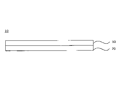
[0016] In its broad and varied embodiments, there is disclosed an optical
device 10
including a substrate 20; and at least one coating 30 applied to the substrate
20; in which the
optical device 10 has a first side exposed to an environment and a second side
that is unexposed,
as shown in FIG. 1. An "exposed" first side means facing the environment, such
as light, air,
dirt, wind, etc. An "unexposed" second side means not facing the environment
and can include
being applied to another device, such as a window, a sensor (e.g. LIDAR
sensor), or a lens, for
example, a self-standing optical lens, or a lens as part of a complex optical
system.
[0017] The disclosed optical device 10 can include at least one coating 30
that can
protect another device, as disclosed above, against mechanical, optical,
chemical and
environmental factors. The at least one coating 30 can provide at least one
function. The at least
one coating 30 can include one or more coatings in order to provide multiple
functions to the
optical device 10. Additionally, the at least one coating 30 can include one
or more coatings 30
3
CA 3031650 2019-01-25
on an exposed first side and/or on an unexposed second side of the substrate
20 in order to
optimize the functions of each coating 30 of the optical device 10.
[0018] The substrate 20 of the optical device 10 can be any material
capable of being
coated. Non-limiting examples of substrates 20 include plastics, synthetic
sapphire, glass,
synthetic diamond, optical ceramic materials, optical quality polymers, and
light transmitting
substrates with absorption spectra as required by the functional application
of the optical device
10, such as silicon. Optical quality polymers include polycarbonates,
arcylates, and cyclic olefin
polymers. Various types of glass can be used including chemically strengthened
glass.
[0019] In an aspect, as shown in FIG. 6, the optical device 100 can
include more than one
substrate 110a, 110b. The inclusion of more than one substrate 110a, 110b can
improve the
safety of the optical device 100 and the sensor it is applied thereon.
Additionally, the inclusion
of more than one substrate 110a, 110b in the optical device 100 can increase
the structural
strength and/or flexibility of the optical device 100. The optical device 100
can include two or
more substrates 110a, 110b. The two or more substrates 110a, 110b can be a
laminate with two
or more substrates 110a, 110b fixed together. In an aspect, an adhesive can be
included between
the two more substrates 110a, 110b to form the laminate. A laminate substrate
can provide a
thinner and stronger optical device 100. However, the thickness of a single
substrate or a
laminate substrate is not a limiting factor in selecting a substrate suitable
for the optical device
100.
[0020] The at least one substrate 110a, 110b, can be the same or
different. In an aspect, a
first substrate 110a can be manufactured from hard optical materials ranging,
depending on
application and location, from chemically strengthened glass to inherently,
extremely hard and
impact resistant materials, such as synthetic sapphire or diamond. The first
substrate 110a can
4
CA 3031650 2019-01-25
include coatings 30 providing mechanical and protective functions on the first
exposed side and
can include a second substrate and/or coatings 30 providing optical functions
on the second
unexposed side. A second substrate 110b can function as a carrier of optical
coatings that can
provide additional protective functions to the optical device 10.
[0021] The substrate(s) 20, 110a, 110b, for use in the optical device 10,
100 can be
selected based upon safety, cost, weight, etc. The selection of the substrate
20, 110a, 110b is a
variable in the formation of the optical device 10, 100. In particular, the
selection of the
substrate(s) 20, 110a, 110b can change the order of layers of coatings 30 in
the optical device 10,
100.
[0022] FIGs. 2-5 illustrate various optical devices 10 contemplated
herein. These are
exemplary in nature. It should be appreciated that the order of the coatings
on the first exposed
side and the second unexposed side can vary. Additionally, the types of
coatings present on the
first exposed side and the second unexposed side can vary. Generally, the
coatings 30 that can
provide a mechanical or protective function are present on the first exposed
side of the optical
device and the coatings that can provide an optical function are present on
the second exposed
side of the optical device. The coatings 30 of FIGs. 2-5 are described more
fully below.
[0023] As shown in FIG. 2, there is illustrated an optical device 10
including on a first
exposed side an antireflective coating with anti-smudge treatment 30a, a
substrate 20, and on a
second unexposed side an electrical conducting coating 30b, and a glare
reducing coating 30c.
[0024] As shown in FIG. 3, there is illustrated an optical device 10
including on a first
exposed side an antireflective coating with anti-smudge treatment 30a, a
substrate 20, and on a
second unexposed side an electrical conducting coating 30b, a glare reducing
coating 30c, and an
antireflective coating 30e.
CA 3031650 2019-01-25
[0025] As shown in FIG. 4, there is illustrated an optical device 10
including on a first
exposed side an antireflective coating with anti-smudge treatment 30a, a
substrate 20, and on a
second unexposed side an electrical conducting coating 30b, a bandpass filter
30d, and a glare
reducing coating 30c.
[0026] As shown in FIG. 5, there is illustrated an optical device 10
including on a first
exposed side an antireflective coating with anti-smudge treatment 30a, a
substrate 20, and on a
second unexposed side an electrical conducting coating 30b, a bandpass filter
30d, a glare
reducing coating 30c, and an antireflective coating 30e.
[0027] The optical device 10 can include a coating 30 applied to the
substrate 20, such as
an antireflective coating 30e. In an aspect, the antireflective coating 30e
can be present on the
first side of the optical device 10. The antireflective coating 30 can also be
treated to confer an
anti-smudge 30a property, as shown in FIGS. 2-5. In another aspect, the
antireflective coating
30e can be present on the second side of the optical device 10, as shown in
FIGs. 3 and 6. The
optical device 10 can include an antireflective coating with an anti-smudge
treatment 30a on a
first side and an antireflective coating 30e (without an anti-smudge
treatment) on the second
side.
[0028] An antireflective coating 30e can be a dielectric stack and can
reduce the light
reflection on an interface with the substrate 20. Suitable dielectrics for
forming the dielectric
stack include metal oxides such as TiO2, Ta205, ZrO2, and SiO2, which are
optically isotropic
and ca exhibit high transparency in the visible wavelength spectrum range
(e.g., from 400nm to
700nm). The antireflective coating 30e can be a stack including a first
plurality of dielectric
layers having a first refractive index, such as a low refractive index, for
example, SiO2 or
magnesium fluoride (MgF2), interleaved with at least a second plurality of
dielectric layers
6
CA 3031650 2019-01-25
having a second refractive index, such as a high refractive index. Non-
limiting examples of high
refractive index materials include niobium oxide, tantalum oxide, aluminum
oxide, titanium
oxide, zirconium oxide, and their combinations.
[0029] The antireflective coating 30e can be formed of a stack of layers of
NbTiOx, SiO2,
or the like. In an aspect, the antireflective coating 30e can be a thin film
dielectric stack of a first
layer of NbTiOx of about 50 nm, a first layer of SiO2 of about 18 nm, a second
layer of NbTiOx
of about 16 nm, a second layer of SiO2 of about 101 nm.
[0030] The optical device 10 can include a coating 30 applied to the
substrate, such as a
protectant coating. The protectant coating can be present on the first side of
the optical device.
The optical device 10 can include the protectant coating alone or in
combination with the
antireflective coating 30e. In an aspect, the protectant coating is applied to
an antireflective
coating 30e, which is applied to the substrate 20. The protectant coating and
the antireflective
coating 30e are both on the first side of the optical device 10.
[0031] In an aspect, the protectant coating can include a fluorinated alkyl
ether polymer
having a functionalized silane. An example of such a compound has the general
formula: Rrn¨
S i¨Xn (1), where R includes the fluorinated alkyl ether repeat unit, X can
be an alkoxy
group, a chloride, or an amine group, in which m + n equals 4. For example,
poly(perfluoropropyl ether) functionalized with a tri-methoxy silane group and
poly(perfluoroethyl ether) functionalized with a silazane group, are two such
compounds.
[0032] A protectant coating can be durable and can include a compound
having the
simplified formula: CF3¨[CH(CF3)¨CH2-0¨]x---CONCH3¨(CH2)3¨Si¨(0C2H5)3 (2)
where x is an integer from 7-11. This compound can also include a divalent
linking group (i.e.,
CONCH3 __ (CH2)3 __ ). Of course, compounds similar in structure and function
to that shown
7
CA 3031650 2019-01-25
in formula (2) can also be used in the protectant coating. In particular, both
N-methyl-N-(-
triethoxypropy1)-24a-heptafluoropropoxy {Poly(oxy(trifluoromethyl)-1,2-
ethanediy1)}tetrafluoropropionamide, commercially available compounds, can be
used in the
protectant coating.
[0033] Methods of applying the protectant coating can include wet
techniques such as
dipping, flowing, wiping, and/or spraying the surface with a liquid, solution,
or gel-like carrier
containing the coating compound, and dry techniques such as vapor coating the
coating
compound onto a surface (either at ambient pressure or under vacuum).
[0034] The optical device 10 can include a coating 30 applied to the
substrate 20, such as
an electrical conducting coating 30b, as shown in FIGs. 2-5. The electrical
conducting coating
30b can be present on the second side of the optical device 10. The electrical
conducting coating
30b can be a low surface energy treatment that serves as a soil, water, and
dust repelling surface.
This coating 30b can have a low coefficient of friction, such as less than
0.08. In this manner, the
electrical conducting coating 30b can reduce the susceptibility of the optical
device 10 to being
damaged by an abrasive media.
[0035] The electrical conducting coating 30b can include indium tin oxide
(ITO), nano-
particles based transparent composites, and other commonly used optically
transparent
conductors. In an aspect, the electrical conducting coating 30b can be
transparent at a
wavelength of operation of a LIDAR sensor, such as between about 850 nm to
about 2000 nrn.
[0036] The electrical conducting coating 30b can act as a heating element
to increase a
temperature of the optical device 10, such as from about 30 C to 80 C. As a
heating element, an
optical device 10 including this coating 30b can be used to eliminate and/or
reduce at least one
of: the risk of fogging of a window with an attached sensor, risk of moisture
condensation, and
8
CA 3031650 2019-01-25
increase soil repellency of the first exposed side of the optical device 10.
[0037] Additionally, this electrical conducting coating 30b can increase
the
hydrophobicity and oleophobicity of an outer antirefiective coating 30 on a
first side of the
substrate by increasing the efficiency in repelling water and contaminants.
[0038] The electrical conducting coating 30b may not be mechanically
durable enough to
create a robust surface. For this reason, the electrically conducting coating
30b should be
applied to the second side, i.e. the side of the optical device facing the
sensor.
[0039] The optical device 10 can include a coating 30 applied to the
substrate 20, such as
a glare reducing coating 30c. The glare reducing coating 30c can be present on
the second
unexposed side of the optical device 10, as shown in FIGs. 2-5. The glare
reducing coating 30c
and an electrical conducting coating 30b can both be present on the second
unexposed side of the
optical device 10. In an aspect, the glare reducing coating 30c can be applied
to an electrical
conducting coating 30b, which is applied to the substrate 20.
[0040] An example of a glare reducing coating 30c can be a multi-layer
structure of a
circular polarizer including a linear polarizer combined with a quarter wave
optical retarder.
Wave retarders are birefringent materials that alter (retard) the polarization
state or phase of light
traveling through them. A wave retarder has a fast (extraordinary) and slow
(ordinary) axis. As
polarized light passes through a wave retarder, the light passing through the
fast axis travels
more quickly through the wave retarder than through the slow axis. In the case
of a quarter wave
retarder, the wave plate retards the velocity of one of the polarization
components (x or y) one
quarter of a wave out of phase from the other polarization component.
Polarized light passing
through a quarter wave retarder thus becomes circularly polarized. The glare
reducing coating
30c can reduce and/or eliminate glare at the wavelength of operation of the
sensor protected by
9
CA 3031650 2019-01-25
the optical device 10. The glare reducing coating 30c can also allow for
analysis of the
polarization state of a signal beam.
[0041] The optical device 10 can include a coating 30 applied to the
substrate 20, such as
a bandpass filter 30d. The bandpass filter 30d can be present on the second
unexposed side of
the optical device 10, as shown in FIGs. 4-5. The bandpass filter 30d can be
applied to the glare
reducing coating 30c, which can be applied to an electrical conducting coating
30b, which is
applied to the substrate 20. In an aspect, the bandpass filter 30d, glare
reducing coating 30c, and
the electrical conducting coating 30b can all be present on the second
unexposed side of the
optical device 10. In an aspect, the glare reducing coating 30c can be applied
to an electrical
conducting coating 30b, which is applied to the substrate 20.
[0042] The bandpass filter 30d can be realized by a full stack of
dielectric low and high
refractive materials. Each layer can be deposited as a quarter-wave (QW)
thickness at the
wavelength of the desired filter. Each partial-reflector, which may be
comprised of only a single
layer, is called a quarter-wave stack (QWS). The bandwidth of the filter is a
function of the
reflectance of quarter-wave stacks in the structure. The center wavelength of
the pass-band is
determined by the thickness of the spacer dielectric material. The dielectric
materials used for
the quarter and/or half-wave layers have indices of refraction in the range
1.3 to beyond 4Ø For
example, some suitable materials are: Magnesium Fluoride (1.38), Thorium
Fluoride (1.47),
Cryolite (1.35), Silicon Dioxide (1.46), Aluminum Oxide (1.63), Hafnium Oxide
(1.85),
Tantalum Pentoxide (2.05), Niobium Oxide (2.19), Zinc Sulphide (2.27),
Titanium Oxide (2.37),
Silicon (3.5), Germanium (4.0), and Lead Telluride (5.0). Other dielectric
materials would serve
as well. Besides that, the fully dielectric band pass filter 30d can also
combine anti-reflective
properties.
CA 3031650 2019-01-25
[0043] In an aspect, the bandpass filter 30d can be a polymeric coating
containing an
appropriate mixture of dyes to create required absorbance or a combination of
dielectric and
polymeric structures.
[0044] The bandpass filter 30d can allow a wavelength of light at which a
sensor operates
pass and can eliminate all other wavelengths. For example, the bandpass filter
30d can block
wavelengths in the visible and near IR spectral range, such as from about 400
to about 850 nm,
and can transmit wavelengths above 850 nm. In this manner, the bandpass filter
30d can reduce
and/or eliminate unwanted radiation from reaching a sensor attached to the
optical device 10.
[0045] The optical device 10 can be attached to another device to form an
optical system.
The other device can be a window, a sensor (e.g. LIDAR sensor), or a lens, for
example, a self-
standing optical lens, or a lens. The optical device 10 can be attached to the
other device using
conventional deposition processes.
[0046] A method of making an optical device 10 is also disclosed. The
optical device 10
can be formed using semiconductor processes.
[0047] A method of making an optical system is also disclosed. The optical
device 10
can be attached to another device by conventional deposition processes to form
the optical
system.
[0048] From the foregoing description, those skilled in the art can
appreciate that the
present teachings can be implemented in a variety of forms. Therefore, while
these teachings
have been described in connection with particular embodiments and examples
thereof, the true
scope of the present teachings should not be so limited. Various changes and
modifications may
be made without departing from the scope of the teachings herein.
[0049] This scope disclosure is to be broadly construed. It is intended
that this disclosure
11
CA 3031650 2019-01-25
disclose equivalents, means, systems and methods to achieve the devices,
activities and
mechanical actions disclosed herein. For each device, article, method, mean,
mechanical
element or mechanism disclosed, it is intended that this disclosure also
encompass in its
disclosure and teaches equivalents, means, systems and methods for practicing
the many aspects,
mechanisms and devices disclosed herein. Additionally, this disclosure regards
a coating and its
many aspects, features and elements. Such a device can be dynamic in its use
and operation, this
disclosure is intended to encompass the equivalents, means, systems and
methods of the use of
the device and/or article of manufacture and its many aspects consistent with
the description and
spirit of the operations and functions disclosed herein. The claims of this
application are
likewise to be broadly construed.
[0050] The description of the inventions herein in their many embodiments
is merely
exemplary in nature and, thus, variations that do not depart from the gist of
the invention are
intended to be within the scope of the invention. Such variations are not to
be regarded as a
departure from the spirit and scope of the invention.
12
CA 3031650 2019-01-25