Note : Les descriptions sont présentées dans la langue officielle dans laquelle elles ont été soumises.
Line Power Extension for Capacitor Size Reduction in AC-DC Converters
Field
This invention relates to AC-DC power adapters for portable electronic devices
such as
laptop computers and cellphones. In particular, this invention provides
circuits and methods that
extend the duration that the AC line provides power to the load in each line
cycle, so that the size
of an input capacitor can be reduced.
Background
Technologies associated with power adapters for devices such as laptop
computers and
cellphones are fast advancing as new protocols and devices are unveiled. In
addition to wide
voltage range and high efficiency, small size is a valued feature for power
adapters. With new
semiconductor materials and advances in fabrication, size of semiconductors
has been reduced
significantly. Passive components, which may occupy more than 80% of the
converter volume,
however, generally cannot be reduced in size. With the recent development of
USB Power
Delivery, power adapters are designed for 15-60 W. At such power level, power
factor
correction is not mandatory. Thus, a full bridge rectifier D1-D4 and a
buffering electrolytic
capacitor Cm as shown in Fig. 1 are often used to convert the 100-240 VAC
input into DC
voltage. In some compact designs, the bulk electrolytic capacitor may take as
much as a quarter
of the total converter volume. Thus, reducing the capacitor value and size can
have significant
influence on the converter size.
A prior approach to reduce the energy storage of C,, was proposed in Published
European Patent Application No. EP2750274A1. Compared to a conventional full
bridge
- 1 -
Date Recite/Date Received 2024-02-16
approach as shown in Fig. 1, that approach required an additional capacitor
and two additional
diodes, and more complex control logic, which increased cost and size of the
circuit, and
effectively cancelled much of the reduction in overall power converter size
that was achieved by
reducing the size of the input capacitor.
Summary
According to one aspect of the invention there is provided a power converter
circuit,
comprising: a rectifier circuit having first and second input terminals that
receive an AC input
voltage, and first and second output terminals that output a DC bus voltage; a
series circuit
connected across the first and second output terminals, the series circuit
comprising a switch
connected in series with an input capacitor; and a controller that controls
the switch so that the
switch is on at least during a period when a magnitude of the AC input voltage
is less than a
selected DC bus voltage, and the switch is off during a period when the
magnitude of the AC
input voltage is greater than the selected DC bus voltage and less than a peak
value of the AC
input voltage.
In one embodiment the controller controls the switch so that the switch is
turned off
when a capacitor voltage reaches a peak value of the magnitude of the AC input
voltage.
In one embodiment the controller controls the switch so that the switch is
turned off at a
selected time at or between a first instant when the magnitude of the AC input
voltage is a peak
value and a second instant when the magnitude of AC input voltage is equal to
the DC bus
voltage.
In one embodiment the controller controls the switch so that the switch is
turned on
when the magnitude of the AC line voltage decreases to the DC bus voltage.
In one embodiment the controller controls the switch so that the switch is
turned off
when the magnitude of the AC line voltage decreases to a selected voltage
lower than a peak
value of the magnitude of the AC input voltage.
In one embodiment the rectifier circuit comprises a full bridge rectifier
having four
diodes.
- 2 -
Date Recite/Date Received 2024-02-16
Embodiments may be for use with a DC-DC converter selected from a flyback
converter, a resonant converter, a Buck converter, a Buck-boost converter, and
a forward
converter.
In one embodiment the power converter further comprises a DC-DC converter that
receives the DC bus voltage and outputs a controlled DC voltage. The DC-DC
converter may
comprise a flyback converter, a resonant converter, a Buck converter, a Buck-
boost converter, or
a forward converter. In one embodiment the DC-DC converter comprises a flyback
converter.
In one embodiment the DC-DC converter comprises a resonant converter.
According to another aspect of the invention there is provided a method for
implementing a power converter, comprising: providing a rectifier circuit
having first and second
input terminals that receive an AC input voltage, and first and second output
terminals that
output a DC bus voltage; connecting a series circuit across the first and
second output terminals,
the series circuit comprising a switch connected in series with an input
capacitor; and controlling
the switch so that the switch is on at least during a period when a magnitude
of the AC input
voltage is less than a selected DC bus voltage, and the switch is off during a
period when the
magnitude of the AC input voltage is greater than the selected DC bus voltage
and less than a
peak value of the AC input voltage.
In one embodiment the method comprises controlling the switch so that the
switch is
turned off when a capacitor voltage reaches a peak value of the magnitude of
the AC input
voltage.
In one embodiment the method comprises controlling the switch so that the
switch is
turned off at a selected time at or between a first instant when the magnitude
of the AC input
voltage is a peak value and a second instant when the magnitude of AC input
voltage is equal to
the DC bus voltage.
In one embodiment the method comprises controlling the switch so that the
switch is
turned on when the magnitude of the AC line voltage decreases to the DC bus
voltage.
In one embodiment the method comprises controlling the switch so that the
switch is
turned off when the magnitude of the AC line voltage decreases to a selected
voltage lower than
a peak value of the magnitude of the AC input voltage.
- 3 -
Date Recite/Date Received 2024-02-16
In various embodiments, the method comprises using a DC-DC converter to
receive the
DC bus voltage and output a controlled DC voltage. In various embodiments, the
DC-DC
converter comprises a flyback converter, a resonant converter, a Buck
converter, a Buck-boost
converter, or a forward converter.
Brief Description of the Drawings
For a greater understanding of the invention, and to show more clearly how it
may be
carried into effect, embodiments will be described, by way of example, with
reference to the
accompanying drawings, wherein:
Fig. 1 is a schematic diagram of a conventional full bridge rectifier circuit
without
power factor correction, according to the prior art.
Fig. 2 is a diagram showing the full bridge rectifier conduction waveform for
the circuit
of Fig. 1.
Fig. 3 is a plot showing DC voltage on Cm = 100g for different AC input
voltages
(VAC rms) and 60 W load power, for the circuit of Fig.l.
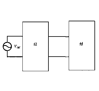
Fig. 4A is a diagram showing a power adapter connected to a portable
electronic device,
according to one embodiment.
Figs. 4B and 4C are diagrams showing line power extension circuits without and
with a
subsequent DC-DC converter stage, according to embodiments.
Fig. 5 is a diagram showing key waveforms for the circuit of Fig. 4B.
Figs. 6A-6C are schematic diagrams showing operation of the circuit of Fig. 4B
during
three time intervals, wherein dashed lines show parts of the circuit that are
not in operation
during each interval.
Fig. 7 is a circuit diagram showing a controller implemented for a line power
extension
circuit, according to one embodiment.
Fig. 8 shows the results of a simulation comparing the value of Cm required
for different
Vb.ili voltages, for a conventional full bridge and a line power extension
circuit according to
one embodiment.
- 4 -
Date Recite/Date Received 2024-02-16
Fig. 9 shows the results of a simulation comparing Vbus_mm at different values
of C., and
the gain required for a subsequent converter stage, for a conventional full
bridge and a line
power extension circuit according to one embodiment.
Fig. 10 shows the results of a simulation comparing current and loss of a
conventional
full bridge rectifier and a line power extension embodiment.
Figs. 11 and 12 show performance of a prototype line power extension circuit
operating at
60 W and 30 W loads, respectively.
Detailed Description of Embodiments
According to one aspect, the invention provides methods and circuits for
reducing the
value and size of an input electrolytic capacitor C. of an AC-DC converter, by
extending the
duration that the AC line provides power to the load in each line cycle.
According to
embodiments, which may be referred to herein as line power extension circuits,
the input
capacitor energy is used only when the AC voltage is below a selected level.
Capacitor
discharging is controlled by an auxiliary switch, while capacitor charging is
not changed relative
to a conventional circuit. As described herein, line power extension circuits
and methods may
reduce the input capacitor value and size significantly, relative to
conventional circuits, e.g., a
reduction of 33% in an embodiment operating at 60 W output power.
Alternatively, when a
capacitor value according to a conventional design is used, the DC bus voltage
range and the
current stress may be reduced, from which the design of a following stage
(e.g., a DC-DC
converter) may benefit. Embodiments are described in detail below with respect
to a full bridge
rectifier that converts an AC voltage to a DC voltage (e.g., Fig. 4B). The
output of the rectifier is
a DC voltage with voltage ripple dependent on the capacitor value and the
output power. A
subsequent DC-DC converter stage may be used to convert the DC voltage into a
controlled DC
voltage level (e.g., Fig. 4C). For example, a flyback converter, a resonant
converter, a forward
converter, a Buck converter, a Buck-boost converter, etc., may be used as the
DC-DC converter.
Advantageously, in the embodiments C. functions as both an output capacitor of
the line power
extension circuit and as an input capacitor of a subsequent DC-DC converter
stage. Thus, the
need for an additional input capacitor for the subsequent stage is avoided,
which reduces size and
cost of the AC-DC converter. Further, in the embodiments C. is not connected
directly across
- 5 -
Date Recue/Date Received 2024-02-16
the input terminals of the subsequent DC-DC converter stage, and no further
capacitors are
connected in parallel, thereby avoiding any possible current spike when the
auxiliary switch is
activated and the need for a current limiting inductor. In implementations
such as that shown in
Fig. 4A, it will be appreciated that a power adapter 42 incorporating an
embodiment as described
herein benefits from low component count, reduced component current stress,
reduced size and
weight, and low cost, making it suitable for a range of portable devices 44
such as laptop
computers and cellphones.
Capacitor Buffering
A conventional full bridge rectifier circuit without power factor correction
is shown in Fig.
1, and Fig. 2 shows the voltage and current waveforms. In Fig. 2, Ivnel is the
absolute value of the
AC line voltage, V bus is the voltage on the input capacitor Gn, lac is the
input current from the AC
line, and 0 is the conduction angle. Vbus_peak refers to the peak value of a
specific AC voltage.
For example, for 120 VAC, V bus _peak is 120 V*1.414 = 170 V; for 220 VAC,
Vnnseak _s _p i 220
V*1.414 = 310 V. V bus max refers to the absolute maximum value of all input
AC voltages
covering the range of 100-240 VAC, in other words, V bus _max is one fixed
value of 240 V*1.414 =
340 V. The same applies to V bus valley and V bus min (see Fig. 5). As an
example, V bus is the bus
voltage for a following DC-DC converter stage.
When V bus is lower than the line voltage, the capacitor will be charged until
it equals the
peak line voltage. After that, Cm will be discharged to power the load until
its voltage is lower
than the line voltage in the next half line cycle.
At a given AC voltage, the relationship between Vbus_penk and V bus valley is
determined by
(1), in which P, is the output power and At is the discharging time of Cm.
1 r,
¨2 Lin b2us_valley vb2us _ peak) = = At (1)
At may be found using equation (2), in whichfine is the AC line frequency. The
conduction
angle 8 is given in equation (3).
- 6 -
Date Recite/Date Received 2024-02-16
¨ 0
At = (2)
22-cfime
V
0 = cos,¨ .. bus_valley
(3)
V
bus peak
If the capacitor value is large enough so that the voltage drop (i.e.,
Vbus_peak - Vbus_yalley)
can be neglected, then the capacitor discharging time is approximately
1/2fine. Based on this
.. assumption, the DC voltage range on Cui at different AC voltages may be
calculated. For
example, Fig. 3 shows the DC voltages on a 100 !IF capacitor for 60 W power at
different AC
voltages from 100-240 VAC. As one example, when the input voltage VAC is about
100 Vrms,
the DC voltage across the 100 uF capacitor will vary from about 100 to 141
VDC. When the
input voltage VAC is 200 Vrms, the DC voltage across the 100 uF capacitor will
vary from about
.. 261 to 283 VDC.
As shown in Fig. 3, for universal AC input from 100 ¨ 240 VAC, the maximum Cm
voltage Vbus max is about 340 V, which is the peak voltage at 240 VAC (i.e.,
240 V x 1.414 =
339.34 V). On the other hand, the minimum G voltage Vbusinin is determined by
the valley
voltage point at 100 VAC. For a given power level, Vb., varies for different
Cin values. In this
.. case, with 60W load and Cm = 100 F, Vbus_min is 100 VDC, at which the
converter has
maximum current stresses.
For 100 VAC, if the minimum DC voltage Vbus ml,, is chosen as 100 V, the
conduction
angle 0 (as shown in Fig. 2) is only 45 in a half line cycle (i.e., 25% of
the cycle period). The
input capacitor provides the power for the remaining 1350 of the half line
cycle (i.e., 75% of the
cycle period). Accordingly, the input capacitor must be of a large value,
which translates to a
large physical size.
According to one aspect of the invention, drawbacks of the conventional full
bridge
approach described above are overcome by extending the time that the AC line
voltage is used to
power the load. When the AC line provides more power to the load, the input
capacitor does not
.. need to store as much energy as in the conventional full bridge case. As a
result, the capacitor
value can be reduced while achieving same bus voltage range.
Referring to the conventional circuit of Fig. 2, it is noted that the AC line
provides
- 7 -
Date Recite/Date Received 2024-02-16
power only before the peak voltage, even though after that the line voltage is
still higher than the
V bus mm. However, according to embodiments of the invention, the interval
after the peak point
(i.e., after Vb.seak, until _p V
bus mzn is also used, increasing the conduction angle 0. A controller
controls the extent to which the conduction angle is increased. In some
embodiments, 0 is
doubled, relative to the conventional case. Effectively, the capacitor
discharging time is reduced.
Thus, the required capacitor value can be reduced to achieve the same Vbus
min. Alternatively,
with the same capacitor value as in a conventional design, Vb. mm can be
increased. In
applications where a subsequent DC-DC converter stage is used, the voltage
gain requirement for
the DC-DC stage is reduced, which also reduces the current stress. These
features translate into
an efficiency improvement or an overall reduction in size of the converter.
Fig. 4B shows an embodiment, referred to herein as a line power extension
circuit,
including a full bridge rectifier circuit rectifier D1-D4 and switch S
connected in series with
capacitor C. S is connected in such a way that the current through the body
diode will charge
the capacitor Cm. Thus, regardless of the state of S, Cm is always charging
when the line voltage
is higher than the capacitor voltage. Cui is discharged only when S is turned
on.
Fig. 5 shows key waveforms of the embodiment of Fig. 4B. In Fig. 5, V bus is
the output
voltage of the line power extension circuit, as well as the input voltage for
a subsequent stage
(e.g., a DC-DC converter stage). Ivacl is the absolute value of the AC input,
la, is the AC input
current, and Gs is the gate signal of the switch S. Figs. 6A-6C show three
states A, B, and C of
operation of the embodiment during the positive half line cycle, wherein
dashed lines show parts
of the circuit that are not in operation. Operation during the negative half
cycle is similar to that
shown in Figs. 6A-6C.
State A [to, N.- DI and D4 start to conduct at to, at which time vac equals
Vbus . From to to
ti, the capacitor voltage increases with vac. During this time, S is turned
on, in order to reduce
conduction loss. In an ideal case, S is turned off at ii, at which time the
capacitor voltage reaches
the peak value. However, in practice, S may be turned off at a selected time
between to and ti to
achieve optimal performance. The capacitor continues to be charged through the
body diode of S
to the peak line voltage.
State B 12]: At Ii, the input AC voltage reaches peak value and
the capacitor Cin is
also charged to peak value. After ii, the AC voltage will be lower than the
peak value. As S turns
- 8 -
Date Recite/Date Received 2024-02-16
off at ii, the capacitor is disconnected from the load, thus the capacitor
voltage remains as the
peak line voltage. The load is powered by the AC line directly during ti to
12, and the AC current
is the AC voltage divided by the load resistance. Due to this extended
conduction time, lac is
lower than the conventional full bridge. During ti to 12, the body diode of S
is reverse-biased. The
peak voltage stress on S is reached at 12, and is equal to Vbus max¨ Vbus mm.
Generally, in
embodiments operating with input voltage of 100-240 VAC, the voltage stress is
below 100 V. It
is noted that the switch S is operated (i.e., turn-on and turn-off) when the
input AC voltage is
low. The voltage stress on S is the difference between the peak AC voltage
(e.g., 141 V for 100
Vrms AC input) and the Vbus nun (e.g., 100 V). In this example, the voltage
stress is 41 V (141 ¨
100 V). When the input AC voltage is high, the switch S is always turned on.
Therefore, a
switch such as a MOSFET with voltage rating of 100 V may be used for S.
State C [12, 13] : After 12, Vac reduces below the designed Vbusmin. S is
turned on at/2, so
that the capacitor energy is used. As the capacitor voltage is maintained at
the peak line voltage,
Di and D4 will be reverse-biased after 12. The capacitor voltage will decrease
until it is equal to
Vac. In this case, the capacitor value is selected such that the minimum
capacitor voltage at 13 is
equal to the line voltage at 12, both at Vbus
Controller
An embodiment including a controller is shown in Fig. 7. In this embodiment
the
controller includes a circuit 72 used to determine the operation mode of the
control circuit, i.e.,
whether line power extension is needed (i.e., activated, the switch is off).
Line power extension
control is activated when the magnitude of the AC voltage is low, i.e., below
Vims mm; for
example, 100 VAC. For normal operation at, e.g., 120 VAC, the bus voltage
should always be
higher than the designed Vb. min. Thus, there is no need to activate line
power extension and the
switch remains on, and the circuit operates substantially equivalent to a
conventional full bridge
rectifier.
The controller also includes a circuit 74 used to determine on/off timing of
the switch S.
In an ideal case, S should be turned off at the line voltage peak (i.e.,
Vb.ipeak) 1 after which the line
will power the load directly. The turn-on timing of S is when the magnitude of
the line voltage
decreases to a designed Vb._mbi.
- 9 -
Date Recite/Date Received 2024-02-16
Performance Comparison
A simulation was conducted using PSIM (Powersim Inc., Rockville, MD, USA) to
determine the required capacitance value of C1 for a line power extension
embodiment and a
conventional full bridge, for designs based on different Vbus_min and a 60 W
load. Fig. 8 shows
simulation results.
As shown in Fig. 8, when Vbus_min is set at 50 V, then a 37 F capacitance
should be
used for a conventional full bridge diode rectifier, while only 15 1.1F is
needed for a line power
extension embodiment. Thus, a 59% capacitor reduction is achieved for a 50 V
design. The
capacitor reduction ratio, shown by the solid line in Fig. 8, decreases as
Vbus nun increases, as the
AC power conduction angle is reduced. In practice, a typical Vbus min design
is 90-100 V, at
which the capacitance can be reduced by about 33% with line power extension as
described
herein, relative to a conventional full bridge diode rectifier.
When a line power extension embodiment is implemented with the same
capacitance as
a conventional full bridge diode rectifier, then Ilbus ,,,,,, can be increased
to relieve the wide
voltage gain requirement for a following DC-DC converter stage. Fig. 9 shows
the results of a
simulation comparing the minimum bus voltage between a conventional full
bridge circuit and a
line power extension circuit for different C,õ values. As shown in Fig. 9, in
an extreme case
where a 39 p.F capacitor used, then Vbus min for the full bridge is only 55 V,
while that for the line
power extension circuit is 86 V. When Vbus mar is 340 V, the normalized
voltage gain
requirement is reduced from 6.2 to 4 (i.e., 340 V/55 V = 6.2; 340 V/86 V = 4).
That is, the
voltage gain requirement for a subsequent DC¨DC converter is reduced to only
64% (4/6.2 =
64%) of that in the conventional full bridge. As shown in Fig. 9, as the value
of C,,, increases,
the difference in Vbusimin decreases (due to the conduction angle decreasing),
thus the line power
extension circuit produces less reduction in the required voltage gain.
In a practical case, if an 82 tiF capacitor is used, then Vbus_min can be
increased from 99
V in a conventional full bridge to 108 V with the line power extension
circuit, which is an ¨10%
improvement. For a following DC-DC converter, e.g., a series resonant
converter, this 10%
voltage improvement indicates the same amount of current stress reduction.
Then, the
conduction loss can be reduced to only ¨80% (= 0.92) of that in the
conventional full bridge case.
Besides a significant current reduction for the following DC-DC converter,
current
- 10 -
Date Recue/Date Received 2024-02-16
stress in the input rectifiers is also reduced with a line power extension
circuit as described
herein. Fig. 10 shows the results of a simulation comparing current stress and
loss of a
conventional full bridge rectifier and a line power extension circuit. In Fig.
10, I ave diode:
average current in diodes D1-D4; I_rms_ESR: RMS current in Cm; P_diode: power
loss diodes
D1-D4; P ESR: power loss in Cm; P dson: conduction loss in switch S; P total:
total power loss.
In this example the diode loss was calculated based on 0.95 V forward voltage
drop for a bridge
rectifier (e.g., Micro Commercial Components, Part No. LB6S), while the MOSFET
conduction
loss P as. was calculated based on Ras. of 85 mOhms (e.g., STMicroelectronics,
Part No.
STF43N6ODM2). It can be observed that the diode bridge has significantly
higher loss as
compared to the additional switch. The extra loss created by the additional
switch can be
compensated by the reduced current stress in the diode bridge, so that the
total loss P _total in the
conventional circuit and the line power extension circuit are same in this
example. However, if
the losses in the EMI filter are also considered, then the line power
extension circuit reduces the
total loss.
Working Example
A 60 W prototype was built according to the circuit of Fig. 4B and the
parameters
shown in Table 1. For Cm, a total of 60 F (56 jif electrolytic + 4.7 tiF
ceramic) capacitance is
needed to maintain Vbus mIn at 100 VDC for 100 VAC. As a comparison, 85 RF (82
[IF
electrolytic + 3.3 tiF ceramic) should be used to achieve same input voltage
range.
- 11 -
Date Recue/Date Received 2024-02-16
Table 1. Design parameters.
Input AC voltage 100¨ 240 VAC
Operation of Line Power Extension 100 VAC
Operation as Fun Bridge 110 ¨ 240 VAC
Output Power 60 W
Input Capacitor Cin 56 tiF (electrolytic)+ 4.7 pF (ceramic)
Minimum Bus Voltage Vbusmin 100 VDC
Rdson = 85 mOhms (e.g., STMicroelectronics,
Auxiliary MOSFET
Part No. STF43N6ODM2)
Forward voltage drop = 0.95 V (e.g., Micro
Diode Bridges
Commercial Components, Part No. LB6S)
dsPIC33FJ06GS101A (e.g., Microchip
Controller
Technology Inc.)
Auxiliary MOSFET Driver PC817 (e.g., Sharp/Socle Technology)
The sizes of 56 p,F and 82 F electrolytic capacitors (Rubycon BXW series) were
compared. Both capacitors had the same diameter of 16 mm. The length of the
561,LF capacitor
was 21 mm, while that of the 82 tiF capacitor was 31 ram. Thus, a 30% (1
¨21/31 = 30%)
capacitor size reduction was achieved with the line power extension circuit.
Fig. 11 shows key waveforms under 100 VAC input and 60 W load power. The
minimum value of Vi, us is controlled at 100 V. For a 60 W load, the peak AC
current stress is 3.6
A.
Fig. 12 shows key waveforms under 100 VAC input and 30 W load power. At this
power level the minimum value of vbõ, is controlled at 100 V. It can be seen
from the waveform
of Vbus that with a 30 W load, the voltage variation across Cin is smaller
than with a 60 W load
(Fig. 11).
- 12 -
CA 3034422 2019-02-20
Equivalents
While the invention has been described with respect to illustrative
embodiments thereof,
it will be understood that various changes may be made to the embodiments
without departing
from the scope of the invention. Accordingly, the described embodiments are to
be considered
merely exemplary and the invention is not to be limited thereby.
- 1 3 -
CA 3034422 2019-02-20