Note : Les descriptions sont présentées dans la langue officielle dans laquelle elles ont été soumises.
SINGLE STAGE CURRENT CONTROLLER FOR A
NOTIFICATION APPLIANCE
TECHNICAL FIELD
The present disclosure relates generally to current controllers for
notification
systems, and more specifically to a single stage current controller for the
same.
BACKGROUND
Fire alarm and mass notification systems are used to notify the public of the
presence of fire, smoke and other potentially harmful conditions. A
notification
appliance circuit (NAC) may be part of such a system and include many
notification
devices powered and controlled by a common power source and control panel.
A notification appliance for providing audio and/or visual notifications to
draw attention to an incident and/or an announcement, such as a strobe based,
horn
based, or combination of strobe and horn based notification system (depending
on the
components of the notification appliance), may be utilized as part of a NAC
and is a
warning device with a light engine, an energy store and a flash control.
Strobes that
are part of a NAC are required to flash in a synchronized manner. The strobe
notification appliance provides a brief intense flash of light at
predetermined
intervals. The brief intense flash from many different strobes requires more
power
than is practically provided over the circuit.
Key performance metrics for a notification strobe are cost, current-draw and
reliability. With regards to the current-draw metric, two current components
must be
used over the course of operations. First is the initial current draw when the
strobe
begins operating, and the second is the normal operational draw as the strobe
maintains operations. The continuous draw is referred to herein as the
operating
draw of the notification appliance. Existing systems addressed the varied
current
requirements of the initial current draw and the operating draw by utilizing a
current
controller having multiple distinct hardware stages, with each hardware stage
providing the current for a different current draw component.
Utilization of multiple stages within a circuit increases the physical
component count, the required surface area of the circuit board, the cost, and
the
complexity of the current controller. Further, switching losses involved in
operating
1
CA 3037018 2019-03-15
switch mode converters can dominate the efficiency of the current controller
while
operating at low voltages.
SUMMARY OF THE INVENTION
In one exemplary embodiment a notification appliance circuit includes at
least one notification appliance. The at least one notification appliance
includes a
charge controller including a single stage current controller, the charge
controller
being configured to output a charge current, an energy store configured to
receive the
charge current, and provide a discharge current, and a notification component
configured to receive the discharge current and emit a notification.
In another example of the above described notification appliance circuit the
charge controller further includes a processor configured to provide the
single stage
current controller with a charge current control signal and an enable signal.
In another example of any of the above described notification appliance
circuits the processor includes a memory storing instructions configured to
cause the
processor to perform an adaptable optimized charging method.
In another example of any of the above described notification appliance
circuits a charge level output of the energy store is connected to the
processor.
In another example of any of the above described notification appliance
circuits the single stage current controller includes a current sensor
configured to
sense an input current of the current controller, a transconductance element
configured to output a charge current based on a magnitude of a received
transconductance control signal, and a main circuit configured to produce the
transconductance control signal based at least in part on a sensed current
value
received from the current sensor, a charge current control input, and an
enable input.
In another example of any of the above described notification appliance
circuits the transconductance element includes a MOSFET.
In another example of any of the above described notification appliance
circuits the sensed current value and the charge control current value are
connected to
a summation circuit configured to add the sensed current value and the charge
control
value.
In another example of any of the above described notification appliance
circuits at least one of the sensed current value and the charge control
current value is
2
CA 3037018 2019-03-15
connected to the summation circuit via one of a first gain circuit and a
second gain
circuit.
In another example of any of the above described notification appliance
circuits the sensed current value is connected to the summation circuit via a
first gain
circuit and the charge control current value is connected to the summation
circuit via
a second gain circuit.
In another example of any of the above described notification appliance
circuits the enable input is connected to a bias generator, and the bias
generator is
configured to generate a bias voltage based on the enable input.
In another example of any of the above described notification appliance
circuits an output of the summation circuit is connected to a summer, an
output of the
bias generator is connected to the summer, and the summer is configured to
subtract
the output of the summation circuit from the output of the bias generator.
In another example of any of the above described notification appliance
circuits an output of the summer is connected to an input of the
transconductance
element.
In another example of any of the above described notification appliance
circuits the charge controller is programmable.
An exemplary method for controlling a charge current of a notification
appliance includes receiving an input current at a single stage current
controller, and
outputting a charge current from the single stage current controller during at
least two
operational modes of the notification appliance.
In another example of the above described method for controlling a charge
current of a notification appliance the at least two operational modes include
an
operating draw mode and an initial current draw mode.
In another example of any of the above described methods for controlling a
charge current of a notification appliance outputting the charge current from
the
single stage current controller comprises providing a voltage input to a
transconductance element, and generating a current output from the
transconductance
element, wherein the current output is the charge current.
Another example of any of the above described methods for controlling a
charge current of a notification appliance further includes determining the
voltage
input based at least in part on a sensed input current of the single stage
current
3
CA 3037018 2019-03-15
controller, and a chargc current control signal output from a processor and an
enable
signal output from the processor.
Another example of any of the above described methods for controlling a
charge current of a notification appliance further includes multiplying at
least one of
the charge current control signal and the sensed input current by a gain
value, thereby
ensuring that the charge current control signal and the sensed input current
are at a
correct scale.
Another example of any of the above described methods for controlling a
charge current of a notification appliance further includes summing the sensed
input
current and the charge current control signal to create a summed value,
generating a
bias voltage based on the enable signal, and subtracting the summed value from
the
bias voltage and thereby generating a transconductance element control signal.
In another example of any of the above described methods for controlling a
charge current of a notification appliance outputting a charge current from
the single
stage controller comprises outputting a charge current from a transconductance
element.
These and other features of the present invention can be best understood from
the following specification and drawings, the following of which is a brief
description.
BRIEF DESCRIPTION OF THE DRAWINGS
Figure 1 is a block diagram of an example notification appliance circuit.
Figures 2-4 illustrate an exemplary current controller for utilization in the
notification appliance circuit of Figure I in sequentially greater detail.
Figure 5 schematically illustrates an exemplary circuit diagram of an
exemplary current controller for the notification appliance circuit of Figure
1.
DETAILED DESCRIPTION OF AN EMBODIMENT
Referring to Figure 1, an example notification appliance 10 includes a light
engine 14 that generates a brief, intense flash of light at a predetermined
interval. The
example notification appliance 10 is one of many notification appliances 10
that are
part of a notification appliance circuit (NAC) schematically shown at 12. Each
of the
notification appliances 10 that are part of the NAC 12 are required to flash
at the
same time. However, it is not practical for all of the appliances 10 to draw
the
4
CA 3037018 2019-03-15
amount of power required for a flash from the NAC power input 15 during the
short time
duration of each flash. Accordingly, each notification appliance 10 includes
an energy store
24 that buffers energy from the NAC power input 15 for the light engine 14.
Energy store
24 may include a super-capacitor, a capacitor or a battery, and/or any other
form of energy
storage.
A charge controller 26 includes a single stage current controller 28 and a
processor
30. The processor 30 controls flash timing for the flash. The processor 30 may
be a
processing chip, a microcontroller, a microprocessor, or a combination of any
of these and is
not limited to any particular processor configuration. The charging current 34
is adjusted by
.. the processor 30 that is part of the charge controller 26. In order to
control charge of the
energy store 24, the processor 30 provides current control using charge
current control 38
and an enable signal 39 connected to the single stage current controller 28.
The processor 30
includes a method that controls the charging current 34 which charges the
energy store 24.
The method can be an adaptable optimized charging method, as described in U.S.
Provisional Patent Application number 62/618,276. Alternatively, any other
method that
may be known in the art could be utilized in place of the adaptable optimized
charging
method depending on the needs of a specific implementation.
The energy store 24 is used to convert a long duration low power charge from
input
current 32 provided by the NAC power input 15 into the high power short
duration energy
discharge utilized by a notification component such as the light engine 14.
The energy store
24 is charged with a charging current 34 to generate the discharge current 36
to the
notification component, in this case the light engine 14. The charging current
34 must
charge the energy store 24 up to a fully charged level within a predetermined
interval at
which the light engine 14 operates. The energy store 24 is charged from a low
charge level
to a fully charged level required to power the light engine 14 and then
recharged within the
predefined interval of flashes for the next flash. In order to facilitate
these operations, a
charge level 40 of the energy stored is determined using any conventional
charge level
detection means and is provided to the processor 30.
During the discharge period of the predefined interval, the light engine 14
takes
power from the energy store 24 and uses a light driver 16 to convert that
power
5
Date Recue/Date Received 2020-10-08
into a form usable by a light source 18. The light source 18 generates light
conditioned through optics 20 to emit a desired light pattern 22.
The example charge controller 26 includes a processor 30 which includes a
control method that adjusts the charging current 34 such that the charge level
40 of
the energy store 24 is recharged to a full charge level required to generate
the light
flashes at a minimum output level and within a time that corresponds with the
predetermined interval. The charging can be performed according to the
adaptable
optimized charging method in some examples, as described in U.S. Provisional
Patent Application number 62/618,276. In alternative examples, the charging
can be
performed using any alternative charge method that may be known in the art.
In order to reduce the physical component count, reduce the size of each of
the notification appliances 10 within the NAC 12, and reduce the complexity of
the
single stage current controller 28, a single stage current controller 28 is
utilized to
provide the charge current 34 for both the operating draw and the initial draw
of the
energy store 24. The single stage current controller 28 replaces the inrush
limiter,
inrush bypass and current regulator systems of previous multi-stage current
controllers. Further, in some examples, the single stage current controller 28
is
programmable and capable of being programmed to output a substantial range of
current values, depending on the analog voltage of the charge current control
38
input received from the processor 30.
In some examples, the single stage current controller 28 is a linear current
controller, with the output current being linearly dependent upon the charge
current
control input 38. In such examples, the single stage current controller 28 has
a lower
rated current than existing switch-mode (multi-stage) current controllers
across the
rated voltage range of the single stage current controller 28.
The flexible current output design of the single stage current controller 28
allows the initial current draw for any given operation to be sculpted to the
desired
output rating. In yet further examples, the single stage current controller 28
can be
utilized in conjunction with an optimized adaptive charging method, performed
by
the processor 30, that continuously tunes the current output by the single
stage
current controller 28 to provide for optimized performance of the notification
appliance 10.
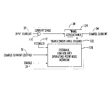
With continued reference to Figure 1, Figures 2-4 illustrate an exemplary
single stage current controller 28 for utilization in the notification
appliance 10 of
6
CA 3037018 2019-03-15
Figure 1 in sequentially greater detail. At the most general level,
illustrated in Figure
2, the single stage current controller 28 includes a current sensor 110 that
senses the
input current 32, and provides the sensed input current 32 to a main circuit
120 via a
feedback signal 112. The main circuit 120 can, alternatively, be referred to
as a
feedback control and operating-point-bias network because it is a circuit that
biases
the transconductance element 124 into conduction, and implements feedback
control
to hold the charge current at a level commanded by the charge current control
signal
despite perturbations away from nominal component values caused by tolerance
or
thermal effects.
The main circuit 120 also receives the charge current control signal 38, and
the enable signal 39, and converts the three received signals 38, 39, 112 into
a
transconductance control signal 122. The transconductance control signal 122
is
output to a transconductance element 124 which controls the magnitude of the
charging current 34 output from the single stage current controller 28.
Transconductanee is the electrical characteristic relating the current through
the output of a device to the voltage across the input of the device, and can
alternately be referred to as mutual conductance. The transconductance control
signal 122 provides a voltage to an input of the transconductance element 124,
with
the magnitude of the voltage controlling the output current (the charging
current 34)
of the transconductance element 124. In one exemplary embodiment, illustrated
in
Figure S. the transconductance element 124 comprises a MOSFET transistor. In
alternative embodiments, any alternative transconductance element 124, or an
arrangement of transconductance elements, can be utilized to the same effect.
Although biasing may not be required of an ideal transconductance element,
biasing is a requirement of a real-world MOSFET. A MOFET sets the gate-source-
voltage (Vgs) above its threshold (Vgs-th), to allow current flow between the
source
and drain. Biasing to the operating point is an attempt to set the MOSFET
towards a
linear region of the Vgs / Id curve. Feedback is used to overcome non-
linearity in
component characteristics (as occurs with production tolerance between
components,
and within an individual component as ambient and self-heating temperature
change).
Within the main circuit 120, a summation block 121 combines the feedback
signal 112 from the current sensor 110 with the charge current control signal
38, and
provides the control signal 127 to a summer 123. Simultaneously, the enable
signal
7
CA 3037018 2019-03-15
39 is provided to a bias generator 125 that creates a bias signal 129 based on
the
enable signal 39. The bias signal 129 and the control signal 127 are combined
in the
summer 123, with the control signal 127 being subtracted from the bias signal
129, to
form the transconductance control signal 122. The transconductance control
signal
122 is provided to the transconductance element 124, and controls the output
charging current 34.
Also included between the current sensor 110 and the summation block 121 is
a current sense gain 131. Positioned between the charge current control signal
38
and the summation block 121 is a charge current control gain 133. The gains
131,
133 multiplicatively adjust the sensor signal 112 and the charge current
control signal
38 to match the output characteristics of their respective preceding stages
with the
input characteristics of the summation block 121. The correct gain for any
given
main circuit 120 will depend on the application, and the actual components of
the
main circuit and can be determined using any known conventional means.
Gain is a requirement of real-world components in order to match the output
characteristics of the previous stage with the input characteristics of the
next stage.
In an exemplary embodiment, the processor 30 may output Charge Current Control
signal 38 by using a digital-to-analog converter (DAC) output with a range on
the
order of 0 to 3V and the summation block 121 may have an input range on the
order
of 0 to 1.0V, then a matching gain of 1.0/3,0 7-=,- 0.3 could be used between
the stages.
Thus the equation (voltage of Charge Current Control) * (Charge current
control
gain) ¨ summation block input, or [0 to 3.0V] * 1.0/3.0 = [0 to 1.0V];
therefore, the
range or outputs which the processor 30 may produce for the charge current
control,
0 to 3.0V, will be expressed for the range of inputs the summation block is
configured to accept, in this case, 0 to 1.0V. Thus, the scale required for
adjustment
of the current, e.g. the required gain between the charge current control 38
and the
summation block 121 may be determined from the output characteristics (e.g.
voltage
range) of the charge current control 38 and the input characteristics of the
summation
block 121. Similarly, if the output range of the charge current control 38 is
similar to
the input characteristics of the summation block 121, no gain will be
required.
With continued reference to Figures 1-4, Figure 5 schematically illustrates a
circuit diagram of an exemplary single stage current controller 28 for
implementing
the notification appliance 10 of Figures 1-4. It is appreciated that
alternative
8
CA 3037018 2019-03-15
topologies for implementing the block diagrams of Figure 1-4 could be utilized
to
similar effect and still fall within the purview of this disclosure.
The exemplary single stage current controller 28, receives the input current
32 at a first node 201. The first node 201 is connected to a first end of a
first resistor
202 and a first transistor 204. The second end of the resistor 202 connects to
a
second node 203. Also connected to the second node 203 are a second resistor
206, a
third resistor 208, and the input of the transconductance element 124. The
third
resistor 208 connects the second node 203 to a third node 205. The third node
205 is
also connected to the second end of the first transistor 204, another input of
the
transconductance element 124, an input to a second transistor 210, and a first
capacitor 212. A control input for the first transistor 204 is connected to a
sixth node
211 and the sixth node 211 connects a third transistor 224 to the second
resistor 206.
The enable signal 39 is input to a fourth resistor 214, which is connected to
a
fourth node 207. A second capacitor 216 and a fifth resistor 218 each connect
the
fourth node to ground (neutral). The output of the second transistor 210 is
also
connected to ground via a sixth resistor 220.
"Fhe charge current signal 38 is received at a seventh resistor 222. The
seventh resistor 222 is connected at the opposite end to a fifth node 209. The
fifth
node 209 is connected to a control input of a third transistor 224, and is
connected to
ground via a third capacitor 226. The output of the third transistor 224 is
connected
to ground via an eighth resistor 228.
As described above, the single stage current controller 28 utilizes only a
single stage of electronics to achieve the desired charge current in all
operating
modes. Further. while the specific topology illustrated in Figure 5 can be
used to
achieve the system, it is understood that the system is not limited to the
exact
topology described.
It is further understood that any of the above described concepts can be used
alone or in combination with any or all of the other above described concepts.
Although an embodiment of this invention has been disclosed, a worker of
ordinary
skill in this art would recognize that certain modifications would come within
the
scope of this invention. For that reason, the following claims should be
studied to
determine the true scope and content of this invention.
9
CA 3037018 2019-03-15