Note : Les descriptions sont présentées dans la langue officielle dans laquelle elles ont été soumises.
CA 03037460 2019-03-19
LIGHT SHAPING APPARATUS
Technical Field
[0001] The technique disclosed in the Description relates to a light shaping
apparatus
that uses a semiconductor laser device.
Background Art
[0002] Projectors and other equipment use, as their light sources, solid-
state light sources
(e.g., light-emitting diodes) in addition to discharge lamps (e.g., super-high
pressure
mercury lamps or xenon lamps).
[0003] Moreover, laser light sources with long life, low power consumption,
high
luminance, and high color purity have been recently used as the projectors'
light sources.
[0004] To obtain a desired optical output, large projectors for digital cinema
and other
purposes are provided with additional laser light sources, thus achieving a
high output.
Unfortunately, such addition involves projector upsizing or high manufacturing
cost.
Accordingly, optical-output enhancement per laser light source and component
downsizing
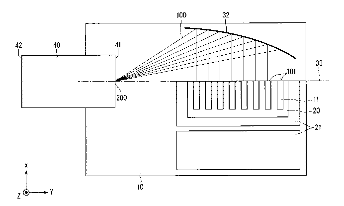
are required.
[0005] Further, semiconductor lasers, which are one example of the laser light
source,
emit light usually having an ellipsoid shape. The emitted light diverges at
approximately
8 degrees in the full-width at half-maximum in the slow-axis direction along
an active layer,
.. and diverges at approximately 30 degrees in the fast-axis direction
orthogonal to the slow-
axis direction.
[0006] An oscillation region or laser output window of each semiconductor
laser is
relatively narrow; its width in the fast axis, which is the thickness
direction of the active
layer, is 2 1AM or more and 10 pan or less. On the other hand, the width in
the slow-axis
CA 03037460 2019-03-19
2
direction along the active layer is several tens of micrometers or more and
several
hundreds of micrometers or less. Hence, the laser output window is a linear
light source
as a whole.
[0007] Light collimation is required in order to use the light emitted from
the
semiconductor laser as the light source of the projector. This collimation is
done by
shaping anisotropic light emitted from the linear light source, so that the
efficiency of
light use is enhanced in a projector optical system disposed at the posterior
stage of the
projector.
[0008] A collimator lens is inserted in a predetermined position in front of
the laser
.. output window. Since the laser output window is narrow in the fast-axis
direction,
collimated light is easily obtained through the collimator lens. Meanwhile,
this
collimator lens has difficulty in collimating light in the slow-axis
direction, in which the
laser output window is 10 times or more wider than in the fast-axis direction.
[0009] Collimating the light emitted from the laser output window whose width
is
greater in the slow-axis direction needs a separate collimator lens having a
long focal
length. Unfortunately, when a lens is provided to be distant away from the
laser output
window in order to adjust the focus of the collimator lens, beams of light
emitted from the
adjacent laser output windows interfere with each other before entering the
collimator
lens. Hence, it is difficult to shape individual beams of light properly.
[0010] To overcome this inconvenience, Patent Document 1, for instance,
(United
States Patent No. 5513201) proposes an optical member that shapes beams of
light in the
fast-axis direction, and then turns the individual beams of light by 90
degrees with respect
to the optical axis, followed by performing light shaping on the remaining
beams of light
in the slow-axis direction as light shaping in the fast-axis direction.
.. Prior Art Documents
CA 03037460 2019-03-19
3
Patent Documents
[0011] Patent Document 1: United States Patent No. 5513201
Summary
Problem to be Solved by the Invention
[0012] Patent Document 1 eliminates the need for a separate collimator lens
having a
long focal length to shape the light in the slow-axis direction. Patent
Document 1
achieves light collimation by shaping the light in the slow-axis direction
using a
collimator lens having a focal length as long as that of a collimator lens
used to shape the
light in the fast-axis direction. Further, since there is no need to provide a
collimator
lens having a long focal length, a long optical path is not necessary to shape
the two kinds
of light beam that travel in different directions.
[0013] The aforementioned method, however, requires an optical device, called
a
twister, that converts the fast-axis direction and the slow-axis direction
after the light
shaping in the fast-axis direction, and further requires performing of second-
time light
.. shaping in the fast-axis direction behind the optical device. Accordingly,
an optical
system that needs a long distance in the optical-axis direction as a whole,
has to be
formed.
[0014] To reduce manufacturing cost, the projectors' light sources are
strongly
required to be downsized. Thus, the aforementioned two-step light shaping,
which
involves an increase in the size of the light source, is not preferable.
[0015] The technique disclosed in the Description has been made to solve this
problem.
The technique relates to shaping light emitted from a linear light source
while preventing
mechanism upsizing.
Means to Solve the Problem
[0016] A light shaping apparatus according to a first aspect of the
technique disclosed
= CA 03037460 2019-03-19
4
in the Description includes a linear light source having at least one light-
emitting point, a
reflective mirror portion having a reflective surface that is an orthogonal
parabolic surface
formed by rotating a curved line about a rotation axis, and an optical device
disposed at a
convergence point where light emitted from the linear light source converges.
The light
emitted from the linear light source is reflected by the reflective mirror
portion
surrounding at least part of the linear light source, and further converges at
the
convergence point. The rotation axis of the reflective mirror portion extends
in the
longer-side direction of the linear light source. The light-emitting point of
the linear
light source is located on the rotation axis of the reflective mirror portion.
The optical
device has an entrance end face located at the convergence point. The entrance
end face
is an end face on which the light emitted from the linear light source is
incident.
Effects of the Invention
[0017] The light shaping apparatus according to the first aspect of the
technique
disclosed in the Description includes the linear light source having at least
one
light-emitting point, the reflective mirror portion having a reflective
surface that is an
orthogonal parabolic surface formed by rotating a curved line about a rotation
axis, and
the optical device disposed at a convergence point where light emitted from
the linear
light source converges. The light emitted from the linear light source is
reflected by the
reflective mirror portion surrounding at least part of the linear light
source, and further
converges at the convergence point. The rotation axis of the reflective mirror
portion
extends in the longer-side direction of the linear light source. The light-
emitting point of
the linear light source is located on the rotation axis of the reflective
mirror portion. The
optical device has an entrance end face located at the convergence point. The
entrance
end face is an end face on which the light emitted from the linear light
source is incident.
Such a configuration enables concentrating of light that diverges in the
longer-side
CA 03037460 2019-03-19
direction of the linear light source using the reflective mirror portion with
the reflective
surface, which is an orthogonal parabolic surface, thereby shaping the light
emitted from
the linear light source while preventing mechanism upsizing.
[0018] These and other objects, features, aspects, and advantages of the
technique
5 disclosed in the Description will become more apparent from the following
detailed
description of the Description when taken in conjunction with the accompanying
drawings.
Brief Description of Drawings
[0019] FIG. 1 is a schematic side view of a configuration for implementing a
light
shaping apparatus according to an embodiment.
FIG. 2 is a diagram illustrating a parabolic mirror according to the
embodiment.
FIG. 3 is a diagram illustrating an orthogonal parabolic mirror according to
the
embodiment.
FIG. 4 is a schematic plan view of a configuration for implementing the light
shaping apparatus according to the embodiment.
FIG. 5 is a schematic perspective view of a configuration for implementing the
light shaping apparatus according to the embodiment.
FIG. 6 is a schematic plan view of a configuration for implementing a light
shaping apparatus according to another embodiment.
FIG. 7 is a side view of a configuration for implementing a light shaping
apparatus according to a modification of the embodiment.
Description of Embodiment(s)
[0020] The embodiments will be described with reference to the accompanying
drawings.
[0021] The drawings are schematic; thus, for easy description, configurations
will be
= CA 03037460 2019-03-19
6
omitted or simplified as appropriate. In addition, the interrelationships of
the sizes and
positions of configurations illustrated on different drawing sheets are not
necessarily
exact, and thus can be changed as appropriate.
[0022] Throughout the following description, like components will be denoted
by the
same sings and will be provided with like names and like functions. Hence, the
detailed
description of the like components will not be elaborated upon for redundancy
avoidance
in some cases.
[0023] Throughout the following description, any terms, such as "top",
"under", "left",
"right", "side", "bottom", "front", and "back", that indicate specific
positions and specific
directions are used for the sake of easy understanding of the embodiments.
These terms
thus have nothing to do with actual directions when the embodiments are
practically
implemented.
[0024] <First Embodiment>
The following describes a light shaping apparatus according to a first
embodiment. Although the embodiment describes a semiconductor laser device as
one
example of a linear light source, the linear light source is not limited to
the semiconductor
laser device.
[0025] <Configuration of Light Shaping Apparatus>
FIG. 1 is a schematic side view of a configuration for implementing the light
shaping apparatus according to the embodiment. As illustrated in FIG. 1, the
light
shaping apparatus includes a stem 10, a semiconductor laser device 20 disposed
on the
stem 10 and having at least one light-emitting point, and a reflective mirror
portion 32
that is disposed on the stem 10 and substantially collimates light emitted
from the
semiconductor laser device 20.
[0026] FIG. 1 schematically illustrates, using arrows, laser light 100
travelling from an
CA 03037460 2019-03-19
7
exit end face 101, which is the light-emitting point of the semiconductor
laser device 20,
toward the reflective mirror portion 32. FIG. 1 illustrates laser light
divergence in the
Z-axis direction in FIG. 1, i.e., the fast-axis direction in FIG. 1.
[0027] The stein 10 is a plate member whose upper surface is provided with a
step.
The stem 10 is a metal stem base formed of a material having large thermal
conductivity
(e.g., Cu) whose surface is plated with Au and provided with a metallized
pattern. The
stem 10 fastens the semiconductor laser device 20 and the reflective mirror
portion 32,
and dissipates heat generated in the semiconductor laser device 20 to a cooler
(not shown)
below the stem 10.
[0028] The semiconductor laser device 20 is a laser diode having at least one
light-emitting point on an end face of a semiconductor chip of, for instance,
GaAs or
AlGaN. The laser light 100 is emitted from the light-emitting points of
the
semiconductor laser device 20 approximately along an optical axis
perpendicular to the
end face of the semiconductor chip and parallel to the upper surface or lower
surface of
the semiconductor chip, that is, approximately along the X-axis in FIG. 1.
[0029] Here, the junction between the stem 10 and the semiconductor laser
device 20 is
typically made by solder. In particular, AuSn solder, which has high
reliability and high
thermal conductivity, is desirably used.
[0030] The divergence angle of the light emitted from the semiconductor laser
device
20, in full, is about 80 degrees in the fast-axis direction. Accordingly, the
semiconductor laser device 20 is directly on the upper surface of the stem 10
in such a
manner that the exit end face 101 of the semiconductor laser device 20 is
placed in a
position flush with the side surface of the stem 10 or in a position slightly
protruding from
the side surface of the stem 10 so that the laser light 100 from the
semiconductor laser
device 20 does not hit the stem 10.
CA 03037460 2019-03-19
8
[0031] The reflective mirror portion 32, which is fastened by a retainer (not
shown), is
disposed in front of the exit end face 101 of the semiconductor laser device
20. The
reflective mirror portion 32 has an optical working surface or reflective
surface composed
of an orthogonal parabolic mirror.
[0032] FIG. 2 is a diagram illustrating a parabolic mirror. As illustrated in
FIG. 2, a
commonly known parabolic mirror has a curved surface, i.e., a parabolic
surface, formed
by rotating, about the X-axis, a curved line 30 whose XY cross-sectional
surface is
expressed by expression (1), where f denotes a focal length. This parabolic
surface is a
reflective surface.
[0033] [Numeral 1]
y2_.=4fx (1)
[0034] The parabolic mirror can collimate light 102 emitted from a point light
source
by concentrating the light 102 emitted from the point light source positioned
at the focal
point of the parabolic surface at its reflective surface, which is composed of
the parabolic
surface. Such a parabolic mirror is widely used as a mechanism that
concentrates light
from a lamp light source of a projector.
[0035] FIG. 3 is a diagram illustrating an orthogonal parabolic mirror. As
illustrated
in FIG. 3, the orthogonal parabolic mirror has a curved surface formed by
rotating, about
the Y-axis in FIG. 3, a curved line 31 whose XY cross-sectional surface is
expressed by
expressions (2) and (3), where f denotes a focal length. This curved surface
is a
reflective surface. Unlike the parabolic mirror, the orthogonal parabolic
mirror can
concentrate, onto one point, light 104 emitted from a linear light source 103
extending in
the Y-axis direction in FIG. 3.
[0036] [Numeral 2]
Y=2 x [f(f+X))1/2 (where -f_SA5_0 is satisfied) ... (2)
CA 03037460 2019-03-19
9
Y=2x(f(f¨X)11/2 (where 05_X5_f is satisfied) ... (3)
[0037] FIG. 4 is a schematic plan view of a configuration for implementing the
light
shaping apparatus according to the embodiment. FIG. 4 illustrates the behavior
of the
laser light 100 in the Y-axis direction, i.e., the slow-axis direction, in
FIG. 4.
[0038] As illustrated in FIG. 4, the semiconductor laser device 20 is a linear
light
source extending in the Y-axis direction in FIG. 4. The semiconductor laser
device 20 is
connected to a connecting substrate 21. The semiconductor laser device 20 has
a
plurality of waveguides 11 arranged at predetermined intervals. Each waveguide
11
extends in the X-axis direction in FIG. 4. The exit end faces 101 of the
waveguides 11
are arranged in the Y-axis direction in FIG. 4.
[0039] The reflective mirror portion 32 is disposed in front of the exit end
faces 101 of
the semiconductor laser device 20.
[0040] The dotted line in FIG. 4 denotes a rotation axis 33 of the orthogonal
parabolic
mirror of the reflective mirror portion 32. The rotation axis 33 extends in
the
longer-side direction of the semiconductor laser device 20. In the
illustration of FIG. 4,
the exit end faces 101 of the waveguides 11 are arranged to coincide with the
rotation axis
33. The exit end faces 101 of the semiconductor laser device 20 are arranged
on the
rotation axis 33 of the orthogonal parabolic mirror of the reflective mirror
portion 32.
This arrangement enables the reflective mirror portion 32 to reflect the laser
light 100
vertically emitted from the exit end faces 101 of the semiconductor laser
device 20, and to
further concentrate the laser light 100 onto one point, i.e., a convergence
point 200.
[0041] Here, the light in the slow-axis direction has a divergence angle of
approximately 8 degrees in full. Some of the light whose divergence angle is 0
degree
converges through optical paths as illustrated in FIG. 4. Meanwhile, some of
the light
whose divergence angle is not 0 degree scatters as divergent components of
light at the
CA 03037460 2019-03-19
convergence point 200. Accordingly, the convergence point 200 is not an ideal
point,
but a substantially circular region having a certain diameter.
[0042] In theory, the allowable divergence angle of the light in the fast-axis
direction is,
in full, up to 180 degrees. Meanwhile, a smaller divergence angle in the slow-
axis
5 direction achieves an ideal convergence of light.
[0043] The light shaping apparatus according to the embodiment includes an
optical
device 40 disposed at the convergence point 200 formed by the light
concentrated by the
reflective mirror portion 32. The optical device 40 has a rectangular entrance
end face
41 positioned at the convergence point 200, which is formed by the light
concentrated by
10 the reflective mirror portion 32. The optical device 40 is a pillar
structure as a whole.
[0044] The optical axis of the optical device 40 coincides with the rotation
axis 33 of
the reflective mirror portion 32. Further, the optical device 40 has an exit
end face 42
opposite the entrance end face 41, which is positioned at the convergence
point 200
formed by the light concentrated by the reflective mirror portion 32. The
entrance end
face 41 of the optical device 40 is an end surface on which the light is
incident. The exit
end face 42 of the optical device 40 is an end surface from which the light
exits.
[0045] The laser light 100 concentrated by the reflective mirror portion 32 is
incident
on the entrance end face 41 of the optical device 40. This provides, on the
exit end face
42 of the optical device 40, a highly homogeneous area light source suitable
for a
projector optical system that is posterior to the optical device 40. At this
time, the
optical device 40 reflects the incident light multiple times and outputs
collimated light.
Examples of the optical device 40 include a rod integrator, which is typically
solid, or a
light pipe, which is hollow.
[0046] As described above, the light shaping apparatus according to the
embodiment
can efficiently concentrate the laser light 100, which is emitted from the
semiconductor
CA 03037460 2019-03-19
11
laser device 20 and is extremely anisotropic, using the configuration of a
simple optical
member.
[0047] Further, placing the linear light source on the rotation axis 33
enables the
reflective mirror portion 32 to concentrate the light emitted from the linear
light source
onto a predetermined point. Thus, the reflective mirror portion 32 is a means
for light
concentration that is suitable not only for the semiconductor laser device 20
having a
single emitter with only one light-emitting point, but also for a multi-
emitter
semiconductor laser device having a plurality of light-emitting points
arranged in its
slow-axis direction.
.. [0048] Still further, the convergence point 200, which is formed by the
light
concentrated by the reflective mirror portion 32, is a substantially circular
region.
Accordingly, when a projector optical system is placed at the posterior stage
of the optical
device 40, a light source image is successfully brought into conformity with
an entrance
window on which the concentrated light is incident. In this case, there is no
need to
reflect a relative position of the reflective mirror portion 32 in its
rotation direction with
respect to the rectangular entrance end face 41 of the optical device 40, such
as a rod
integrator or a light pipe.
[0049] That is, concentrating the light emitted from the linear light
source using a mere
image-forming optical system provides a light source image that is linear.
Hence, when
the light enters the optical device 40 with the rectangular entrance end face
41, the
longer-side direction of the linear light source image needs to coincide with
the
longer-side direction of the entrance end face 41 of the optical device 40. To
do this, an
additional minor means or other means needs to be placed between both, and its
rotation
direction needs to be adjusted. Meanwhile, the light shaping apparatus
according to the
embodiment eliminates this need.
CA 03037460 2019-03-19
12
[0050] Referring to the orthogonal parabolic mirror of the reflective mirror
portion 32,
the reflective surface does not have to extend to the entire circumference
with respect to
the rotation axis 33.
[0051] FIG. 5 is a schematic perspective view of a configuration for
implementing the
light shaping apparatus according to the embodiment. As illustrated in FIG. 1
or 5, the
orthogonal parabolic mirror of the reflective mirror portion 32 partly has
such a shape as
to not interfere with the semiconductor laser device 20 or peripheral members
(not
shown) including the stem 10 while allocating an area necessary to receive the
laser light
100 emitted from the semiconductor laser device 20. Such a shape sufficiently
achieves
a desired effect.
[0052] <Second Embodiment>
The following describes a light shaping apparatus according to a second
embodiment. Like elements between the forgoing embodiment and the present
embodiment are denoted by the same signs, and will not be elaborated upon.
[0053] <Configuration of Light Shaping Apparatus>
FIG. 6 is a schematic plan view of a configuration for implementing the light
shaping apparatus according to the embodiment. As illustrated in FIG. 6, the
light
shaping apparatus according to the embodiment includes a plurality of
semiconductor
laser devices: the semiconductor laser devices 22, 23, 24, 25, 26, and 27. The
light-emitting points of these semiconductor laser devices are arranged along
a rotation
axis 35 of an orthogonal parabolic mirror of a reflective mirror portion 34.
Each
semiconductor laser device is disposed on the upper surface of a stem 12. The
semiconductor laser devices are arranged in the Y-axis direction in FIG. 6,
and each
forms a linear light source extending in the Y-axis direction in FIG. 6.
[0054] The reflective mirror portion 34 is fastened in a predetermined
position by a
CA 03037460 2019-03-19
13
retainer (not shown). Further, the reflective mirror portion 34 is disposed in
front of the
exit end faces 101 of the semiconductor laser devices.
[0055] In FIG. 6, the rotation axis 35 of the orthogonal parabolic mirror of
the
reflective mirror portion 34 is denoted by a dotted line. In the illustration
of FIG. 6, the
exit end faces 101 of the semiconductor laser devices are arranged to coincide
with the
rotation axis 35.
[0056] Like the illustration of FIG. 4, the reflective mirror portion 34 can
efficiently
concentrate the laser light 100 from the semiconductor laser devices (i.e.,
the
semiconductor laser devices 22, 23, 24, 25, 26, and 27) onto a convergence
point 201.
[0057] As such, the laser light 100, emitted from the individual semiconductor
laser
devices, can be efficiently concentrated as long as the semiconductor laser
devices are
arranged in the Y-axis direction in FIG. 6 in such a manner that their linear
light sources
are aligned on the rotation axis 35.
[0058] The light shaping apparatus according to the embodiment includes an
optical
device 43 disposed at the convergence point 201 formed by the light
concentrated by the
reflective mirror portion 34. The optical device 43 has a rectangular entrance
end face
44 positioned at the convergence point 201, which is formed by the light
concentrated by
the reflective mirror portion 34. The optical device 43 is a pillar structure
as a whole.
Further, the optical device 43 has an exit end face 45 opposite the entrance
end face 44,
which is positioned at the convergence point 201 formed by the light
concentrated by the
reflective mirror portion 34, The entrance end face 44 of the optical device
43 is an end
surface on which the light is incident. The exit end face 45 of the optical
device 43 is an
end surface from which the light exits.
[0059] The concentrated light converges on the same convergence point to
constitute
an approximately circular light source image. The approximately circular light
source
CA 03037460 2019-03-19
14
image at the convergence point achieves an advantage similar to that in the
first
embodiment with regard to the conformity with the optical device 43 in its
rotation-axis
direction.
[0060] Arranging the semiconductor laser devices and further synthesizing the
beams
of laser light 100, emitted from the individual semiconductor laser devices,
achieve an
increased output from the light shaping apparatus. In the configuration
according to the
embodiment in particular, placing the reflective mirror portion 34 whose size
corresponds
to the total length of the linear light sources can, in theory, synthesize a
number of beams
of light.
[0061] For efficient light concentration, the reflective mirror portion 34
needs to be
disposed in a proper position with respect to the linear light sources. It is
commonly not
easy to identify the position of the rotation axis 35 of the orthogonal
parabolic mirror of
the reflective mirror portion 34. Hence, in such positioning with respect to
the linear
light sources, observing the state of the convergence point 201 is desirable.
[0062] The optical device 43, which has a pillar shape, is not difficult to
place along
the linear light sources. That is, the optical device 43 can be placed
accurately with
respect to the semiconductor laser devices without problems. Placing, further,
the
reflective mirror portion 34 in this situation enables position adjustment
while observing
the position and angle distribution of the convergence point 201 of the laser
light 100
incident on the optical device 43.
[0063] In the angle distribution observation, a distribution on a screen
disposed in a
location spaced away by a certain distance, that is, a far-field pattern,
needs to be
observed.
[0064] Once the reflective mirror portion 34 gets into its specified position,
the
position of the reflective mirror portion 34 can be fastened exactly using an
adhesive,
CA 03037460 2019-03-19
through a retainer disposed in a predetermined position with respect to the
semiconductor
laser devices. For instance, an epoxy adhesive achieves highly reliable
component-fastening in combination with ultraviolet curing and thermal curing.
[0065] FIG. 7 is a schematic side view of a configuration for implementing a
light
5 shaping apparatus according to a modification of the embodiment. As
illustrated in FIG.
7, a sub-mount 300 may be disposed between the stem 12 and the semiconductor
laser
device as necessary. Here, the stem 12 is a member holding the semiconductor
laser
device and the reflective mirror portion 34. The sub-mount typically insulates
electricity
and conducts heat, and is composed of an electrical insulator having a plate
shape. The
10 electrical insulator has a plurality of metallized patterns on its front
surface. The
electrical insulator also has a metallized pattern all over its back surface.
The electrical
insulator is often made of SiC or AIN, both of which have high heat
conductivity.
[0066] The metallized patterns of the sub-mount are soldered with the
semiconductor
laser device. The metallized patterns of the sub-mount are electrically
connected to each
15 driving electrode of the semiconductor laser device through ultrasonic
welding using a
conductive wire of, for instance, Au.
[0067] These metallized patterns are not for the sake of power supply, but for
the sake
of preventing the warpage of the sub-mount resulting from the difference in
linear
expansion coefficient between the electrical insulator and the metallized
patterns.
.. [0068] Placing the sub-mount 300 makes the placement surface of the
semiconductor
laser device no longer flush with the placement surface of the reflective
mirror portion 34.
However, since the sub-mount 300 typically has a thickness of 300 um or more
and 600
!um or less, lifting the placement surface of the semiconductor laser device
to a higher
level by placing the sub-mount 300 enables more beams of light diverging in
the fast-axis
direction of the semiconductor laser device to be substantially collimated.
CA 03037460 2019-03-19
16
[0069] It is noted that the sub-mount 300 may be used in the configuration
illustrated
in FIG. L
[0070] <Effects of Aforementioned Embodiments>
The following describes examples of the effects of the aforementioned
embodiments. Although these effects are based on the specific configurations
described
in the embodiments, these specific configurations may be replaced with any
different
specific embodiment described in the Description within a range in which like
effects are
achieved.
[0071] Further, the replacement may be done between multiple embodiments. That
is,
configurations illustrated in different embodiments may be combined to thus
achieve like
effects.
[0072] The light shaping apparatus according to the aforementioned embodiment
includes a linear light source, the reflective mirror portion 32, and the
optical device 40.
The linear light source has at least one light-emitting point. The reflective
mirror
portion 32 has a reflective surface. Here, the reflective surface is an
orthogonal
parabolic surface formed by rotating a curved line about the rotation axis 33.
The
optical device 40 is disposed at the convergence point 200 where light emitted
from the
linear light source converges. The light from the linear light source is
reflected by the
reflective mirror portion 32 surrounding at least part of the linear light
source. The light
from the linear light source converges at the convergence point 200. The
rotation axis
33 of the reflective mirror portion 32 extends in the longer-side direction of
the linear
light source. The light-emitting point of the linear light source is located
on the rotation
axis 33 of the reflective mirror portion 32. The entrance end face 41 of the
optical
device 40 is located at the convergence point 200. The entrance end face 41 is
an end
face on which the light from the linear light source is incident. Here, the
linear light
CA 03037460 2019-03-19
17
source corresponds to the semiconductor laser device 20 for instance. Further,
the
light-emitting point corresponds to the exit end face 101 for instance.
[0073] Such a configuration enables the reflective mirror portion 32, which
has a
reflective surface being an orthogonal parabolic surface, to concentrate the
light 100
diverging in the longer-side direction of the linear light source. This
achieves shaping of
the light from the linear light source while preventing mechanism upsizing.
Further,
when a single reflective mirror portion 32 is provided for a multi-emitter
linear light
source having a plurality of output windows, the above configuration still
achieves light
shaping, thereby reducing optical components necessary for light shaping, or
retainers for
these components. The reduction in the components or the retainers reduces
process
steps for component assembly. Consequently, materials are reduced, and
manufacturing
cost is lowered. In addition, the process step simplification lowers
assembly
defectiveness. In addition, the component or retainer reduction lowers the
frequency of
arrangement and processing that require high precision. Further, the
convergence point
200 of the light concentrated by the reflective mirror portion 32 is
substantially circular.
This eliminates the need to rotate the reflective mirror portion 32 (e.g.,
making both
longer-side directions correspond to each other) with respect to the optical
device 40
whose entrance end face 41 is located at the convergence point 200. In
addition, the
above configuration does not require a long optical distance for light
shaping. This
facilities compact packaging of a light source system. Consequently, the light
source
system can be contained in a package called TO-CAN to be thus resistant to
environments.
[0074] It is noted that the configurations illustrated in the Description
other than these
configurations can be omitted as necessary. That is, at least these
configurations can
bring the aforementioned effects.
CA 03037460 2019-03-19
18
[0075] However, the above configurations can additionally include at least one
of the
other configurations illustrated in the Description as necessary; that is, the
above
configurations can additionally include the other configurations described in
the
Description that are not mentioned herein. Such additionally included
configurations
can similarly bring the aforementioned effect.
[0076] According to the aforementioned embodiment, the reflective surface of
the
reflective mirror portion 32 is an orthogonal parabolic surface formed by
rotating, about
the rotation axis 33, a curved line expressed in an expression below, where a
Y-axis
denotes the rotation axis 33, where f denotes a focal length.
[0077] [Numeral 3]
Y2x,
ff(f+X))1 // 2 (where 4.5.X5_0 is satisfied)
Y=2 x{f(f¨X))112 (where 0.X_c.f is satisfied)
[0078] Such a configuration enables the reflective mirror portion 32, which
has a
reflective surface being an orthogonal parabolic surface, to concentrate the
light 100
diverging in the longer-side direction of the linear light source. This
enables shaping of
the light from the linear light source while preventing mechanism upsizing.
[0079] The light shaping apparatus according to the aforementioned embodiment
includes a plurality of linear light sources arranged along the rotation axis
35 of the
reflective mirror portion 34. The light emitted from the linear light sources
converges at
the convergence point 201. Here, the plurality of linear light sources
correspond to the
semiconductor laser devices 22, 23, 24, 25, 26, and 27 for instance. Such a
configuration, in which the semiconductor laser devices (i.e., the
semiconductor laser
devices 22, 23, 24, 25, 26, and 27) are arranged along the rotation axis 35 of
the reflective
mirror portion 34, enables the light 100 reflected by the reflective mirror
portion 34 to
converge at the convergence point 201. This enables shaping of the light
emitted from
CA 03037460 2019-03-19
19
the linear light sources while preventing mechanism upsizing.
[0080] The optical axis of the optical device 40 according to the
aforementioned
embodiment coincides with the rotation axis 33 of the reflective mirror
portion 32. In
such a configuration, the light 100 incident on the entrance end face 41 of
the optical
device 40 is output from the exit end face 42 as collimated light. This
enhances the
efficiency of light use in a posterior optical system.
[0081] The linear light sources according to the aforementioned embodiment are
semiconductor laser devices. Such a configuration enables the reflective
mirror portion
32 to concentrate the light 100 diverging in the slow-axis direction, when the
semiconductor laser device 20 having a relatively wide width in the slow-axis
direction.
[0082] The optical device 40 according to the aforementioned embodiment
reflects the
incident light multiple times and outputs collimated light. In such a
configuration, the
light 100 incident on the entrance end face 41 of the optical device 40 is
output from the
exit end face 42 as collimated light. This enhances the efficiency of light
use in a
posterior optical system.
[0083] The light shaping apparatus according to the aforementioned embodiment
includes a base holding the linear light source and the reflective mirror
portion 34, and
the sub-mount 300 sandwiched between the base and the linear light source.
Here, the
base corresponds to the stem 12 for instance. Such a configuration, in which
the sub-
mount 300 is provided to lift the placement surface of the semiconductor laser
device 22
to a higher level with respect to the reflective mirror portion 34, enables
more light 100
diverging in the fast-axis direction of the semiconductor laser device 22 to
be substantially
collimated.
[0084] <Modifications of Aforementioned Embodiments>
In some cases, the aforementioned embodiments describe the material quality,
CA 03037460 2019-03-19
material, size, and shape of each component, the relative relationship in
arrangement
between the components, conditions for implementation, or other things. They
are
illustrative in all aspects, and are thus not limited to what are described in
the Description.
[0085] Accordingly, numerous variations and equivalents that are not
illustrated herein
5 can be assumed within the range of the technique disclosed in the
Description. For
instance, at least one component can be modified, added, or omitted. Further,
at least
one component can be extracted from at least one embodiment to be thus
combined with a
component in another embodiment.
[0086] Unless otherwise contradicted, the components described in the
aforementioned
10 embodiments in such a manner that "one component" is provided may be
formed of "one
or more" components.
[0087] Further, the individual components in the aforementioned embodiments
are
conceptual units. Thus, within the range of the technique disclosed in the
Description,
one component can be formed of multiple structures, one component can
correspond to
15 part of a certain structure having one component, and multiple
components can be
included in one structure.
[0088] Each component includes a structure having a different configuration or
a
different shape as long as the structure of the different configuration or the
different shape
achieves the same function.
20 [0089] The foregoing descriptions in the Description are referred for
all purposes
relating to the present technique. It is thus not an admission that any of the
descriptions
provided herein are conventional techniques.
[0090] If the aforementioned embodiments contain descriptions about a material
that is
not particularly specified, it is to be understood that an example of the
material is an alloy
containing other additives within the material unless otherwise contradicted.
CA 03037460 2019-03-19
21
Explanation of Reference Signs
[0091} 10, 12 stem, II waveguide, 20, 22, 23, 24, 25, 26, 27 semiconductor
laser
device, 21 connecting substrate, 30, 31 curved line, 32, 34 reflective mirror
portion, 33,
35 rotation axis, 40, 43 optical device, 41, 44 entrance end face, 42, 45, 101
exit end face,
100 laser light, 102, 104 light 103 linear light source, 200, 201 convergence
point, 300
sub-mount.