Note : Les descriptions sont présentées dans la langue officielle dans laquelle elles ont été soumises.
CA 03038465 2019-03-26
WO 2018/060855
PCT/IB2017/055858
CAPACITORS AND RADIO FREQUENCY
GENERATORS AND OTHER DEVICES USING THEM
[0001] PRIORITY APPLICATION
[0002] This application is related to, and claims priority to and the benefit
of, U.S. Provisional
Application No. 62/400,271 filed on September 27, 2016, the entire disclosure
of which is
hereby incorporated herein by reference for all purposes.
[0003] TECHNOLOGICAL FIELD
[0004] This application is directed to capacitors and feedback circuits and
radio frequency
generators using them. More particularly, certain configurations described
herein are directed to
a temperature stable capacitor that can include integral material electrodes
with a selected
coefficient of thermal expansion to enhance stability.
[0005] BACKGROUND
[0006] Mass filters are used in chemical analyses to determine the composition
of chemical
substances. An ion beam entering the mass filter is filtered to permit only
ions with a selected
mass-to-charge (m/z) ratio to pass through the mass filter and on to a
detector or other
downstream component.
[0007] SUMMARY
[0008] Various different aspects, embodiments, examples and configurations of
capacitors and
circuits, radio frequency generators, mass filters, mass spectrometers and
other devices and
systems are described in detail below. Additional aspects, embodiments,
examples and
configurations of capacitors and circuits, radio frequency generators, mass
filters, mass
spectrometers and other devices and systems will be recognized by the person
of ordinary skill
in the art, given the benefit of this specification.
[0009] In one aspect, a capacitor comprises a first dielectric layer, a first
electrode comprising
an integral material comprising a coefficient of thermal expansion of 15
ppm/deg. Celsius or less
a second dielectric layer, in which the first electrode is positioned between
the first dielectric
layer and the second dielectric layer, a second electrode spatially separated
from the first
electrode through the second dielectric layer and comprising an integral
material comprising a
coefficient of thermal expansion of 15 ppm/deg. Celsius or less, and a third
dielectric layer, in
which the second electrode is positioned between the second dielectric layer
and the third
1
CA 03038465 2019-03-26
WO 2018/060855
PCT/IB2017/055858
dielectric layer, and wherein the coefficient of thermal expansion of each of
the first dielectric
layer, the second dielectric layer and the third dielectric layer is 15
ppm/deg. Celsius or less.
[0010] In certain embodiments, the integral solid material of the first
electrode is different from
the integral solid material of the second electrode. In other embodiments, the
first electrode is
mechanically held between the first and second dielectric layers without an
adhesive. In some
examples, the second electrode is mechanically held between the second and
third dielectric
layers without an adhesive. In other examples, the capacitor comprises a first
adhesive disposed
between the first dielectric layer and the second dielectric layer without
contacting the first
electrode, in which the first adhesive comprises a coefficient of thermal
expansion of 15
ppm/deg. Celsius or less. In some embodiments, the capacitor comprises a
second adhesive
disposed between the second dielectric layer and the third dielectric layer
without contacting the
second electrode, in which the second adhesive comprises a coefficient of
thermal expansion of
15 ppm/deg. Celsius or less.
[0011] In some embodiments, the capacitor comprises a first adhesive disposed
between the first
dielectric layer and the second dielectric layer and contacting a terminal
portion of the first
electrode, in which the first adhesive comprises a coefficient of thermal
expansion of 15
ppm/deg. Celsius or less.
[0012] In some examples, the integral solid material of each of the first
electrode and the second
electrode comprises a metal alloy. In certain examples, the metal alloy
comprises a coefficient
of thermal expansion of 5 ppm/deg. Celsius or less. In other examples, a
dielectric material in at
least one of the first dielectric layer, the second dielectric layer and the
third dielectric layer is
different from a dielectric material in one of the other dielectric layers. In
some embodiments,
the first dielectric layer and the second dielectric layer comprise the same
dielectric material. In
certain examples, the first dielectric layer, the second dielectric layer and
the third dielectric
layer comprise the same dielectric material. In some examples, the dielectric
material of the first
dielectric layer, the second dielectric layer and the third dielectric layer
comprises quartz
comprising a coefficient of thermal expansion of 5 ppm/deg. Celsius or less.
[0013] In certain instances, the first electrode and the second electrode are
constructed and
arranged without any films.
[0014] In some examples, at least one edge of the first dielectric layer is
fused to an edge of the
second dielectric layer to retain the first electrode between the first
dielectric layer and the
second dielectric layer. In some embodiments, at least one edge of the second
dielectric layer is
fused to an edge of the third dielectric layer to retain the second electrode
between the second
dielectric layer and the third dielectric layer.
2
CA 03038465 2019-03-26
WO 2018/060855
PCT/IB2017/055858
[0015] In other embodiments, the capacitor comprises an aperture in the
integral material of the
first electrode. In some examples, the capacitor comprises an aperture in the
integral material of
the second electrode.
[0016] In certain configurations, the coefficient of thermal expansion of the
second dielectric
layer is about the same as the coefficient of thermal expansion of the
integral material of the first
electrode and the same as the coefficient of thermal expansion of the integral
material of the
second electrode.
[0017] In some examples, the capacitor comprises a fourth dielectric layer and
a fifth dielectric
layer each positioned substantially orthogonal to a planar surface of the
first dielectric layer, the
second dielectric layer and the third dielectric layer, the fourth dielectric
layer positioned on one
side of the first dielectric layer, the second dielectric layer and the third
dielectric layer and the
fifth dielectric layer positioned on an opposite side of the first dielectric
layer, the second
dielectric layer and the third dielectric layer.
[0018] In another aspect, a self-shielded capacitor comprises first, second,
third, and fourth
dielectric layers coupled to each other, in which a coefficient of thermal
expansion of each of the
first, second, third and fourth dielectric layers is 15 ppm/deg. Celsius or
less. The capacitor may
also comprise a first electrode comprising an integral material comprising a
coefficient of
thermal expansion of 15 ppm/deg. Celsius or less, in which the first electrode
is positioned
between the first and second dielectric layers, The capacitor may also
comprise a second
electrode comprising an integral material comprising a coefficient of thermal
expansion of 15
ppm/deg. Celsius or less, in which the second electrode is positioned between
the second and
third dielectric layers. The capacitor may also comprise a third electrode
comprising an integral
material comprising a coefficient of thermal expansion of 15 ppm/deg. Celsius
or less, in which
the third electrode is positioned between the third and fourth dielectric
layers.
[0019] In some instances, the first electrode and the third electrode are
positioned to shield the
second electrode from stray capacitive energy. In certain examples, the second
electrode is
configured to carry a feedback signal when electrically coupled to a feedback
circuit. In other
examples, the first electrode is mechanically held between the first and
second dielectric layers
without an adhesive, the second electrode is mechanically held between the
second and third
dielectric layers without an adhesive, and the third electrode is mechanically
held between the
third and fourth dielectric layers without an adhesive.
[0020] In some instances, the capacitor comprises a first adhesive disposed
between the first
dielectric layer and the second dielectric layer without contacting an area of
the first electrode
positioned between the first and second dielectric layers, in which the first
adhesive comprises a
coefficient of thermal expansion of 15 ppm/deg. Celsius or less.
3
CA 03038465 2019-03-26
WO 2018/060855
PCT/IB2017/055858
[0021] In other instances, the capacitor comprises a second adhesive disposed
between the
second dielectric layer and the third dielectric layer without contacting the
second electrode, in
which the second adhesive comprises a coefficient of thermal expansion of 15
ppm/deg. Celsius
or less, and further comprising a third adhesive disposed between the third
dielectric layer and
the fourth dielectric layer without contacting the third electrode, in which
the third adhesive
comprises a coefficient of thermal expansion of 15 ppm/deg. Celsius or less.
[0022] In some examples, the capacitor comprises a first adhesive disposed
between the first
dielectric layer and the second dielectric layer and contacting a terminal
portion of the first
electrode, in which the first adhesive comprises a coefficient of thermal
expansion of 15
ppm/deg. Celsius or less.
[0023] In some embodiments, the integral solid material of each of the first
electrode, the
second electrode and the third electrode comprises a metal alloy. In some
examples, the metal
alloy comprises a coefficient of thermal expansion of 5 ppm/deg. Celsius or
less. In some
embodiments, a dielectric material in at least one of the first dielectric
layer, the second
dielectric layer, the third dielectric layer and the fourth dielectric layer
is different from a
dielectric material in one of the other dielectric layers. In certain
examples, two of the first
dielectric layer, the second dielectric layer, the third dielectric layer and
the fourth dielectric
layer comprise the same dielectric material. In some examples, the first
dielectric layer, the
second dielectric layer, the third dielectric layer and the fourth dielectric
layer comprise a same
dielectric material.
[0024] In certain examples, the same dielectric material comprises quartz
comprising a
coefficient of thermal expansion of 5 ppm/deg. Celsius or less.
[0025] In other examples, the first electrode, the second electrode and the
third electrode are
each constructed and arranged without any films.
[0026] In some examples, at least one edge of the first dielectric layer is
fused to an edge of the
second dielectric layer to retain the first electrode between the first
dielectric layer and the
second dielectric layer. In certain instances, at least one edge of the second
dielectric layer is
fused to an edge of the third dielectric layer to retain the second electrode
between the second
dielectric layer and the third dielectric layer.
[0027] In some embodiments, the self-shielded capacitor comprises an aperture
in the integral
material of the first electrode. In other embodiments, the self-shielded
capacitor comprises an
aperture in the integral material of at least one of the second electrode, the
third electrode and
the fourth electrode.
4
CA 03038465 2019-03-26
WO 2018/060855
PCT/IB2017/055858
[0028] In some examples, the coefficient of thermal expansion of the second
dielectric layer and
the third dielectric layer is about the same as the coefficient of thermal
expansion of the integral
material of the second electrode.
[0029] In certain examples, the self-shielded capacitor comprises a fifth
dielectric layer and a
sixth dielectric layer each positioned substantially orthogonal to a planar
surface of the first
dielectric layer, the second dielectric layer, the third dielectric layer and
the fourth dielectric
layer, the fifth dielectric layer positioned on one side of the first
dielectric layer, the second
dielectric layer, the third dielectric layer and the fourth dielectric layer,
and the sixth dielectric
layer positioned on an opposite side of the first dielectric layer, the second
dielectric layer, the
third dielectric layer and the fourth dielectric layer.
[0030] In an additional aspect, a self-shielded differential capacitor
comprises first, second,
third, fourth and fifth dielectric layers coupled to each other, in which a
coefficient of thermal
expansion of each of the first, second, third, fourth and fifth dielectric
layers is 15 ppm/deg.
Celsius or less. The capacitor may also comprise a first integral electrode
comprising an integral
material comprising a coefficient of thermal expansion of 15 ppm/deg. Celsius
or less, in which
the first electrode is positioned between the first and second dielectric
layers. The capacitor may
also comprise a second integral electrode comprising an integral material
comprising a
coefficient of thermal expansion of 15 ppm/deg. Celsius or less, in which the
second electrode is
positioned between the second and third dielectric layers. The capacitor may
also comprise a
third integral electrode comprising an integral material comprising a
coefficient of thermal
expansion of 15 ppm/deg. Celsius or less, in which the third electrode is
positioned between the
third and fourth dielectric layers. The capacitor may also comprise a fourth
integral electrode
comprising an integral material comprising a coefficient of thermal expansion
of 15 ppm/deg.
Celsius or less, in which the fourth electrode is positioned between the
fourth and fifth dielectric
layers.
[0031] In certain embodiments, the first integral electrode and the fourth
integral electrode are
positioned to shield the second integral electrode and the third integral
electrode from stray
capacitive energy. In other embodiments, the second integral electrode and the
third integral
electrode are configured to carry a differential feedback signal when
electrically coupled to a
feedback circuit.
[0032] In some examples, the first integral electrode is mechanically held
between the first and
second dielectric layers without an adhesive, the second integral electrode is
mechanically held
between the second and third dielectric layers without an adhesive, the third
integral electrode is
mechanically held between the third and fourth dielectric layers without an
adhesive and the
CA 03038465 2019-03-26
WO 2018/060855
PCT/IB2017/055858
fourth integral electrode is mechanically held between the fourth and fifth
third dielectric layers
without an adhesive.
[0033] In other examples, self-shielded capacitor comprises a first adhesive
disposed between
the first dielectric layer and the second dielectric layer without contacting
an area of the first
integral electrode positioned between the first and second dielectric layers,
in which the first
adhesive comprises a coefficient of thermal expansion of 15 ppm/deg. Celsius
or less.
[0034] In some examples, the self-shielded capacitor comprises a second
adhesive disposed
between the second dielectric layer and the third dielectric layer without
contacting an area of
the second integral electrode positioned between the second and third
dielectric layers, in which
the second adhesive comprises a coefficient of thermal expansion of 15
ppm/deg. Celsius or
less, further comprising a third adhesive disposed between the third
dielectric layer and the
fourth dielectric layer without contacting an area of the third integral
electrode positioned
between the third and fourth dielectric layers, in which the third adhesive
comprises a coefficient
of thermal expansion of 15 ppm/deg. Celsius or less, and further comprising a
fourth adhesive
disposed between the fourth dielectric layer and the fifth dielectric layer
without contacting an
area of the fourth integral electrode positioned between the fourth and fifth
dielectric layers, in
which the fourth adhesive comprises a coefficient of thermal expansion of 15
ppm/deg. Celsius
or less.
[0035] In other examples, the self-shielded capacitor comprises a first
adhesive disposed
between the first dielectric layer and the second dielectric layer and
contacting a terminal
portion of the first integral electrode, in which the first adhesive comprises
a coefficient of
thermal expansion of 15 ppm/deg. Celsius or less.
[0036] In additional examples, the integral material of each of the first
electrode, the second
electrode, the third electrode and the fourth electrode comprises a metal
alloy. In other
examples, the metal alloy of each of the electrodes comprises a coefficient of
thermal expansion
of 5 ppm/deg. Celsius or less. In some embodiments, a dielectric material in
at least one of the
first dielectric layer, the second dielectric layer, the third dielectric
layer, the fourth dielectric
layer and the fifth dielectric layer is different from a dielectric material
in one of the other
dielectric layers. In certain examples, two of the first dielectric layer, the
second dielectric layer,
the third dielectric layer, the fourth dielectric layer and the fifth
dielectric layer comprise the
same dielectric material. In other examples, the first dielectric layer, the
second dielectric layer,
the third dielectric layer, the fourth dielectric layer and the fifth
dielectric layer comprise a same
dielectric material. In some instances, the same dielectric material comprises
quartz comprising
a coefficient of thermal expansion of 5 ppm/deg. Celsius or less. In some
examples, the first
6
CA 03038465 2019-03-26
WO 2018/060855
PCT/IB2017/055858
electrode, the second electrode, the third electrode and the fourth electrode
are each constructed
and arranged without any films.
[0037] In other examples, at least one edge of the first dielectric layer is
fused to an edge of the
second dielectric layer to retain the first electrode between the first
dielectric layer and the
second dielectric layer. In some instances, at least one edge of the second
dielectric layer is
fused to an edge of the third dielectric layer to retain the second electrode
between the second
dielectric layer and the third dielectric layer. In certain examples, the self-
shielded capacitor
comprises an aperture in the integral material of the first integral
electrode. In other examples,
the self-shielded capacitor comprises an aperture in the integral material of
at least one of the
second electrode, the third electrode and the fourth electrode.
[0038] In some instances, the coefficient of thermal expansion of the second
dielectric layer, the
third dielectric layer and the fourth dielectric layer is about the same as
the coefficient of
thermal expansion of the integral material of the second integral electrode
and the third integral
electrode.
[0039] In other instances, the self-shielded capacitor comprises a sixth
dielectric layer and a
seventh dielectric layer each positioned substantially orthogonal to a planar
surface of the first
dielectric layer, the second dielectric layer, the third dielectric layer, the
fourth dielectric layer
and the fifth dielectric layer, the sixth dielectric layer positioned on one
side of the first
dielectric layer, the second dielectric layer, the third dielectric layer, the
fourth dielectric layer
and the fifth dielectric layer, and the seventh dielectric layer positioned on
an opposite side of
the first dielectric layer, the second dielectric layer, the third dielectric
layer, the fourth dielectric
layer and the fifth dielectric layer.
[0040] In another aspect, a method of assembling a capacitor comprises
mechanically coupling a
first integral electrode to a first dielectric layer and a second dielectric
layer by placing the first
integral electrode between the first dielectric layer and the second
dielectric layer, and
mechanically coupling a second integral electrode to a third dielectric layer
and the second
dielectric layer by placing the second integral electrode between the second
dielectric layer and
the third dielectric layer, wherein the first and second electrodes are
mechanically coupled to the
dielectric layers without any adhesive contacting any portion of the first and
second electrodes
positioned within the dielectric layers.
[0041] In some examples, the method comprises configuring each of the first
integral electrode
and the second integral electrode to comprise a metal alloy. In other
examples, the method
comprises configuring the metal alloy without any films. In certain examples,
the method
comprises configuring each of the first dielectric layer and the second
dielectric layer to
comprise quartz. In some instances, the method comprises coupling the first
and second
7
CA 03038465 2019-03-26
WO 2018/060855
PCT/IB2017/055858
dielectric layers to each other with an adhesive placed at edges of the first
and second dielectric
layers.
[0042] In other examples, the method comprises mechanically coupling a third
integral
electrode to a fourth dielectric layer and the third dielectric layer by
placing the third integral
electrode between the third dielectric layer and the fourth dielectric layer,
wherein the third
integral electrode is mechanically coupled to the third and fourth dielectric
layers without any
adhesive contacting any portion of the third integral electrode positioned
within the third and
fourth dielectric layers.
[0043] In some instances, the method comprises mechanically coupling a fourth
integral
electrode to a fifth dielectric layer and the fourth dielectric layer by
placing the fourth integral
electrode between the fourth dielectric layer and the fifth dielectric layer,
wherein the fourth
integral electrode is mechanically coupled to the fourth and fifth dielectric
layers without any
adhesive contacting any portion of the fourth integral electrode positioned
within the fourth and
fifth dielectric layers.
[0044] In other examples, the method comprises coupling a side dielectric
layer to at least the
first, second and third dielectric layers to retain the first, second and
third dielectric layers in a
fixed position. In some instances, the method comprises configuring each of
the electrodes to
comprise a solid metal alloy, and configuring each of the dielectric layers to
comprise quartz. In
some embodiments, the method comprises configuring the metal alloy to comprise
a nickel-iron
alloy.
[0045] In another aspect, a method of assembling a capacitor comprises
spatially positioning a
first integral electrode from a second integral electrode in a mold, disposing
nor pouring a liquid
dielectric material into the mold to provide liquid dielectric material
between the spatially
positioned the first integral electrode and the second integral electrode, and
permitting the liquid
dielectric material to solidify to mechanically couple the first integral
electrode and the second
integral electrode to the dielectric material and provide a layer of
dielectric material between the
first integral electrode and the second integral electrode.
[0046] In some examples, the method comprises configuring each of the first
integral electrode
and the second integral electrode to comprise a metal alloy. In other
examples, the method
comprises configuring the metal alloy without any films. In some examples, the
method
comprises configuring the dielectric material to comprise quartz. In certain
examples, the
method comprises coupling a side dielectric layer to the capacitor. In certain
embodiments, the
method comprises placing a third integral electrode in the mold prior to
disposing the liquid
dielectric material in the mold, wherein the third integral electrode is
placed to provide a layer of
the dielectric material between the second integral electrode and the third
integral electrode. In
8
CA 03038465 2019-03-26
WO 2018/060855
PCT/IB2017/055858
some examples, the method comprises placing a fourth integral electrode in the
mold prior to
disposing the liquid dielectric material in the mold, wherein the fourth
integral electrode is
placed to provide a layer of the dielectric material between the third
integral electrode and the
fourth integral electrode. In other examples, the method comprises coupling a
side dielectric
layer to the capacitor. In some examples, the method comprises configuring
each of the
electrodes to comprise a solid metal alloy, and configuring the dielectric
material to comprise
quartz. In certain instances, the method comprises configuring the metal alloy
to comprise a
nickel-iron alloy.
[0047] In another aspect, a mass filter comprises a multipole assembly
comprising a first pole, a
second pole, a third pole and a fourth pole. The mass filter may also comprise
a radio frequency
generator electrically coupled to each of the first pole, the second pole, the
third pole and the
fourth pole of the multipole assembly, the radio frequency generator
comprising a feedback
circuit comprising a capacitor. The capacitor may comprise a first dielectric
layer, a first
electrode comprising an integral material comprising a coefficient of thermal
expansion of 15
ppm/deg. Celsius or less, a second dielectric layer, in which the first
electrode is positioned
between the first dielectric layer and the second dielectric layer, a second
electrode spatially
separated from the first electrode through the second dielectric layer and
comprising an integral
material comprising a coefficient of thermal expansion of 15 ppm/deg. Celsius
or less, and a
third dielectric layer, in which the second electrode is positioned between
the second dielectric
layer and the third dielectric layer, and wherein the coefficient of thermal
expansion of each of
the first dielectric layer, the second dielectric layer and the third
dielectric layer is 15 ppm/deg.
Celsius or less.
[0048] In some examples, the integral solid material of the first electrode is
different from the
integral solid material of the second electrode. In other examples, the first
electrode is
mechanically held between the first and second dielectric layers without an
adhesive. In certain
instances, the second electrode is mechanically held between the second and
third dielectric
layers without an adhesive.
[0049] In some examples, the mass filter comprises a first adhesive disposed
between the first
dielectric layer and the second dielectric layer without contacting the first
electrode, in which the
first adhesive comprises a coefficient of thermal expansion of 15 ppm/deg.
Celsius or less. In
other examples, the mass filter comprises a second adhesive disposed between
the second
dielectric layer and the third dielectric layer without contacting the second
electrode, in which
the second adhesive comprises a coefficient of thermal expansion of 15
ppm/deg. Celsius or
less.
9
CA 03038465 2019-03-26
WO 2018/060855
PCT/IB2017/055858
[0050] In certain embodiments, the mass filter comprises a first adhesive
disposed between the
first dielectric layer and the second dielectric layer and contacting a
terminal portion of the first
electrode, in which the first adhesive comprises a coefficient of thermal
expansion of 15
ppm/deg. Celsius or less.
[0051] In other embodiments, the integral solid material of each of the first
electrode and the
second electrode comprises a metal alloy. In some instances, the metal alloy
comprises a
coefficient of thermal expansion of 5 ppm/deg. Celsius or less. In other
instances, the mass filter
comprises a dielectric material in at least one of the first dielectric layer,
the second dielectric
layer and the third dielectric layer that is different from a dielectric
material in one of the other
dielectric layers. In some embodiments, the first dielectric layer and the
second dielectric layer
comprise the same dielectric material. In other embodiments, the first
dielectric layer, the
second dielectric layer and the third dielectric layer comprise the same
dielectric material. In
some examples, the dielectric material of the first dielectric layer, the
second dielectric layer and
the third dielectric layer comprises quartz comprising a coefficient of
thermal expansion of 5
ppm/deg. Celsius or less.
[0052] In some examples, the first electrode and the second electrode are
constructed and
arranged without any films. In other examples, at least one edge of the first
dielectric layer is
fused to an edge of the second dielectric layer to retain the first electrode
between the first
dielectric layer and the second dielectric layer. In some examples, at least
one edge of the
second dielectric layer is fused to an edge of the third dielectric layer to
retain the second
electrode between the second dielectric layer and the third dielectric layer.
[0053] In certain embodiments, the mass filter comprises an aperture in the
integral material of
the first electrode. In other embodiments, the mass filter comprises an
aperture in the integral
material of the second electrode.
[0054] In some configurations, the coefficient of thermal expansion of the
second dielectric
layer is about the same as the coefficient of thermal expansion of the
integral material of the first
electrode and the same as the coefficient of thermal expansion of the integral
material of the
second electrode.
[0055] In other configurations, the mass filter comprises a fourth dielectric
layer and a fifth
dielectric layer each positioned substantially orthogonal to a planar surface
of the first dielectric
layer, the second dielectric layer and the third dielectric layer, the fourth
dielectric layer
positioned on one side of the first dielectric layer, the second dielectric
layer and the third
dielectric layer and the fifth dielectric layer positioned on an opposite side
of the first dielectric
layer, the second dielectric layer and the third dielectric layer.
CA 03038465 2019-03-26
WO 2018/060855
PCT/IB2017/055858
[0056] In an additional aspect, a mass filter comprises a multipole assembly
comprising a first
pole, a second pole, a third pole and a fourth pole. The mass filter may also
comprise a radio
frequency generator electrically coupled to each of the first pole, the second
pole, the third pole
and the fourth pole of the multipole assembly, the radio frequency generator
comprising a
feedback circuit comprising a self-shielded capacitor. The self-shielded
capacitor may comprise
first, second, third, and fourth dielectric layers coupled to each other, in
which a coefficient of
thermal expansion of each of the first, second, third and fourth dielectric
layers is 15 ppm/deg.
Celsius or less, a first electrode comprising an integral material comprising
a coefficient of
thermal expansion of 15 ppm/deg. Celsius or less, in which the first electrode
is positioned
between the first and second dielectric layers, a second electrode comprising
an integral material
comprising a coefficient of thermal expansion of 15 ppm/deg. Celsius or less,
in which the
second electrode is positioned between the second and third dielectric layers,
and a third
electrode comprising an integral material comprising a coefficient of thermal
expansion of 15
ppm/deg. Celsius or less, in which the third electrode is positioned between
the third and fourth
dielectric layers.
[0057] In certain examples, the first electrode and the third electrode are
positioned to shield the
second electrode from stray capacitive energy. In other examples, the second
electrode is
configured to carry a feedback signal when electrically coupled to a feedback
circuit. In some
embodiments, the first electrode is mechanically held between the first and
second dielectric
layers without an adhesive, the second electrode is mechanically held between
the second and
third dielectric layers without an adhesive, and the third electrode is
mechanically held between
the third and fourth dielectric layers without an adhesive. In some examples,
the mass filter
comprises a first adhesive disposed between the first dielectric layer and the
second dielectric
layer without contacting an area of the first electrode positioned between the
first and second
dielectric layers, in which the first adhesive comprises a coefficient of
thermal expansion of 15
ppm/deg. Celsius or less. In some examples, the mass filter comprises a second
adhesive
disposed between the second dielectric layer and the third dielectric layer
without contacting the
second electrode, in which the second adhesive comprises a coefficient of
thermal expansion of
15 ppm/deg. Celsius or less, and further comprising a third adhesive disposed
between the third
dielectric layer and the fourth dielectric layer without contacting the third
electrode, in which the
third adhesive comprises a coefficient of thermal expansion of 15 ppm/deg.
Celsius or less. In
other examples, the mass filter comprises a first adhesive disposed between
the first dielectric
layer and the second dielectric layer and contacting a terminal portion of the
first electrode, in
which the first adhesive comprises a coefficient of thermal expansion of 15
ppm/deg. Celsius or
less.
11
CA 03038465 2019-03-26
WO 2018/060855
PCT/IB2017/055858
[0058] In some embodiments, the integral solid material of each of the first
electrode, the
second electrode and the third electrode comprises a metal alloy. In other
embodiments, the
metal alloy comprises a coefficient of thermal expansion of 5 ppm/deg. Celsius
or less. In some
examples, a dielectric material in at least one of the first dielectric layer,
the second dielectric
layer, the third dielectric layer and the fourth dielectric layer is different
from a dielectric
material in one of the other dielectric layers. In other examples, two of the
first dielectric layer,
the second dielectric layer, the third dielectric layer and the fourth
dielectric layer comprise the
same dielectric material. In some instances, the first dielectric layer, the
second dielectric layer,
the third dielectric layer and the fourth dielectric layer comprise a same
dielectric material. In
further examples, the same dielectric material comprises quartz comprising a
coefficient of
thermal expansion of 5 ppm/deg. Celsius or less. In some instances, the first
electrode, the
second electrode and the third electrode are each constructed and arranged
without any films.
[0059] In some examples, at least one edge of the first dielectric layer is
fused to an edge of the
second dielectric layer to retain the first electrode between the first
dielectric layer and the
second dielectric layer. In other examples, at least one edge of the second
dielectric layer is
fused to an edge of the third dielectric layer to retain the second electrode
between the second
dielectric layer and the third dielectric layer.
[0060] In some embodiments, the mass filter comprises an aperture in the
integral material of
the first electrode. In other embodiments, the mass filter comprises an
aperture in the integral
material of at least one of the second electrode, the third electrode and the
fourth electrode.
[0061] In certain examples, the coefficient of thermal expansion of the second
dielectric layer
and the third dielectric layer is about the same as the coefficient of thermal
expansion of the
integral material of the second electrode.
[0062] In some examples, the mass filter comprises a fifth dielectric layer
and a sixth dielectric
layer each positioned substantially orthogonal to a planar surface of the
first dielectric layer, the
second dielectric layer, the third dielectric layer and the fourth dielectric
layer, the fifth
dielectric layer positioned on one side of the first dielectric layer, the
second dielectric layer, the
third dielectric layer and the fourth dielectric layer, and the sixth
dielectric layer positioned on
an opposite side of the first dielectric layer, the second dielectric layer,
the third dielectric layer
and the fourth dielectric layer.
[0063] In an additional aspect, a mas filter comprises a multipole assembly
comprising a first
pole, a second pole, a third pole and a fourth pole, a radio frequency
generator electrically
coupled to each of the first pole, the second pole, the third pole and the
fourth pole of the
multipole assembly, the radio frequency generator comprising a feedback
circuit comprising a
self-shielded differential capacitor. The self-shielded differential capacitor
may comprise first,
12
CA 03038465 2019-03-26
WO 2018/060855
PCT/IB2017/055858
second, third, fourth and fifth dielectric layers coupled to each other, in
which a coefficient of
thermal expansion of each of the first, second, third, fourth and fifth
dielectric layers is 15
ppm/deg. Celsius or less, a first integral electrode comprising an integral
material comprising a
coefficient of thermal expansion of 15 ppm/deg. Celsius or less, in which the
first electrode is
positioned between the first and second dielectric layers, a second integral
electrode comprising
an integral material comprising a coefficient of thermal expansion of 15
ppm/deg. Celsius or
less, in which the second electrode is positioned between the second and third
dielectric layers, a
third integral electrode comprising an integral material comprising a
coefficient of thermal
expansion of 15 ppm/deg. Celsius or less, in which the third electrode is
positioned between the
third and fourth dielectric layers, and a fourth integral electrode comprising
an integral material
comprising a coefficient of thermal expansion of 15 ppm/deg. Celsius or less,
in which the
fourth electrode is positioned between the fourth and fifth dielectric layers.
[0064] In certain embodiments, the first integral electrode and the fourth
integral electrode are
positioned to shield the second integral electrode and the third integral
electrode from stray
capacitive energy. In other embodiments, the second integral electrode and the
third integral
electrode are configured to carry a differential feedback signal when
electrically coupled to a
feedback circuit. In some examples, the first integral electrode is
mechanically held between the
first and second dielectric layers without an adhesive, the second integral
electrode is
mechanically held between the second and third dielectric layers without an
adhesive, the third
integral electrode is mechanically held between the third and fourth
dielectric layers without an
adhesive and the fourth integral electrode is mechanically held between the
fourth and fifth third
dielectric layers without an adhesive.
[0065] In other examples, the mass filter comprises a first adhesive disposed
between the first
dielectric layer and the second dielectric layer without contacting an area of
the first integral
electrode positioned between the first and second dielectric layers, in which
the first adhesive
comprises a coefficient of thermal expansion of 15 ppm/deg. Celsius or less.
In some examples,
the mass filter comprises a second adhesive disposed between the second
dielectric layer and the
third dielectric layer without contacting an area of the second integral
electrode positioned
between the second and third dielectric layers, in which the second adhesive
comprises a
coefficient of thermal expansion of 15 ppm/deg. Celsius or less, further
comprising a third
adhesive disposed between the third dielectric layer and the fourth dielectric
layer without
contacting an area of the third integral electrode positioned between the
third and fourth
dielectric layers, in which the third adhesive comprises a coefficient of
thermal expansion of 15
ppm/deg. Celsius or less, and further comprising a fourth adhesive disposed
between the fourth
dielectric layer and the fifth dielectric layer without contacting an area of
the fourth integral
13
CA 03038465 2019-03-26
WO 2018/060855
PCT/IB2017/055858
electrode positioned between the fourth and fifth dielectric layers, in which
the fourth adhesive
comprises a coefficient of thermal expansion of 15 ppm/deg. Celsius or less.
[0066] In some examples, the mass filter comprises a first adhesive disposed
between the first
dielectric layer and the second dielectric layer and contacting a terminal
portion of the first
integral electrode, in which the first adhesive comprises a coefficient of
thermal expansion of 15
ppm/deg. Celsius or less.
[0067] In other examples, the integral material of each of the first
electrode, the second
electrode, the third electrode and the fourth electrode comprises a metal
alloy. In some
instances, the metal alloy of each of the electrodes comprises a coefficient
of thermal expansion
of 5 ppm/deg. Celsius or less. In other examples, a dielectric material in at
least one of the first
dielectric layer, the second dielectric layer, the third dielectric layer, the
fourth dielectric layer
and the fifth dielectric layer is different from a dielectric material in one
of the other dielectric
layers. In some embodiments, two of the first dielectric layer, the second
dielectric layer, the
third dielectric layer, the fourth dielectric layer and the fifth dielectric
layer comprise the same
dielectric material. In some examples, the first dielectric layer, the second
dielectric layer, the
third dielectric layer, the fourth dielectric layer and the fifth dielectric
layer comprise a same
dielectric material. In other examples, the same dielectric material comprises
quartz comprising
a coefficient of thermal expansion of 5 ppm/deg. Celsius or less.
[0068] In certain examples, the first electrode, the second electrode, the
third electrode and the
fourth electrode are each constructed and arranged without any films. In some
embodiments, at
least one edge of the first dielectric layer is fused to an edge of the second
dielectric layer to
retain the first electrode between the first dielectric layer and the second
dielectric layer. In
other embodiments, at least one edge of the second dielectric layer is fused
to an edge of the
third dielectric layer to retain the second electrode between the second
dielectric layer and the
third dielectric layer.
[0069] In certain examples, the mass filter comprises an aperture in the
integral material of the
first integral electrode. In some examples, the mass filter comprises an
aperture in the integral
material of at least one of the second electrode, the third electrode and the
fourth electrode.
[0070] In some embodiments, the coefficient of thermal expansion of the second
dielectric
layer, the third dielectric layer and the fourth dielectric layer is about the
same as the coefficient
of thermal expansion of the integral material of the second integral electrode
and the third
integral electrode.
[0071] In certain examples, the mass filter comprises a sixth dielectric layer
and a seventh
dielectric layer each positioned substantially orthogonal to a planar surface
of the first dielectric
layer, the second dielectric layer, the third dielectric layer, the fourth
dielectric layer and the
14
CA 03038465 2019-03-26
WO 2018/060855
PCT/IB2017/055858
fifth dielectric layer, the sixth dielectric layer positioned on one side of
the first dielectric layer,
the second dielectric layer, the third dielectric layer, the fourth dielectric
layer and the fifth
dielectric layer, and the seventh dielectric layer positioned on an opposite
side of the first
dielectric layer, the second dielectric layer, the third dielectric layer, the
fourth dielectric layer
and the fifth dielectric layer.
[0072] In another aspect, a mass spectrometer comprises a sample introduction
device, an
ionization source fluidically coupled to the sample introduction device, and a
mass filter
fluidically coupled to the ionization source. The mass filter may comprise a
multipole assembly,
and a radio frequency generator electrically coupled to each of the first
pole, the second pole, the
third pole and the fourth pole of the multipole assembly, the radio frequency
generator
comprising a feedback circuit comprising a capacitor. In some examples, the
capacitor
comprises a first dielectric layer, a first electrode comprising an integral
material comprising a
coefficient of thermal expansion of 15 ppm/deg. Celsius or less, a second
dielectric layer, in
which the first electrode is positioned between the first dielectric layer and
the second dielectric
layer, a second electrode spatially separated from the first electrode through
the second
dielectric layer and comprising an integral material comprising a coefficient
of thermal
expansion of 15 ppm/deg. Celsius or less, and a third dielectric layer, in
which the second
electrode is positioned between the second dielectric layer and the third
dielectric layer, and
wherein the coefficient of thermal expansion of each of the first dielectric
layer, the second
dielectric layer and the third dielectric layer is 15 ppm/deg. Celsius or
less.
[0073] In certain examples, the integral solid material of the first electrode
is different from the
integral solid material of the second electrode. In other examples, the first
electrode is
mechanically held between the first and second dielectric layers without an
adhesive. In some
embodiments, the second electrode is mechanically held between the second and
third dielectric
layers without an adhesive.
[0074] In some examples, the mass spectrometer comprises a first adhesive
disposed between
the first dielectric layer and the second dielectric layer without contacting
the first electrode, in
which the first adhesive comprises a coefficient of thermal expansion of 15
ppm/deg. Celsius or
less. In other examples, the mass spectrometer comprises a second adhesive
disposed between
the second dielectric layer and the third dielectric layer without contacting
the second electrode,
in which the second adhesive comprises a coefficient of thermal expansion of
15 ppm/deg.
Celsius or less.
[0075] In some embodiments, the mass spectrometer comprises a first adhesive
disposed
between the first dielectric layer and the second dielectric layer and
contacting a terminal
CA 03038465 2019-03-26
WO 2018/060855
PCT/IB2017/055858
portion of the first electrode, in which the first adhesive comprises a
coefficient of thermal
expansion of 15 ppm/deg. Celsius or less.
[0076] In some examples, the integral solid material of each of the first
electrode and the second
electrode comprises a metal alloy. In other examples, the metal alloy
comprises a coefficient of
thermal expansion of 5 ppm/deg. Celsius or less. In some embodiments, a
dielectric material in
at least one of the first dielectric layer, the second dielectric layer and
the third dielectric layer is
different from a dielectric material in one of the other dielectric layers. In
other examples, the
first dielectric layer and the second dielectric layer comprise the same
dielectric material. In
some examples, the first dielectric layer, the second dielectric layer and the
third dielectric layer
comprise the same dielectric material. In some embodiments, the dielectric
material of the first
dielectric layer, the second dielectric layer and the third dielectric layer
comprises quartz
comprising a coefficient of thermal expansion of 5 ppm/deg. Celsius or less.
[0077] In some examples, the first electrode and the second electrode are
constructed and
arranged without any films. In other examples, at least one edge of the first
dielectric layer is
fused to an edge of the second dielectric layer to retain the first electrode
between the first
dielectric layer and the second dielectric layer. In some examples, at least
one edge of the
second dielectric layer is fused to an edge of the third dielectric layer to
retain the second
electrode between the second dielectric layer and the third dielectric layer.
[0078] In some embodiments, the mass spectrometer comprises an aperture in the
integral
material of the first electrode. In other embodiments, the mass spectrometer
comprises an
aperture in the integral material of the second electrode.
[0079] In some examples, the coefficient of thermal expansion of the second
dielectric layer is
about the same as the coefficient of thermal expansion of the integral
material of the first
electrode and the same as the coefficient of thermal expansion of the integral
material of the
second electrode. In other examples, the capacitor further comprises a fourth
dielectric layer and
a fifth dielectric layer each positioned substantially orthogonal to a planar
surface of the first
dielectric layer, the second dielectric layer and the third dielectric layer,
the fourth dielectric
layer positioned on one side of the first dielectric layer, the second
dielectric layer and the third
dielectric layer and the fifth dielectric layer positioned on an opposite side
of the first dielectric
layer, the second dielectric layer and the third dielectric layer.
[0080] In an additional aspect, a mass spectrometer comprises a sample
introduction device, an
ionization source fluidically coupled to the sample introduction device, a
mass filter fluidically
coupled to the ionization source, the mass filter comprising a multipole
assembly, and a radio
frequency generator electrically coupled to each of the first pole, the second
pole, the third pole
and the fourth pole of the multipole assembly, the radio frequency generator
comprising a
16
CA 03038465 2019-03-26
WO 2018/060855
PCT/IB2017/055858
feedback circuit comprising a self-shielded capacitor. For example, the self-
shielded capacitor
may comprise first, second, third, and fourth dielectric layers coupled to
each other, in which a
coefficient of thermal expansion of each of the first, second, third and
fourth dielectric layers is
15 ppm/deg. Celsius or less, a first electrode comprising an integral material
comprising a
coefficient of thermal expansion of 15 ppm/deg. Celsius or less, in which the
first electrode is
positioned between the first and second dielectric layers, a second electrode
comprising an
integral material comprising a coefficient of thermal expansion of 15 ppm/deg.
Celsius or less,
in which the second electrode is positioned between the second and third
dielectric layers, and a
third electrode comprising an integral material comprising a coefficient of
thermal expansion of
15 ppm/deg. Celsius or less, in which the third electrode is positioned
between the third and
fourth dielectric layers.
[0081] In some examples, the first electrode and the third electrode are
positioned to shield the
second electrode from stray capacitive energy. In certain examples, the second
electrode is
configured to carry a feedback signal when electrically coupled to a feedback
circuit. In other
examples, the first electrode is mechanically held between the first and
second dielectric layers
without an adhesive, the second electrode is mechanically held between the
second and third
dielectric layers without an adhesive, and the third electrode is mechanically
held between the
third and fourth dielectric layers without an adhesive. In some embodiments,
the mass
spectrometer comprises a first adhesive disposed between the first dielectric
layer and the
second dielectric layer without contacting an area of the first electrode
positioned between the
first and second dielectric layers, in which the first adhesive comprises a
coefficient of thermal
expansion of 15 ppm/deg. Celsius or less. In other examples, the mass
spectrometer comprises a
second adhesive disposed between the second dielectric layer and the third
dielectric layer
without contacting the second electrode, in which the second adhesive
comprises a coefficient of
thermal expansion of 15 ppm/deg. Celsius or less, and further comprising a
third adhesive
disposed between the third dielectric layer and the fourth dielectric layer
without contacting the
third electrode, in which the third adhesive comprises a coefficient of
thermal expansion of 15
ppm/deg. Celsius or less.
[0082] In some examples, the mass spectrometer comprises a first adhesive
disposed between
the first dielectric layer and the second dielectric layer and contacting a
terminal portion of the
first electrode, in which the first adhesive comprises a coefficient of
thermal expansion of 15
ppm/deg. Celsius or less.
[0083] In other examples, the integral solid material of each of the first
electrode, the second
electrode and the third electrode comprises a metal alloy. In some examples,
the metal alloy
comprises a coefficient of thermal expansion of 5 ppm/deg. Celsius or less. In
other examples, a
17
CA 03038465 2019-03-26
WO 2018/060855
PCT/IB2017/055858
dielectric material in at least one of the first dielectric layer, the second
dielectric layer, the third
dielectric layer and the fourth dielectric layer is different from a
dielectric material in one of the
other dielectric layers.
[0084] In some embodiments, two of the first dielectric layer, the second
dielectric layer, the
third dielectric layer and the fourth dielectric layer comprise the same
dielectric material. In
other embodiments, the first dielectric layer, the second dielectric layer,
the third dielectric layer
and the fourth dielectric layer comprise a same dielectric material. In some
configurations, the
same dielectric material comprises quartz comprising a coefficient of thermal
expansion of 5
ppm/deg. Celsius or less. In other examples, the first electrode, the second
electrode and the
third electrode are each constructed and arranged without any films.
[0085] In some embodiments, at least one edge of the first dielectric layer is
fused to an edge of
the second dielectric layer to retain the first electrode between the first
dielectric layer and the
second dielectric layer. In other embodiments, at least one edge of the second
dielectric layer is
fused to an edge of the third dielectric layer to retain the second electrode
between the second
dielectric layer and the third dielectric layer.
[0086] In some examples, the mass spectrometer comprises an aperture in the
integral material
of the first electrode. In other examples, the mass spectrometer comprises an
aperture in the
integral material of at least one of the second electrode, the third electrode
and the fourth
electrode.
[0087] In certain embodiments, the coefficient of thermal expansion of the
second dielectric
layer and the third dielectric layer is about the same as the coefficient of
thermal expansion of
the integral material of the second electrode.
[0088] In some examples, the mass spectrometer comprises a fifth dielectric
layer and a sixth
dielectric layer each positioned substantially orthogonal to a planar surface
of the first dielectric
layer, the second dielectric layer, the third dielectric layer and the fourth
dielectric layer, the
fifth dielectric layer positioned on one side of the first dielectric layer,
the second dielectric
layer, the third dielectric layer and the fourth dielectric layer, and the
sixth dielectric layer
positioned on an opposite side of the first dielectric layer, the second
dielectric layer, the third
dielectric layer and the fourth dielectric layer.
[0089] In another aspect, a mass spectrometer comprises a sample introduction
device, an
ionization source fluidically coupled to the sample introduction device, a
mass filter fluidically
coupled to the ionization source, the mass filter comprising a multipole
assembly, and a radio
frequency generator electrically coupled to each of the first pole, the second
pole, the third pole
and the fourth pole of the multipole assembly, the radio frequency generator
comprising a
feedback circuit comprising a self-shielded differential capacitor. The self-
shielded differential
18
CA 03038465 2019-03-26
WO 2018/060855
PCT/IB2017/055858
capacitor may comprise first, second, third, fourth and fifth dielectric
layers coupled to each
other, in which a coefficient of thermal expansion of each of the first,
second, third, fourth and
fifth dielectric layers is 15 ppm/deg. Celsius or less, a first integral
electrode comprising an
integral material comprising a coefficient of thermal expansion of 15 ppm/deg.
Celsius or less,
in which the first electrode is positioned between the first and second
dielectric layers, a second
integral electrode comprising an integral material comprising a coefficient of
thermal expansion
of 15 ppm/deg. Celsius or less, in which the second electrode is positioned
between the second
and third dielectric layers, a third integral electrode comprising an integral
material comprising a
coefficient of thermal expansion of 15 ppm/deg. Celsius or less, in which the
third electrode is
positioned between the third and fourth dielectric layers, and a fourth
integral electrode
comprising an integral material comprising a coefficient of thermal expansion
of 15 ppm/deg.
Celsius or less, in which the fourth electrode is positioned between the
fourth and fifth dielectric
layers.
[0090] In certain embodiments, the first integral electrode and the fourth
integral electrode are
positioned to shield the second integral electrode and the third integral
electrode from stray
capacitive energy. In some examples, the second integral electrode and the
third integral
electrode are configured to carry a differential feedback signal when
electrically coupled to a
feedback circuit. In other examples, the first integral electrode is
mechanically held between the
first and second dielectric layers without an adhesive, the second integral
electrode is
mechanically held between the second and third dielectric layers without an
adhesive, the third
integral electrode is mechanically held between the third and fourth
dielectric layers without an
adhesive and the fourth integral electrode is mechanically held between the
fourth and fifth third
dielectric layers without an adhesive. In some examples, the mass spectrometer
comprises a
first adhesive disposed between the first dielectric layer and the second
dielectric layer without
contacting an area of the first integral electrode positioned between the
first and second
dielectric layers, in which the first adhesive comprises a coefficient of
thermal expansion of 15
ppm/deg. Celsius or less. In other examples, the mass spectrometer comprises a
second
adhesive disposed between the second dielectric layer and the third dielectric
layer without
contacting an area of the second integral electrode positioned between the
second and third
dielectric layers, in which the second adhesive comprises a coefficient of
thermal expansion of
15 ppm/deg. Celsius or less, further comprising a third adhesive disposed
between the third
dielectric layer and the fourth dielectric layer without contacting an area of
the third integral
electrode positioned between the third and fourth dielectric layers, in which
the third adhesive
comprises a coefficient of thermal expansion of 15 ppm/deg. Celsius or less,
and further
comprising a fourth adhesive disposed between the fourth dielectric layer and
the fifth dielectric
19
CA 03038465 2019-03-26
WO 2018/060855
PCT/IB2017/055858
layer without contacting an area of the fourth integral electrode positioned
between the fourth
and fifth dielectric layers, in which the fourth adhesive comprises a
coefficient of thermal
expansion of 15 ppm/deg. Celsius or less. In additional examples, the mass
spectrometer
comprises a first adhesive disposed between the first dielectric layer and the
second dielectric
layer and contacting a terminal portion of the first integral electrode, in
which the first adhesive
comprises a coefficient of thermal expansion of 15 ppm/deg. Celsius or less.
[0091] In some embodiments, the integral material of each of the first
electrode, the second
electrode, the third electrode and the fourth electrode comprises a metal
alloy. In other
examples, the metal alloy of each of the electrodes comprises a coefficient of
thermal expansion
of 5 ppm/deg. Celsius or less. In some instances, a dielectric material in at
least one of the first
dielectric layer, the second dielectric layer, the third dielectric layer, the
fourth dielectric layer
and the fifth dielectric layer is different from a dielectric material in one
of the other dielectric
layers. In other instances, two of the first dielectric layer, the second
dielectric layer, the third
dielectric layer, the fourth dielectric layer and the fifth dielectric layer
comprise the same
dielectric material. In some examples, the first dielectric layer, the second
dielectric layer, the
third dielectric layer, the fourth dielectric layer and the fifth dielectric
layer comprise a same
dielectric material. In certain examples, the same dielectric material
comprises quartz
comprising a coefficient of thermal expansion of 5 ppm/deg. Celsius or less.
[0092] In other examples, the first electrode, the second electrode, the third
electrode and the
fourth electrode are each constructed and arranged without any films. In some
examples, at least
one edge of the first dielectric layer is fused to an edge of the second
dielectric layer to retain the
first electrode between the first dielectric layer and the second dielectric
layer. In certain
embodiments, at least one edge of the second dielectric layer is fused to an
edge of the third
dielectric layer to retain the second electrode between the second dielectric
layer and the third
dielectric layer.
[0093] In some examples, the mass spectrometer comprises an aperture in the
integral material
of the first integral electrode. In certain examples, the mass spectrometer
comprises an aperture
in the integral material of at least one of the second electrode, the third
electrode and the fourth
electrode.
[0094] In some examples, the coefficient of thermal expansion of the second
dielectric layer, the
third dielectric layer and the fourth dielectric layer is about the same as
the coefficient of
thermal expansion of the integral material of the second integral electrode
and the third integral
electrode.
[0095] In other examples, the mass spectrometer comprises a sixth dielectric
layer and a seventh
dielectric layer each positioned substantially orthogonal to a planar surface
of the first dielectric
CA 03038465 2019-03-26
WO 2018/060855
PCT/IB2017/055858
layer, the second dielectric layer, the third dielectric layer, the fourth
dielectric layer and the
fifth dielectric layer, the sixth dielectric layer positioned on one side of
the first dielectric layer,
the second dielectric layer, the third dielectric layer, the fourth dielectric
layer and the fifth
dielectric layer, and the seventh dielectric layer positioned on an opposite
side of the first
dielectric layer, the second dielectric layer, the third dielectric layer, the
fourth dielectric layer
and the fifth dielectric layer.
[0096] In another aspect, a radiofrequency generator configured to
electrically couple to a
multipole assembly of a mass spectrometer is provided. In some examples, the
radio frequency
generator comprises a feedback circuit comprising a capacitor. The capacitor
may comprise a
first dielectric layer, a first electrode comprising an integral material
comprising a coefficient of
thermal expansion of 15 ppm/deg. Celsius or less, a second dielectric layer,
in which the first
electrode is positioned between the first dielectric layer and the second
dielectric layer, a second
electrode spatially separated from the first electrode through the second
dielectric layer and
comprising an integral material comprising a coefficient of thermal expansion
of 15 ppm/deg.
Celsius or less, and a third dielectric layer, in which the second electrode
is positioned between
the second dielectric layer and the third dielectric layer, and wherein the
coefficient of thermal
expansion of each of the first dielectric layer, the second dielectric layer
and the third dielectric
layer is 15 ppm/deg. Celsius or less.
[0097] In an additional aspect, a radiofrequency generator configured to
electrically couple to a
multipole assembly of a mass spectrometer is described that comprises a
feedback circuit
comprising a self-shielded capacitor. The self-shielded capacitor may comprise
first, second,
third, and fourth dielectric layers coupled to each other, in which a
coefficient of thermal
expansion of each of the first, second, third and fourth dielectric layers is
15 ppm/deg. Celsius or
less, a first electrode comprising an integral material comprising a
coefficient of thermal
expansion of 15 ppm/deg. Celsius or less, in which the first electrode is
positioned between the
first and second dielectric layers, a second electrode comprising an integral
material comprising
a coefficient of thermal expansion of 15 ppm/deg. Celsius or less, in which
the second electrode
is positioned between the second and third dielectric layers, and a third
electrode comprising an
integral material comprising a coefficient of thermal expansion of 15 ppm/deg.
Celsius or less,
in which the third electrode is positioned between the third and fourth
dielectric layers.
[0098] In another aspect, a radiofrequency generator configured to
electrically couple to a
multipole assembly of a mass spectrometer comprises comprising a feedback
circuit comprising
a self-shielded capacitor, wherein the feedback circuit is configured to
provide radio frequencies
to the multipole assembly to permit the multipole assembly to be operative as
a mass filter. The
self-shielded capacitor may comprise outer shielding electrodes and inner
electrodes, in which
21
CA 03038465 2019-03-26
WO 2018/060855
PCT/IB2017/055858
each of the outer shielding electrodes and the inner shielding electrodes are
separated from each
other through a dielectric medium, and in which each of the outer shielding
electrodes and the
inner shielding electrodes comprise integral material electrodes comprising a
coefficient of
thermal expansion of 15 ppm/deg. Celsius or less.
[0099] In an additional aspect, a capacitor comprising a plurality of
electrodes each separated
from other electrodes by a dielectric medium, in which at least two of the
plurality of electrodes
are configured as coplanar electrodes is provided.
[00100] In certain examples, the coplanar electrodes are present in the
same dielectric
layer.
[00101] In another aspect, a capacitor as described herein which is
produced by three-
dimensional printing of the electrodes, the dielectric medium or both to
provide the capacitor is
described.
[00102] In an additional aspect, a self-shielded capacitor as described
herein which is
produced by three-dimensional printing of the electrodes, the dielectric
medium or both to
provide the self-shielded capacitor is provided.
[00103] Additional aspects, configurations, embodiments, examples and
features are
described in more detail below.
[00104] BRIEF DESCRIPTION OF THE SEVERAL VIEWS OF THE DRAWINGS
[00105] Certain specific configurations of capacitors and systems are
described below
with reference to the accompanying figures in which:
[00106] FIG. 1 is an illustration of a quadrupole, in accordance with
certain examples;
[00107] FIG. 2 is an illustration of a capacitor comprising integral
material electrodes, in
accordance with certain embodiments;
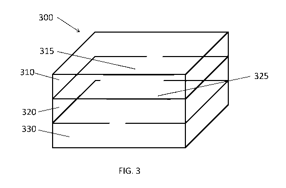
[00108] FIG. 3 is an illustration of a capacitor comprising two integral
material electrodes
sandwiched by dielectric layers, in accordance with certain examples;
[00109] FIG. 4 is an illustration of a capacitor comprising two integral
material electrodes
sandwiched by dielectric layers and dielectric end caps, in accordance with
certain examples;
[00110] FIG. 5 is an illustration of a circuit configured to provide an
output signal, in
accordance with certain embodiments;
[00111] FIG. 6 is an illustration of another circuit configured to provide
an output signal,
in accordance with certain embodiments;
[00112] FIG. 7 is an illustration of a self-shielded capacitor comprising
three integral
material electrodes, in accordance with certain examples;
22
CA 03038465 2019-03-26
WO 2018/060855
PCT/IB2017/055858
[00113] FIG. 8 is an illustration of a self-shielded capacitor comprising
four integral
material electrodes, in accordance with certain examples;
[00114] FIG. 9 is an illustration of a circuit configured to provide a
differential output
signal and which includes the capacitor of FIG. 8, in accordance with certain
configurations;
[00115] FIG. 10 is a block diagram of a mass spectrometer, in accordance
with certain
examples;
[00116] FIG. 11 is a block diagram showing a RF generator electrically
coupled to a mass
analyzer, in accordance with certain embodiments;
[00117] FIG. 12A is an illustration of a hexapole, and FIG. 12B is an
illustration of an
octopole, in accordance with certain embodiments;
[00118] FIGS. 13A-13C are views of an electrode/dielectric layer assembly,
in
accordance with certain embodiments;
[00119] FIG. 14 is an illustration of an integral material electrode
comprising apertures, in
accordance with certain examples; and
[00120] FIG. 15 is a photograph of a self-shielded four electrode
capacitor, in accordance
with certain configurations.
[00121] It will be recognized by the person of ordinary skill in the art
that the features
shown in the figures are not necessarily shown to scale and are illustrated to
facilitate a better
understanding of the technology described herein.
[00122] DETAILED DESCRIPTION
[00123] Certain configurations described herein are directed to capacitors
and circuits
including them which can be used in radio frequency generators that are
electrically coupled to
some component of a mass filter. For example, the capacitor may be present in
a feedback
circuit of a RF generator configured to provide one or more RF signals to one
or more poles of a
multi-pole mass filter designed to select or guide ions in an ion beam.
[00124] While various electrode configurations are described below as
having electrodes
separated by a dielectric medium or layer, if desired, coplanar electrodes can
be present where
more than a single electrode is sandwiched between two dielectric layers. For
example, two
electrodes may be present in a common dielectric layer with some dielectric
medium separating
the two coplanar electrodes. Coplanar electrodes can still provide a capacitor
as described
herein as the electric field between the coplanar electrodes can be coupled by
the surrounding
dielectric material. If desired, more than two coplanar electrodes can be
present in any single
23
CA 03038465 2019-03-26
WO 2018/060855
PCT/IB2017/055858
dielectric layer with some dielectric medium of the same layer separating the
electrodes in that
dielectric layer.
[00125] In certain examples and referring to FIG. 1, a mass filter 100 may
comprise a
plurality of poles, which in this configuration is shown as a quadrupole with
four separate poles
or rods 112, 114, 116 and 118. Oscillating RF voltages from a RF generator are
typically
applied to each of the rods 112, 114, 116 and 118 in a selected amount to
select or filter out ions
with a specific m/z ratio. The filtered ions traverse through the central
opening 125 of the
quadrupole and are provided to a downstream detector (not shown) for detection
or to another
component downstream of the mass filter. The RF voltages can be changed to
detect ions with a
different m/z ratio as desired. A negative feedback loop can be implemented to
generate
controlled, stable electrical signals. When the loop gain of the feedback is
sufficiently large, the
stability of the signals from the RF generator can be governed by the
stability of the passive
components, such as the capacitors of the RF generator. In ceramic capacitors,
however,
temperature stability is typically limited to 15 ppmfC to 30 ppmfC, with these
coefficients of
thermal expansion being determined, for example, by ASTM E831 dated 2000 and
entitled
"Standard Test Method for Linear Thermal Expansion of Solid Materials by
Thermomechanical
Analysis." Reference below and in the appended claims to materials having a
certain coefficient
of thermal expansion (CTE) is based on the CTE as tested by ASTM E831 dated
2000 unless
otherwise noted. For ceramic capacitors, temperature changes of 10 C or more
can cause
unstable RF signals to be generated. Further, ceramic capacitors tend to be
unshielded, which
adds additional unwanted noise to the RF signals.
[00126] In certain embodiments, to overcome the instability of ceramic
capacitors, thin-
film capacitors have been implemented in many circuits. Bonding of the thin
films to substrates
reduces the CTE of the thin film materials. However, production of thin film
capacitors is costly
and complex. Thin film capacitors are also typically unshielded, and mounting
of thin film
capacitors to printed circuit boards can be difficult without shoring the
bottom electrode of the
thin film capacitor. Further, CTE mismatch in the thin film materials and the
other components
of the capacitor can increase instability with increasing temperatures.
[00127] In some examples, integral materials electrodes with a low
coefficient of thermal
expansion can be used in the capacitors described herein. The term "integral
material" refers to
the electrode not including any thin films and generally being produced from
solid materials,
through in certain configurations, the electrode materials may be layered
integral materials to
increase the overall thickness of the electrodes. Referring to FIG. 2, a side
view of a capacitor
200 is shown. The capacitor 200 comprises a first electrode 210 and a second
electrode 220
spatially separated from the first electrode 210 through a dielectric material
or medium 230. As
24
CA 03038465 2019-03-26
WO 2018/060855
PCT/IB2017/055858
noted in more detail below, each of the electrodes 210, 220 may comprise a low
CTE material,
e.g., one with a CTE less than 15 ppmfC, or less than 10 ppmfC or even less
than 5 ppmfC,
3ppmfC or 1 ppmfC such that little or no expansion of the electrodes 210, 220
occurs over a
selected temperature range. Similarly, the dielectric material 230 may
comprise a low CTE
material, which may comprise about the same CTE as the materials of the
electrodes 210, 220 so
if any expansion occurs with increasing temperature then all of the materials
expand at about the
same rate. While not shown in FIG. 2, the electrodes 210, 220 typically
comprise a site at one
side or surface of the capacitor 200 to permit electrical coupling of the
capacitor 200 to a circuit
which may be part of an RF generator circuit or other electrical circuit. In
the configuration of
FIG. 2, the electrodes 210, 220 "float" within the dielectric material 230 and
are not generally
coupled to the dielectric material 230 using any adhesive or other material.
In producing the
capacitor 200, the electrodes 210, 220 can be held in a jig or mold in a fixed
position from each
other, and the dielectric material 230 can be poured, 3D-printed, or otherwise
disposed into the
mold at high temperature and permitted to solidify. Solidification (or curing)
of the dielectric
material 230 holds the electrodes 210, 220 in place without the need to use
any adhesive or other
materials to produce the capacitor 200. The entire block of the electrodes
210, 220 and
dielectric material 230 can then be removed from the mold to provide the
capacitor. If desired,
channels or pathways can be drilled or produced in the dielectric material 230
to permit
electrical coupling of each of the electrodes 210, 220 to the RF generator
circuit. In other
instances, slots can be machined into the dielectric medium 230, and the
electrodes 210, 220 can
be inserted into the slots and fixed in position by disposing additional
dielectric medium around
the inserted electrodes 210, 220 to seal any open space and fix the electrodes
210, 220 into
position. The additional dielectric medium can be the same or different from
the dielectric
medium 230. By producing the capacitor 200 using integral material electrodes
210, 220 which
are trapped within the dielectric medium 230, a more stable capacitor can be
provided. As noted
in more detail below, the electrodes 210, 220 can be sized and shaped to be
the same or different
and may comprise holes, apertures or other features to reduce the overall
weight and/or the
amount of material needed.
[00128] In certain examples, the materials used in the electrodes 210, 220
typically
comprise a coefficient of thermal expansion of less than 15 ppmiC as tested by
ASTM E831
dated 2000. While the exact CTE of the integral materials of the electrodes
can vary, in some
instances it may be desirable to select low CTE materials, e.g., those having
a CTE of 5 ppmfC
or less to increase overall stability of the capacitor with changing
temperature. Illustrative
materials for use in the electrodes 210, 220 include, but are not limited to,
nickel iron alloys with
a CTE of 15 ppmfC of less, e.g., Invar alloys such as, for example, Invar 36,
Super Invar, 52
CA 03038465 2019-03-26
WO 2018/060855
PCT/IB2017/055858
Alloy, 48 Alloy, 46 Alloy, 42 Alloy, 42-6 Alloy, and the like. In other
configurations, the
integral material electrodes may comprise a zinc alloy with a CTE of 15 ppmfC
or less. In
some instances, the integral material electrodes may comprise a chromium
nickel iron super
alloy with a CTE of 15 ppmfC or less. In additional instances, the integral
material electrodes
may comprise iron cobalt nickel alloys with a CTE of 15 ppmfC or less, e.g.,
Kovar alloys. In
other configurations, the integral material electrodes may comprise iron
cobalt nickel aluminum
titanium niobium alloys with a CTE of 15 ppmfC or less. While the exact useful
temperature
range of the integral materials of the electrodes can vary, the integral
materials used in the
electrodes typically comprise a CTE of 15 ppmfC or less over a temperature
range of about 30
C to about 900 C. In some instances, the material used in the integral
material electrodes
comprises a CTE of 10 ppmfC or less over a temperature range of about 30 C to
about 500 C.
In other instances, the material used in the integral material electrodes
comprises a CTE of about
ppmfC or less over a temperature range of about 30 C to about 300 C. In
additional
configurations, the material used in the integral material electrodes
comprises a CTE of about 2
ppmf C or less over a temperature range of about 30 C to about 200 C. The
materials used in
the integral material electrodes 210, 220 can be the same or can be different.
Further, the exact
thickness and spacing of the electrodes 210, 220 can vary.
[00129] In some examples, illustrative materials for use as the dielectric
medium 230
include, but are not limited to, low CTE quartz, e.g., quartz with a CTE of 15
ppmfC or less,
metal oxides with a CTE of 15 ppmiC or less, glasses with a CTE of 15 ppmfC or
less,
semiconductors with a CTE of 15 ppmfC or less, sapphire based materials with a
CTE of 15
ppmf C or less, diamond based materials with a CTE of 15 ppmfC or less. In
some instances,
the dielectric medium may be a single component dielectric medium with a
generally
homogeneous dielectric material being present. In other instances, a dopant or
additive may be
present in the dielectric medium to alter the overall properties of the
dielectric medium. In a
typical configuration, the dielectric medium is non-conductive and generally
does not distort or
otherwise interfere with (to a substantial degree) the functioning, e.g., the
electric fields, of the
integral material electrodes. Where a liquid dielectric medium is added to a
mold comprising
the electrodes 210, 220, the liquid dielectric medium is selected so the
melting point of the
liquid dielectric medium is at least 50 C less, at least 100 C less or at
least 150 C less than the
melting point of the integral electrodes 210, 220 to prevent the electrodes
210, 220 from
becoming liquid during production. In final form, the dielectric medium is
desirably solid over
the operating temperature range of the capacitor. In some instances, the
dielectric layer 230 may
be produced by stacking a plurality of separate dielectric layers on each
other to provide a
desired overall thickness.
26
CA 03038465 2019-03-26
WO 2018/060855
PCT/IB2017/055858
[00130] In certain configurations, the capacitors described herein can also
be produced by
sandwiching two or more electrodes between individual dielectric layers.
Referring to FIG. 3, a
capacitor 300 is shown that comprises dielectric layers 310, 320 and 330. A
first electrode 315
is positioned between the dielectric layers 310, 320, and a second electrode
325 is positioned
between the dielectric layers 320, 330. Unlike most capacitors where the
electrodes are strongly
bonded to the dielectric media, in the configuration of FIG. 3, the electrodes
315, 325 are not
glued or epoxied to the layers 310, 320 and 330. The electric field of the
signal is mostly
confined within the region between the electrodes 315, 325. In certain
instances, that region is
entirely free of foreign material (e.g., epoxy) so that only low CTE materials
and perhaps a small
amount of air are present in that region. By omitting epoxy or other adhesive
materials in the
region between the electrodes 315, 325, the capacitor is more stable with
changes in
temperature. For example, since the electrodes 315, 325 near the electric
field of interest are not
bonded to the layers 310, 320 and 330, the electrodes and dielectric layers
are free to expand or
contract independently with changing temperature. Any potential issue of
cracking at the
electrode/dielectric layer interface is minimized or eliminated.
[00131] In certain configurations, in producing the sandwiched capacitor
shown in FIG. 3,
the electrodes 315, 325 are each mechanically held against the dielectric
layer 320, the dielectric
layer 310 is added to the top of electrode 315, and the dielectric layer 330
is added to the bottom
of the electrode 325. The entire construct is pressed together and can be held
in place using, for
example, low CTE adhesive or epoxy at the edges of the layers 310, 320 and
330. Alternatively,
the dielectric layers 310, 320 and 330 can be fixed in place using mechanical
fasteners such as
screws or brackets without the need to use any epoxy or adhesive. In another
configuration, the
electrodes 315, 325 can be glued/epoxied at the terminals (outside the
electric field of interest)
to the dielectric layers 310, 320 and 330. Epoxy between the substrate gaps
near the edges
should not substantially affect the overall stability, because the epoxy is a
relatively thin layer
compared to the full thickness of the substrate and it is outside of the
electric field of interest. If
desired, the epoxy may be selected so that its CTE is about the same as the
dielectric layers. In
another configuration, the epoxy can be applied only to the outer edges of the
dielectric
substrates with the gaps between the dielectric substrates are free of epoxy
and generally
occupied by air space present from the electrodes 315, 325 being sandwiched
between the layers
310, 320 and 330. In an alternative configuration, epoxy can be applied to the
electrodes 315,
325 outer surfaces to fix electrode 315 to layer 310 and electrode 325 to
layer 330. Epoxy is
typically not present between the electrode 315 and the layer 320 or the
electrode 325 and the
layer 320 as the electric field of interest is present in the layer 320.
27
CA 03038465 2019-03-26
WO 2018/060855
PCT/IB2017/055858
[00132] In certain examples, the materials used in the electrodes 315, 325
typically
comprise a coefficient of thermal expansion of less than 15 ppmiC as tested by
ASTM E831
dated 2000. While the exact CTE of the integral materials of the electrodes
can vary, in some
instances it may be desirable to select low CTE materials, e.g., those having
a CTE of 5 ppmPC
or less to increase overall stability of the capacitor with changing
temperature. Illustrative
materials for use in the electrodes 315, 325 include, but are not limited to,
nickel iron alloys with
a CTE of 15 ppmPC of less, e.g., Invar alloys such as, for example, Invar 36,
Super Invar, 52
Alloy, 48 Alloy, 46 Alloy, 42 Alloy, 42-6 Alloy, and the like. In other
configurations, the
integral material electrodes 315, 325 may comprise a zinc alloy with a CTE of
15 ppmiC or
less. In some instances, the integral material electrodes 315, 325 may
comprise a chromium
nickel iron super alloy with a CTE of 15 ppmPC or less. In additional
instances, the integral
material electrodes 315, 325 may comprise iron cobalt nickel alloys with a CTE
of 15 ppmPC or
less, e.g. Kovar alloys. In other configurations, the integral material
electrodes 315, 325 may
comprise iron cobalt nickel aluminum titanium niobium alloys with a CTE of 15
ppmPC or less.
While the exact useful temperature range of the integral materials 315, 325 of
the electrodes can
vary, the integral materials used in the electrodes 315, 325 typically
comprise a CTE of 15
ppmPC or less over a temperature range of about 30 C to about 900 C. In some
instances, the
material used in the integral material electrodes 315, 325 comprises a CTE of
10 ppmPC or less
over a temperature range of about 30 C to about 500 C. In other instances,
the material used in
the integral material electrodes 315, 325 comprises a CTE of about 5 ppmPC or
less over a
temperature range of about 30 C to about 300 C. In additional
configurations, the material
used in the integral material electrodes 315, 325 comprises a CTE of about 2
ppmPC or less
over a temperature range of about 30 C to about 200 C. The materials used in
the integral
material electrodes 315, 325 can be the same or can be different. Further, the
exact thickness
and spacing of the electrodes 315, 325 can vary.
[00133] In some examples, illustrative materials for use as the dielectric
medium of the
layers 310, 320 and 330 include, but are not limited to, low CTE quartz, e.g.,
quartz with a CTE
of 15 ppmiC or less, metal oxides with a CTE of 15 ppmPC or less, glasses with
a CTE of 15
ppmPC or less, semiconductors with a CTE of 15 ppmiC or less, sapphire based
materials with
a CTE of 15 ppmPC or less, diamond based materials with a CTE of 15 ppmiC or
less. In some
instances, the dielectric medium in each of the layers 310, 320, 330 may be a
single component
dielectric medium with a generally homogeneous dielectric material being
present. In other
instances, a dopant or additive may be present in one or more of the layers
310, 320, 330 to alter
the overall properties of the dielectric medium. In a typical configuration,
the dielectric medium
is non-conductive and generally does not distort or otherwise interfere with
(to a substantial
28
CA 03038465 2019-03-26
WO 2018/060855
PCT/IB2017/055858
degree) the functioning, e.g., the electric fields, of the integral material
electrodes. Where a
liquid dielectric medium is added to a mold comprising the electrodes 315,
325, the liquid
dielectric medium is selected so the melting point of the liquid dielectric
medium is at least 50
C less, at least 100 C less or at least 150 C less than the melting point of
the integral
electrodes 315, 325 to prevent the electrodes 315, 325 from becoming liquid
during production.
In final form, the dielectric medium is desirably solid over the operating
temperature range of
the capacitor. The dielectric layers 310, 320 and 330 need not all have the
same dielectric
material or composition or the same thickness or shape. For example, one or
more of the
dielectric layers 310, 320 and 330 may be produced by stacking a plurality of
separate dielectric
layers on each other to provide a desired overall thickness.
[00134] In certain examples and referring to FIG. 4, another configuration
of a capacitor
is shown. The capacitor 400 comprises electrodes 415, 425, dielectric layers
410, 420 and 430
and dielectric end caps 440 and 450. The electrode 415 is positioned between
the dielectric
layers 410, 420, and the electrode 425 is positioned between the dielectric
layers 420, 430. The
electrodes 415, 425 are not glued or epoxied to the layers 410, 420 and 430.
The electric field of
the signal is mostly confined within the region between the electrodes 415,
425. In certain
instances, that region is entirely free of foreign material (e.g., epoxy) so
that only low CTE
materials and perhaps a small amount of air is present in that region. By
omitting epoxy or other
adhesive in the region between the electrodes 415, 425, the capacitor is more
stable. For
example, since the electrodes 415, 425 near the electric field of interest are
not bonded to the
layers 410, 420 and 430, the electrodes and dielectric layers are free to
expand or contract
independently with changing temperature. Any potential issue of cracking at
the
electrode/dielectric layer interface is minimized or eliminated. Further, the
end caps 440, 450
can be epoxied or glued at the sides to each of the dielectric layers 410, 420
and 430 so that no
epoxy or adhesive is present in the body of the capacitor 400. The end caps
440, 450 may also
comprise a low CTE material, which can further enhance stability since the
epoxy or adhesive's
coefficient of thermal expansion will be overcome by the low CTE of the end
caps 440, 450.
The dimensions and small gaps between the layers 410, 420 and 430 can be fixed
by coupling
the layers to the end caps 440, 450.
[00135] In certain examples, in producing the sandwiched capacitor shown in
FIG. 4, the
electrodes 415, 425 are each mechanically held against the dielectric layer
420, the dielectric
layer 410 is added to the top of electrode 415, and the dielectric layer 430
is added to the bottom
of the electrode 425. The entire assembly is pressed together. The end caps
440 and 450 are
then adhered to each of the layers 410, 420 and 430 at the edges of these
layers using an epoxy
or adhesive. For example, a low CTE adhesive or epoxy, e.g., one with a CTE of
15 ppmiC or
29
CA 03038465 2019-03-26
WO 2018/060855
PCT/IB2017/055858
less, can be added at the outer edges of the layers 410, 420 and 430, and the
end caps 440, 450
may then be placed at the sides of the layers 410, 420 and 430 to fix the
position of the
electrodes 415, 425 and the layers 410, 420 and 430. Alternatively, the end
caps 440, 450 can
be held to the dielectric layers 410, 420 and 430 using mechanical fasteners
such as screws or
brackets without the need to use any epoxy or adhesive. In another
configuration, the epoxy can
be applied to the outer edges of the dielectric layers 410, 420, 430 and to
the outer surfaces of
the layers 410, 420, 430 so multiple different epoxy sites are present to hold
the layers 410, 420
and 430 in place. In an alternative configuration, epoxy can also be applied
to the electrodes
415, 425 outer surfaces to fix electrode 415 to layer 410 and electrode 425 to
layer 430. Epoxy
is typically not present between the electrode 415 and the layer 420 or the
electrode 425 and the
layer 420 as the electric field of interest is present in the layer 420.
[00136] In certain examples, the materials used in the electrodes 415, 425
typically
comprise a coefficient of thermal expansion of less than 15 ppmiC as tested by
ASTM E831
dated 2000. While the exact CTE of the integral materials of the electrodes
can vary, in some
instances it may be desirable to select low CTE materials, e.g., those having
a CTE of 5 ppmfC
or less to increase overall stability of the capacitor with changing
temperature. Illustrative
materials for use in the electrodes 415, 425 include, but are not limited to,
nickel iron alloys with
a CTE of 15 ppmfC of less, e.g., Invar alloys such as, for example, Invar 36,
Super Invar, 52
Alloy, 48 Alloy, 46 Alloy, 42 Alloy, 42-6 Alloy, and the like. In other
configurations, the
integral material electrodes 415, 425 may comprise a zinc alloy with a CTE of
15 ppmiC or
less. In some instances, the integral material electrodes 415, 425 may
comprise a chromium
nickel iron super alloy with a CTE of 15 ppmf C or less. In additional
instances, the integral
material electrodes 415, 425 may comprise iron cobalt nickel alloys with a CTE
of 15 ppmfC or
less, e.g. Kovar alloys. In other configurations, the integral material
electrodes 415, 425 may
comprise iron cobalt nickel aluminum titanium niobium alloys with a CTE of 15
ppmfC or less.
While the exact useful temperature range of the integral materials 415, 425 of
the electrodes can
vary, the integral materials used in the electrodes 415, 425 typically
comprise a CTE of 15
ppmf C or less over a temperature range of about 30 C to about 900 C. In
some instances, the
material used in the integral material electrodes 415, 425 comprises a CTE of
10 ppmfC or less
over a temperature range of about 30 C to about 500 C. In other instances,
the material used in
the integral material electrodes 415, 425 comprises a CTE of about 5 ppmfC or
less over a
temperature range of about 30 C to about 300 C. In additional
configurations, the material
used in the integral material electrodes 415, 425 comprises a CTE of about 2
ppm/C or less
over a temperature range of about 30 C to about 200 C. The materials used in
the integral
CA 03038465 2019-03-26
WO 2018/060855
PCT/IB2017/055858
material electrodes 415, 425 can be the same or can be different. Further, the
exact thickness
and spacing of the electrodes 415, 425 can vary.
[00137] In some examples, illustrative materials for use as the dielectric
medium of the
layers 410, 420 and 430 and the end caps 440, 450 include, but are not limited
to, low CTE
quartz, e.g., quartz with a CTE of 15 ppmfC or less, metal oxides with a CTE
of 15 ppmfC or
less, glasses with a CTE of 15 ppmiC or less, semiconductors with a CTE of 15
ppmfC or less,
sapphire based materials with a CTE of 15 ppmfC or less, diamond based
materials with a CTE
of 15 ppmiC or less. In some instances, the dielectric medium in each of the
layers 410, 420,
430 and the end caps 440, 450 may be a single component dielectric medium with
a generally
homogeneous dielectric material being present. In other instances, a dopant or
additive may be
present in one or more of the layers 410, 420, 430 and/or the end caps 440,
450 to alter the
overall properties of the dielectric medium. In a typical configuration, the
dielectric medium is
non-conductive and generally does not distort or otherwise interfere with (to
a substantial
degree) the functioning, e.g., the electric fields, of the integral material
electrodes. Where a
liquid dielectric medium is added to a mold comprising the electrodes 415,
425, the liquid
dielectric medium is selected so the melting point of the liquid dielectric
medium is at least 50
C less, at least 100 C less or at least 150 C less than the melting point of
the integral
electrodes 415, 425 to prevent the electrodes 415, 425 from becoming liquid
during production.
In final form, the dielectric medium is desirably solid over the operating
temperature range of
the capacitor. The dielectric layers 410, 420 and 430 need not all have the
same dielectric
material or composition or the same thickness or shape. For example, one or
more of the
dielectric layers 410, 420 and 430 may be produced by stacking a plurality of
separate dielectric
layers on each other to provide a desired overall thickness. Similarly, the
end caps 440, 450
may comprise a different dielectric medium from the layers 410, 420, 430
and/or a different
thickness and/or shape. For example, if desired, the end caps may take the
form of thin strips of
material which can be adhered to the sides of the layers 410, 420 and 430 to
fix those layers into
position. In other instances, the end caps 440, 450 can be configured as
generally L-shaped
members which can engage two or more different surfaces of the capacitor 400
to fix the layers
410, 420 and 430 into position. If desired, one or both of the end caps 440,
450 may comprise a
plurality of individual layers which are stacked together to provide an
overall desired thickness.
[00138] In certain instances, it may be desirable to shield some portion of
the capacitor to
prevent the RF signals from being affected by any external parasitic
capacitive coupling. An
illustration how parasitic capacitive coupling may arise is shown using the
circuit 500 of FIG. 5
as one example. An intended signal 505, or intended amplitude set point of a
signal, is shown as
being provided to the circuit 500 comprising a difference amplifier, or a
passive signal summer
31
CA 03038465 2019-03-26
WO 2018/060855
PCT/IB2017/055858
where the feedback is inverted and added to the intended signal 510, an
amplifier 520, a
feedback network 530 and an output feedback capacitor 540. Undesirable
external noise 545
and/or parasitic capacitive coupling 535 from external components, e.g., a
grounded metal
housing, can add noise to the signal 525 provided to the capacitor 540, which
generally cannot
be corrected using the feedback loop of the circuit 500. For example,
capacitors are often used
as part of a feedback network to sample an RF output signal stabilized by a
negative feedback
loop, e.g., a high voltage RF generator configured to drive a quadrupole mass
filter in a mass
spectrometry instrument. Despite the use of a stable capacitor in a negative
feedback loop, the
stability or integrity of the output signal 555 is degraded if there is
unstable parasitic capacitive
coupling 535 to components adjacent to the capacitor or if EMI noise 545 is
radiated from other
components. This kind of signal error cannot be corrected by the feedback loop
and provides an
unstable feedback signal 515 and a resulting unstable output signal 555.
[00139] In certain configurations, the capacitors described herein may be
self-shielded so
that the feedback signals from the capacitor are not substantially affected by
external noise or
unstable parasitic capacitive coupling. Referring to the circuit 600 shown in
FIG. 6, an intended
signal 605, or intended amplitude set point of a signal, is shown as being
provided to the circuit
600 comprising a difference amplifier, or a passive signal summer where the
feedback is
inverted and added to the intended signal 610, an amplifier 620, a feedback
network 630 and a
shielded output feedback capacitor 640. Undesirable external noise 645 and/or
parasitic
capacitive coupling 635 from external components do not add noise to the
output signal 655
since the capacitor 640 is self-shielded. Due to the high gain of the feedback
loop, the output
655 is stabilized by the feedback loop with a low output impedance. The output
signal 655 and
the other signals 605, 615 and 625 are unaffected by external parasitic
coupling. Noise injected
to the output will also be generally be suppressed, e.g., when the noise is at
a lower frequency
than the feedback loop response time. The self-shielding nature of the
capacitor can be used to
shield the other electrodes with a sensitive feedback signal from external
noise or unstable
parasitic coupling. As noted below, the self-shielding can be implemented in
combination with
the integral material electrodes or, if desired, self-shielding can be
implemented with other types
of electrodes, e.g., thin film electrodes or ceramic electrodes if desired.
[00140] In certain examples and referring to FIG. 7, one illustration of a
self-shielded
capacitor 700 is shown. The self-shielded capacitor 700 comprises electrodes
715, 725 and 735
positioned within or between dielectric layers 710, 720, 730, and 740.
Electrode 715 is between
layers, 710, 720. Electrode 725 is between layers 720, 730. Electrode 735 is
between layers
730, 740. The electrodes 715, 725 are each mechanically held against the
dielectric layer 720,
the dielectric layer 710 is added to the top of electrode 715, and the
dielectric layer 730 is added
32
CA 03038465 2019-03-26
WO 2018/060855
PCT/IB2017/055858
to the bottom of the electrode 725. The electrode 735 can then be held against
the dielectric
layer 730, and the dielectric layer 740 can be coupled to the electrode 735.
The entire construct
is pressed together and can be held in place using, for example, low CTE
adhesive or epoxy at
the edges of the layers 710, 720, 730 and 740. If desired, end caps (not
shown) similar to those
of FIG. 4 can be coupled to the layers 710, 720, 730 and 740. Alternatively,
the dielectric layers
710, 720, 730 and 740 can be fixed in place using mechanical fasteners such as
screws or
brackets without the need to use any epoxy or adhesive. In another
configuration, the electrodes
715, 725 and 735 can be glued/epoxied at the terminals (outside the electric
field of interest) to
the dielectric layers 710, 720, 730 and 740. Epoxy between the substrate gaps
near the edges
should not substantially affect the overall stability, because the epoxy is a
relatively thin layer
compared to the full thickness of the substrate and it is outside of the
electric field of interest. If
desired, the epoxy may be selected so that its CTE is about the same as the
dielectric layers. In
another configuration, the epoxy can be applied only to the outer edges of the
dielectric
substrates with the gaps between the dielectric substrates (which are free of
epoxy and generally
occupied by air space) present from the electrodes 715, 725 and 735 being
sandwiched between
the layers 710, 720, 730 and 740. In an alternative configuration, epoxy can
be applied to the
electrodes 715, 725, 735 outer surfaces to fix electrode 715 to layer 710, and
to fix the electrode
735 to layer 740. Epoxy is typically not present between the electrodes 715,
725 and 735. In
use of the capacitor 700, the electrodes 715 and 735 can be electrically
connected to each other
and used to provide the output signal. As noted in connection with FIG. 6, the
output signal is
stabilized by a negative feedback loop. Electrodes 715, 735 act to shield the
electrode 725,
which is carrying the sensitive feedback signal. Shielding of the electrode
725 by the electrodes
715, 735 prevents introduction of external noise or perturbations into the
feedback signal and
provides a more stable output signal.
[00141] In certain examples, the materials used in the electrodes 715, 725,
735 typically
comprise a coefficient of thermal expansion of less than 15 ppmiC as tested by
ASTM E831
dated 2000. While the exact CTE of the integral materials of the electrodes
can vary, in some
instances it may be desirable to select low CTE materials, e.g., those having
a CTE of 5 ppmfC
or less to increase overall stability of the capacitor with changing
temperature. Illustrative
materials for use in the electrodes 715, 725, 735 include, but are not limited
to, nickel iron alloys
with a CTE of 15 ppmfC of less, e.g., Invar alloys such as, for example,
Invar 36, Super Invar,
52 Alloy, 48 Alloy, 46 Alloy, 42 Alloy, 42-6 Alloy and the like. In other
configurations, the
integral material electrodes 715, 725, 735 may comprise a zinc alloy with a
CTE of 15 ppmiC
or less. In some instances, the integral material electrodes 715, 725, 735 may
comprise a
chromium nickel iron super alloy with a CTE of 15 ppmfC or less. In additional
instances, the
33
CA 03038465 2019-03-26
WO 2018/060855
PCT/IB2017/055858
integral material electrodes 715, 725, 735 may comprise iron cobalt nickel
alloys with a CTE of
15 ppmfC or less, e.g. Kovar alloys. In other configurations, the integral
material electrodes
715, 725, 735 may comprise iron cobalt nickel aluminum titanium niobium alloys
with a CTE of
15 ppmiC or less. While the exact useful temperature range of the integral
materials 715, 725,
735 of the electrodes can vary, the integral materials used in the electrodes
715, 725, 735
typically comprise a CTE of 15 ppmfC or less over a temperature range of about
30 C to about
900 C. In some instances, the material used in the integral material
electrodes 715, 725, 735
comprises a CTE of 10 ppmfC or less over a temperature range of about 30 C to
about 500 C.
In other instances, the material used in the integral material electrodes 715,
725, 735 comprises a
CTE of about 5 ppmfC or less over a temperature range of about 30 C to about
300 C. In
additional configurations, the material used in the integral material
electrodes 715, 725, 735
comprises a CTE of about 2 ppmfC or less over a temperature range of about 30
C to about
200 C. The materials used in the integral material electrodes 715, 725, 735
can be the same or
can be different. Further, the exact thickness and spacing of the electrodes
715, 725, and 735
can vary, and the spacing between electrodes 715 and 725 need not be the same
as the spacing
between electrodes 725 and 735.
[00142] In some examples, illustrative materials for use as the dielectric
medium of the
layers 710, 720, 730 and 740 include, but are not limited to, low CTE quartz,
e.g., quartz with a
CTE of 15 ppmfC or less, metal oxides with a CTE of 15 ppmfC or less, glasses
with a CTE of
15 ppmfC or less, semiconductors with a CTE of 15 ppmfC or less, sapphire
based materials
with a CTE of 15 ppmiC or less, diamond based materials with a CTE of 15 ppmiC
or less. In
some instances, the dielectric medium in each of the layers 710, 720, 730 and
740 may be a
single component dielectric medium with a generally homogeneous dielectric
material being
present. In other instances, a dopant or additive may be present in one or
more of the layers 710,
720, 730 and 740 to alter the overall properties of the dielectric medium. In
a typical
configuration, the dielectric medium is non-conductive and generally does not
distort or
otherwise interfere with (to a substantial degree) the functioning, e.g., the
electric fields, of the
integral material electrodes. Where a liquid dielectric medium is added to a
mold comprising
the electrodes 715, 725, 735, the liquid dielectric medium is selected so the
melting point of the
liquid dielectric medium is at least 50 C less, at least 100 C less or at
least 150 C less than the
melting point of the integral electrodes 715, 725, 735 to prevent the
electrodes 715, 725, 735
from becoming liquid during production. In final form, the dielectric medium
is desirably solid
over the operating temperature range of the capacitor. The dielectric layers
710, 720, 730 and
740 need not all have the same dielectric material or composition or the same
thickness or shape.
In some instances, one or more of the dielectric layers 710, 720, 730, 740 may
be produced by
34
CA 03038465 2019-03-26
WO 2018/060855
PCT/IB2017/055858
stacking a plurality of separate dielectric layers on each other to provide a
desired overall
thickness.
[00143] While the configurations described above in connection with FIGS.
2, 3-4 and 7
include two or three electrodes, it may be desirable to include four, five or
more separate
electrodes in the capacitors described herein. In particular, where self-
shielded capacitors are
used, the presence of four or more electrodes may provide certain desirable
attributes including
highly stable output signals.
[00144] In certain configurations and referring to FIG. 8, a four electrode
capacitor 800 is
shown. The capacitor comprises electrodes 815, 825, 835 and 845 and dielectric
layers 810,
820, 830, 840 and 850. Electrode 815 is sandwiched between the layers 810,
820, electrode 825
is sandwiched between the layers 820, 830, electrode 835 is sandwiched between
layers 830,
840 and electrode 845 is sandwiched between layers 840, 850. The electrodes
815, 825 are each
mechanically held against the dielectric layer 820, the dielectric layer 810
is added to the top of
electrode 815, and the dielectric layer 830 is added to the bottom of the
electrode 825. The
electrode 835 can then be held against the dielectric layer 830, and the
dielectric layer 840 can
be coupled to the electrode 835. The electrode 845 can then be held against
the dielectric layer
840, and the dielectric layer 850 can be coupled to the electrode 845. The
entire construct is
pressed together and can be held in place using, for example, low CTE adhesive
or epoxy at the
edges of the layers 810, 820, 830, 840 and 850. If desired, end caps (not
shown) similar to those
of FIG. 4 can be coupled to the layers 810, 820, 830, 840 and 850.
Alternatively, the dielectric
layers 810, 820, 830, 840 and 850 can be fixed in place using mechanical
fasteners such as
screws or brackets without the need to use any epoxy or adhesive. In another
configuration, the
electrodes 815, 825, 835 and 845 can be glued/epoxied at the terminals
(outside the electric field
of interest) to the dielectric layers 810, 820, 830, 840 and 850. Epoxy
between the substrate gaps
near the edges should not substantially affect the overall stability, because
the epoxy is a
relatively thin layer compared to the full thickness of the substrate and it
outside of the electric
field of interest. If desired, the epoxy may be selected so that its CTE is
about the same as the
dielectric layers. In another configuration, the epoxy can be applied only to
the outer edges of
the dielectric substrates with the gaps between the dielectric substrates are
free of epoxy and
generally occupied by air space present from the electrodes 815, 825, 835 and
845 being
sandwiched between the layers 810, 820, 830, 840 and 850. In an alternative
configuration,
epoxy can be applied to the electrodes 815, 845 outer surfaces to fix
electrode 815 to layer 810,
and to fix electrode 845 to the layer 850. Epoxy is typically not present
between the electrodes
815, 825, 835 and 845. In use of the capacitor 800, electrodes 815 and 845 can
be configured to
carry the differential output signals, which are stabilized by a negative
feedback loop, as
CA 03038465 2019-03-26
WO 2018/060855
PCT/IB2017/055858
discussed in more detail in connection with FIG. 9. Electrodes 815, 845 also
shield electrodes
825, 835, which carry the sensitive differential feedback signals. Shielding
of the electrodes
825, 835 by the electrodes 815, 845 prevents introduction of external noise or
perturbations into
the feedback signal and provides a more stable output signal.
[00145] In certain examples, the materials used in the electrodes 815, 825,
835 and 845
typically comprise a coefficient of thermal expansion of less than 15 ppmiC as
tested by ASTM
E831 dated 2000. While the exact CTE of the integral materials of the
electrodes can vary, in
some instances it may be desirable to select low CTE materials, e.g., those
having a CTE of 5
ppmfC or less to increase overall stability of the capacitor with changing
temperature.
Illustrative materials for use in the electrodes 815, 825, 835 and 845
include, but are not limited
to, nickel iron alloys with a CTE of 15 ppmfC of less, e.g., Invar alloys
such as, for example,
Invar 36, Super Invar, 52 Alloy, 48 Alloy, 46 Alloy, 42 Alloy, 42-6 Alloy and
the like. In other
configurations, the integral material electrodes 815, 825, 835, 845 may
comprise a zinc alloy
with a CTE of 15 ppmfC or less. In some instances, the integral material
electrodes 815, 825,
835, 845 may comprise a chromium nickel iron super alloy with a CTE of 15
ppmfC or less. In
additional instances, the integral material electrodes 815, 825, 835, 845 may
comprise iron
cobalt nickel alloys with a CTE of 15 ppmfC or less, e.g. Kovar alloys. In
other configurations,
the integral material electrodes 815, 825, 835, 845 may comprise iron cobalt
nickel aluminum
titanium niobium alloys with a CTE of 15 ppmfC or less. While the exact useful
temperature
range of the integral materials 815, 825, 835, 845 of the electrodes can vary,
the integral
materials used in the electrodes 815, 825, 835, 845 typically comprise a CTE
of 15 ppmiC or
less over a temperature range of about 30 C to about 900 C. In some
instances, the material
used in the integral material electrodes 815, 825, 835, 845 comprises a CTE of
10 ppmfC or
less over a temperature range of about 30 C to about 500 C. In other
instances, the material
used in the integral material electrodes 815, 825, 835, 845 comprises a CTE of
about 5 ppmiC
or less over a temperature range of about 30 C to about 300 C. In additional
configurations,
the material used in the integral material electrodes 815, 825, 835, 845
comprises a CTE of
about 2 ppmfC or less over a temperature range of about 30 C to about 200 C.
The materials
used in the integral material electrodes 815, 825, 835, 845 can be the same or
can be different.
Further, the exact thickness and spacing of the electrodes 815, 825, 835, and
845 can vary, and
the spacing between electrodes 815 and 825 need not be the same as the spacing
between
electrodes 835 and 845.
[00146] In some examples, illustrative materials for use as the dielectric
medium of the
layers 810, 820, 830, 840 and 850 include, but are not limited to, low CTE
quartz, e.g., quartz
with a CTE of 15 ppmfC or less, metal oxides with a CTE of 15 ppmfC or less,
glasses with a
36
CA 03038465 2019-03-26
WO 2018/060855
PCT/IB2017/055858
CTE of 15 ppmfC or less, semiconductors with a CTE of 15 ppmfC or less,
sapphire based
materials with a CTE of 15 ppmfC or less, diamond based materials with a CTE
of 15 ppmiC
or less. In some instances, the dielectric medium in each of the layers 810,
820, 830, 840 and
850 may be a single component dielectric medium with a generally homogeneous
dielectric
material being present. In other instances, a dopant or additive may be
present in one or more of
the layers 810, 820, 830, 840 and 850 to alter the overall properties of the
dielectric medium. In
a typical configuration, the dielectric medium is non-conductive and generally
does not distort
or otherwise interfere with (to a substantial degree) the functioning, e.g.,
the electric fields, of
the integral material electrodes. Where a liquid dielectric medium is added to
a mold
comprising the electrodes 815, 825, 835, 845 the liquid dielectric medium is
selected so the
melting point of the liquid dielectric medium is at least 50 C less, at least
100 C less or at least
150 C less than the melting point of the integral electrodes 815, 825, 835,
845 to prevent the
electrodes 815, 825, 835, 845 from becoming liquid during production. In final
form, the
dielectric medium is desirably solid over the operating temperature range of
the capacitor. The
dielectric layers 810, 820, 830, 840 and 850 need not all have the same
dielectric material or
composition or the same thickness or shape. For example, one or more of the
dielectric layers
810, 820, 830, 840 and 850 may be produced by stacking a plurality of separate
dielectric layers
on each other to provide a desired overall thickness.
[00147] In
certain examples, the self-shielded four electrode capacitor can be used to
provide differential output signals as shown in FIG. 9. The capacitor 905 is
electrically coupled
to a differential feedback network 930, difference amplifier, or a passive
signal summer where
the feedback is inverted and added to the intended signal 910, 920, and
amplifiers 940, 950.
Intended differential signals, or intended amplitude set point of differential
signals, 902, 904,
906 and 908-are provided to the circuit 900. The outer electrodes 915, 945 of
the capacitor 905
provide stabilized +/- output signals 962, 964 as a result of shielding the
inner electrodes 925,
935 of the capacitor 905 from undesirable noise 934 and/or parasitic
capacitive coupling 932.
The inner shielded electrodes 925, 935 carry the +/- feedback signals 922, 924
which result in
continued stabilization of the resulting output signals 962, 964 even with
changes in temperature
and expansion of the electrode materials and/or dielectric materials.
[00148] In
certain embodiments, the capacitors described herein may be particularly
desirable for use in mass spectrometry instruments comprising a multipole mass
filter. For
example, the multipole may be configured as a quadrupole, a hexapole (FIG.
12A) or an
octopole (FIG. 12B).
Referring to FIG. 10, several components of a mass spectrometer are
shown. The mass spectrometer comprises an ion source 1010, a mass analyzer
1020, an optional
sample introduction device 1005 fluidically coupled to the ion source, and an
optional detector
37
CA 03038465 2019-03-26
WO 2018/060855
PCT/IB2017/055858
1030 fluidically coupled to the mass analyzer. In some configurations, the
sample introduction
device 1005 may be configured to aerosolize a liquid sample. Illustrative
sample introduction
devices include, but are not limited to, nebulizers, spray chambers, spray
heads and similar
devices. The ion source 1010 may take many forms and typically provides one or
more ions.
Illustrative ion or ionization sources include, but are not limited to,
plasmas (e.g., inductively
coupled plasmas, capacitively coupled plasmas, microwave-induced plasmas,
etc.), arcs, sparks,
drift ion devices, devices that can ionize a sample using gas-phase ionization
(e.g., electron
ionization, chemical ionization, desorption chemical ionization, negative-ion
chemical
ionization), field desorption devices, field ionization devices, fast atom
bombardment devices,
secondary ion mass spectrometry devices, electrospray ionization devices,
probe electrospray
ionization devices, sonic spray ionization devices, atmospheric pressure
chemical ionization
devices, atmospheric pressure photoionization devices, atmospheric pressure
laser ionization
devices, matrix assisted laser desorption ionization devices, aerosol laser
desorption ionization
devices, surface-enhanced laser desorption ionization devices, glow
discharges, resonant
ionization, thermal ionization, thermospray ionization, radioactive
ionization, ion-attachment
ionization, liquid metal ion devices, laser ablation electrospray ionization,
or combinations of
any two or more of these illustrative ionization devices.
[00149] In certain embodiments, the mass analyzer 1020 may take numerous
forms
depending generally on the sample nature, desired resolution, etc., and
exemplary mass
analyzers can include one or more quadrupoles, hexapoles, octopoles, collision
cells, reaction
cells or other components as desired. In certain instances, the mass analyzer
1020 is electrically
coupled to a RF generator 1110 as shown in FIG. 11. For example, the RF
generator 1110 may
comprise a feedback circuit comprising one or more of the capacitors described
herein, e.g., a
self-shielded three electrode or four electrode capacitor, as part of a
circuit. For example, the RF
generator driving the mass filters may comprise driven mode circuits where the
RF source is a
local oscillator or from a RF synthesizer, direct digital synthesizer or other
suitable sources.
[00150] In the case of a quadrupole mass analyzer, the RF generator 1110
provides an
output to the quadrupolar rods of the mass analyzer. As an ion beam enters the
mass analyzer,
ions within the beam are separated based on their m/z ratios as a result of
adopting different
trajectories in the oscillating electric fields that are provided by the
quadrupolar rods by way of
the oscillating signals from the RF generator 1110. The particular signals
which are provided to
the rods can be selected to permit selection of ions of a desired m/z ratio
from the ion beam.
The selected ions are then provided to the detector 1030, which may comprise
any suitable
detection device that may be used with existing mass spectrometers, e.g.,
electron multipliers,
38
CA 03038465 2019-03-26
WO 2018/060855
PCT/IB2017/055858
Faraday cups, coated photographic plates, scintillation detectors, etc., and
other suitable devices
that will be selected by the person of ordinary skill in the art, given the
benefit of this disclosure.
[00151] While a quadrupole is described in connection with the mass
spectrometry system
of FIG. 10, it will be recognized by the person of ordinary skill in the art,
given the benefit of
this disclosure, that a hexapole rod assembly (FIG. 12A) with six rods 1210-
1215 or an octopole
rod assembly (FIG. 12B) with eight rods 1250-1257 could be used instead. In
addition, the mass
analyzer may comprise a sectioned multipole assembly with different multipole
sections
electrically coupled to each other in an appropriate manner, e.g., through one
or more lenses.
Any one or more of the sections of the multipole assembly may be electrically
coupled to an RF
generator comprising a capacitor as described herein.
[00152] In certain embodiments, the entire mass spectrometer system,
including the RF
generator 1110 comprising a capacitor as described herein, is typically
controlled using a
computer system that includes a microprocessor and/or suitable software for
analysis of samples
introduced into system. The computer system typically is separate from the
mass spectrometry
system, but a processor or other device may be integrated into the systems if
desired. The
processor can be used, for example, to control the RF signals applied to the
mass analyzer, to
detect ions arriving at the detector, to control vacuum pressure in the
system, etc. The computer
system typically includes at least one processor electrically coupled to one
or more memory
units to receive data from the mass spectrometery systems or devices. The
computer system
may be, for example, a general-purpose computer such as those based on Unix,
Intel PENTIUM-
type processor, Motorola PowerPC, Sun UltraSPARC, Hewlett-Packard PA-RISC
processors, or
any other type of processor. One or more of any type computer system may be
used according
to various embodiments of the technology. Further, the system may be connected
to a single
computer or may be distributed among a plurality of computers attached by a
communications
network. A general-purpose computer system may be configured, for example, to
perform any
of the described functions including but not limited to: ion detection,
voltage control and the
like. It should be appreciated that other functions, including network
communication, can be
performed and the technology is not limited to having any particular function
or set of functions.
Various aspects of the systems and methods may be implemented as specialized
software
executing in a general-purpose computer system. The computer system may
include a processor
connected to one or more memory devices, such as a disk drive, memory, or
other device for
storing data. Memory is typically used for storing programs and data during
operation of the
computer system. Components of the computer system may be coupled by an
interconnection
device, which may include one or more buses (e.g., between components that are
integrated
within a same machine) and/or a network (e.g., between components that reside
on separate
39
CA 03038465 2019-03-26
WO 2018/060855
PCT/IB2017/055858
discrete machines). The interconnection device provides for communications
(e.g., signals, data,
instructions) to be exchanged between components of the system. The computer
system
typically can receive and/or issue commands within a processing time, e.g., a
few milliseconds,
few microseconds or less, to permit rapid control of the mass spectrometry
systems. The
computer system typically is electrically coupled to a power source, a
detector, etc. such that
electrical signals may be provided to and from the computer and the coupled
devices. The
computer system may also include one or more input devices, for example, a
keyboard, mouse,
trackball, microphone, touch screen, manual switch (e.g., override switch) and
one or more
output devices, for example, a printing device, display screen, speaker. In
addition, the computer
system may contain one or more interfaces that connect the computer system to
a
communication network (in addition or as an alternative to the interconnection
device). The
computer system may also include suitable circuitry to convert signals
received from the
detector and/or other components of the system. Such circuitry can be present
on a printed
circuit board or may be present on a separate board or device that is
electrically coupled to the
printed circuit board through a suitable interface, e.g., a serial ATA
interface, ISA interface, PCI
interface or the like or through one or more wireless interfaces, e.g.,
Bluetooth, WiFi, Near Field
Communication or other wireless protocols and/or interfaces. In some
instances, the computer
system can be electrically coupled to a printed circuit board comprising one
or more of the
capacitors described herein.
[00153] In certain embodiments, the storage system of the computer
typically includes .. a
computer readable and writeable nonvolatile recording medium in which codes
can be stored
that can be used by a program to be executed by the processor or information
stored on or in the
medium to be processed by the program. The medium may, for example, be a disk,
solid state
drive or flash memory. Typically, in operation, the processor causes data to
be read from the
nonvolatile recording medium into another memory that allows for faster access
to the
information by the processor than does the medium. This memory is typically a
volatile, random
access memory such as a dynamic random access memory (DRAM) or static memory
(SRAM).
It may be located in the storage system or in the memory system. The processor
generally
manipulates the data within the integrated circuit memory and then copies the
data to the
medium after processing is completed. For example, the processor may receive
signals from the
detector and display those signals in the form of ion peaks. A variety of
mechanisms are known
for managing data movement between the medium and the integrated circuit
memory element
and the technology is not limited thereto. The technology is also not limited
to a particular
memory system or storage system. In certain embodiments, the computer system
may also
include specially-programmed, special-purpose hardware, for example, an
application-specific
CA 03038465 2019-03-26
WO 2018/060855
PCT/IB2017/055858
integrated circuit (ASIC) or a field programmable gate array (FPGA). Aspects
of the technology
may be implemented in software, hardware or firmware, or any combination
thereof. Further,
such methods, acts, systems, system elements and components thereof may be
implemented as
part of the computer system described above or as an independent component.
Although a
computer system is described by way of example as one type of computer system
upon which
various aspects of the technology may be practiced, it should be appreciated
that aspects are not
limited to being implemented on the described computer system. Various aspects
may be
practiced on one or more computers having a different architecture or
components. The
computer system may be a general-purpose computer system that is programmable
using a high-
level computer programming language. The computer system may be also
implemented using
specially programmed, special purpose hardware. In the computer system, the
processor is
typically a commercially available processor such as the well-known Pentium
class processors
available from the Intel Corporation. Many other processors are available.
Such a processor
usually executes an operating system which may be, for example, the Windows
95, Windows
98, Windows NT, Windows 2000 (Windows ME), Windows XP, Windows Vista, Windows
7,
Windows 8 or Windows 10 operating systems available from the Microsoft
Corporation, MAC
OS X, e.g., Snow Leopard, Lion, Mountain Lion or other versions available from
Apple, the
Solaris operating system available from Sun Microsystems, or UNIX or Linux
operating systems
available from various sources. Many other operating systems may be used, and
in certain
embodiments a simple set of commands or instructions may function as the
operating system.
[00154] In certain examples, the processor and operating system may
together define a
computer platform for which application programs in high-level programming
languages may be
written. It should be understood that the technology is not limited to a
particular computer
system platform, processor, operating system, or network. Also, it should be
apparent to those
skilled in the art, given the benefit of this disclosure, that the present
technology is not limited to
a specific programming language or computer system. Further, it should be
appreciated that
other appropriate programming languages and other appropriate computer systems
could also be
used. In certain examples, the hardware or software can be configured to
implement cognitive
architecture, neural networks or other suitable implementations. If desired,
one or more portions
of the computer system may be distributed across one or more computer systems
coupled to a
communications network. These computer systems also may be general-purpose
computer
systems. For example, various aspects may be distributed among one or more
computer systems
configured to provide a service (e.g., servers) to one or more client
computers, or to perform an
overall task as part of a distributed system. Various aspects may also be
performed on a client-
server or multi-tier system that includes components distributed among one or
more server
41
CA 03038465 2019-03-26
WO 2018/060855
PCT/IB2017/055858
systems that perform various functions according to various embodiments. These
components
may be executable, intermediate (e.g., IL) or interpreted (e.g., Java) code
which communicate
over a communication network (e.g., the Internet) using a communication
protocol (e.g.,
TCP/IP). It should also be appreciated that the technology is not limited to
executing on any
particular system or group of systems. Also, it should be appreciated that the
technology is not
limited to any particular distributed architecture, network, or communication
protocol.
[00155] In some instances, various embodiments may be programmed using an
object-
oriented programming language, such as, for example, SQL, SmallTalk, Basic,
Java, Javascript,
PHP, C++, Ada, Python, i0S/Swift, Ruby on Rails or C# (C-Sharp). Other object-
oriented
programming languages may also be used. Alternatively, functional, scripting,
and/or logical
programming languages may be used. Various configurations may be implemented
in a non-
programmed environment (e.g., documents created in HTML, XML or other format
that, when
viewed in a window of a browser program, render aspects of a graphical-user
interface (GUI) or
perform other functions). Certain configurations may be implemented as
programmed or non-
programmed elements, or any combination thereof.
[00156] In certain configurations, to produce the capacitors described
herein, the various
components can be sandwiched as noted above or, if desired, a suitable amount
of material can
be removed from one of the dielectric layers to permit placement of the
integral material
electrode in the removed portion. For example and referring to FIG. 13A,
sandwiching of an
electrode 1310 between dielectric layers 1320, 1330 can provide an air gap
1335 between the
layers 1320, 1330. As noted herein, this air gap can be sealed at the edges
using an epoxy or
other materials, or alternatively, a gasket or thin sheet of dielectric
material can be placed in the
air gap 1335 to seal the interior space of the capacitor. To avoid the
presence of an air gap, a
suitable amount of material can be removed from a surface of a dielectric
layer, and the
electrode can be placed into the space once occupied by the removed material.
Referring to
FIG. 13B, a side view a dielectric layer 1360 with removed material is shown.
An electrode
1350 is shown as being placed into the space in the layer 1360 in FIG. 13C
which provides a
substantially planar or flat surface across the dielectric layer 1360. This
configuration permits
coupling of an additional dielectric layer (not shown) to the top surface of
the layer 1360 with
disposed electrode 1350 without producing any open air space between the
dielectric layers.
[00157] In certain embodiments, the electrodes described herein may
comprise apertures
or openings in the bodies of the electrodes. The exact shape, size, geometry
and number of the
apertures can vary. In some instances, the presence of the apertures can act
to reduce the overall
weight of the capacitor. The openings or apertures can be occupied by air or
by a dielectric
material as desired. Referring to FIG. 14, an electrode 1410 is shown as
comprising a first
42
CA 03038465 2019-03-26
WO 2018/060855
PCT/IB2017/055858
aperture 1422 and a second aperture 1424. The placement of the apertures is
not critical, and the
number and placement of the apertures can vary from electrode to electrode
within the same
capacitor. For example, one or more electrodes may comprise at least one
aperture while other
electrodes may be solid and lack apertures. The apertures are typically
present prior to assembly
of the capacitors, but if desired, they can be added post assembly by drilling
or machining
operations.
[00158] In certain instances, the capacitors described herein can be
present in a feedback
circuit of a RF generator configured to couple to one or more rods of a
multipole assembly. The
exact configuration of the capacitor present in the feedback circuit may vary,
and the capacitor
may include, two, three, four or more integral material electrodes and can be
unshielded or self-
shielded as desired.
[00159] Certain specific examples which include a capacitor as described
herein are
discussed in more detail below.
[00160] Example 1
[00161] A self-shielded four electrode capacitor was produced by
sandwiching low CTE
Invar 36 alloy electrodes (CTE < 1 ppmiC) between low CTE quartz dielectric
layers (CTE <
1.0 ppmiC). A photograph of the resulting capacitor is shown in FIG. 15. The
dielectric layers
were coupled to each other using a low CTE epoxy material at the outer edges
of each of the
dielectric layers. No epoxy material was present underneath or between the
area below the
electrodes. The electrode terminals for the outer electrodes were present on
one side of the
capacitor, and the electrode terminals for the inner electrodes were present
on an opposite side
of the capacitor. The compact design permitted drop in placement without the
need for any
special box or enclosure to shield the capacitor. The sensitive low voltage
signals from the inner
electrodes were shielded by the high voltage signals of the outer electrodes.
[00162] Example 2
[00163] The capacitor of Example 1 was tested for its stability. The
capacitor was present
as part of a feedback loop (as shown in FIG. 9) present in a 10 kV peak-to-
peak high voltage RF
generator. The RF generator was used to drive a quadrupole mass filter of a
mass spectrometry
instrument. Table 1 shows the measured drift of the RF generator output, which
is mainly
contributed by the drift of the self-shielded capacitor in the feedback
network plus the minor
drift from the rest of the circuit components in the RF generator, and Table 2
shows the
measured drift when ceramic capacitors (Ceramic NPO capacitors) were used.
43
CA 03038465 2019-03-26
WO 2018/060855
PCT/IB2017/055858
Table 1
Temperature (deg. Celsius) Reference Output Feedback Comments
(Volts)
26.7 2.16744 At maximum 10 kV peak-to-
36.7 2.16738 peak, the drift was -2.7 ppm
Table 2
Temperature (deg. Celsius) Reference Output Feedback Comments
(Volts)
26.7 2.53749 At maximum 10 kV peak-to-
36.7 2.53683 peak, the drift was -26.0 ppm
The drift of the RF generator with changes in temperature were much lower
(about 10X lower)
when the self-shielded capacitor of Example 1 was used (Table 1) as compared
to the drift when
conventional ceramic capacitors (Ceramic NPO) were used (Table 2). The results
were
consistent with the self-shielded capacitor providing a more stable output as
a function of
changing temperature.
[00164] When introducing elements of the examples disclosed herein, the
articles "a," "an,"
"the" and "said" are intended to mean that there are one or more of the
elements. The terms
"comprising," "including" and "having" are intended to be open-ended and mean
that there may
be additional elements other than the listed elements. It will be recognized
by the person of
ordinary skill in the art, given the benefit of this disclosure, that various
components of the
examples can be interchanged or substituted with various components in other
examples.
[00165] Although certain aspects, examples and embodiments have been described
above, it
will be recognized by the person of ordinary skill in the art, given the
benefit of this disclosure,
that additions, substitutions, modifications, and alterations of the disclosed
illustrative aspects,
examples and embodiments are possible.
44