Note : Les descriptions sont présentées dans la langue officielle dans laquelle elles ont été soumises.
PHYSICAL UNCLONABLE FUNCTIONS IN
INTEGRATED CIRCUIT CHIP PACKAGING FOR SECURITY
[0001] None.
BACKGROUND
1. Field of the Disclosure
[0002] The present disclosure relates generally to anti-counterfeit
systems and more
particularly to physical unclonable functions.
2. Description of the Related Art
[0003] Counterfeit integrated circuit chips ("ICCs") are a major
concern in the electronic
component supply industry because of reliability and security issues. Such
counterfeit ICCs are
impacting many industrial sectors, including computers, printing,
telecommunications,
automotive electronics, medical, banking, energy/smart-grid, aerospace, and
military systems.
The consequences can be dramatic when critical systems begin to fail or act
maliciously due to
the use of counterfeit or low-quality components causing minor, major, or
mission failures,
including health or safety concerns.
[0004] The National Defense Authorization Act (NDAA) of 2012, for
example, is
focused on defense contractors who do not screen their equipment for
counterfeit parts. There
can be civil and criminal liability for contractors who do not eliminate
counterfeit electronic
parts in military equipment, according to the Forbes article, "NDAA May Put
Defense
Contractors In Prison For Counterfeit Parts," February 14, 2012.
[0005] The tools and technologies utilized by counterfeiters have
become extremely
sophisticated and well financed. In turn, this also calls for more
sophisticated methods to detect
counterfeit electronic parts that enter the market. Hardware intrinsic
security is a mechanism
that can provide security based on inherent properties of an electronic
device. A physical
unclonable function ("PUF") belongs to the realm of hardware intrinsic
security.
[0006] In the printer industry, counterfeit printer supplies including
ICCs are a problem
for consumers. Counterfeit supplies may perform poorly and may damage
printers. Printer
manufacturers use authentication systems to deter counterfeiters. PUFs are a
type of
authentication system that implements a physical one-way function. Ideally, a
PUF cannot be
1
CA 3038545 2019-03-29
identically replicated and thus is difficult to counterfeit. Incorporating a
PUF in electronic
device packaging, including ICCs, deters counterfeiters.
SUMMARY
[0007] In the invention described, magnetic field characteristics of
randomly placed
magnetized particles are exploited by using the magnetic field fluctuations
produced by the
particles as measured by a sensor, such as a Hall-effect sensor, or an array
of such sensors. The
invention consists of an ICC encased in or over-molded by a substrate that
contains magnetic
particles. The magnetized particles generate a complex magnetic field near the
surface of the
ICC that can be used as a "fingerprint." The positioning and orientation of
the magnetized
particles is an uncontrolled process, and thus the interaction between the
sensor and the particles
is complex. Thus, it is difficult to duplicate the device such that the same
magnetic pattern and
particle physical location pattern will arise. The randomness of the magnetic
field magnitude
and direction near the surface of the material containing the magnetic
particles can be used to
obtain a unique identifier for an item such as an integrated circuit chip
carrying the PUF.
Further, the placement of the device in the top layer of an integrated circuit
chip protects the
underlying circuits from being inspected by an attacker, e.g., for reverse
engineering. When a
counterfeiter attempts to remove all or a portion of the coating, the magnetic
field distribution
must change, thus destroying the original unique identifier.
[0008] The invention, in one form thereof, is directed to an integrated
circuit chip
overlain or encapsulated by a PUF comprising randomly placed magnetic
particles.
[0009] The invention, in another form thereof, is directed to an
integrated circuit chip
used in a printer or printer supply component, such as a toner cartridge, that
is overlain or
encapsulated by a PUF comprising randomly placed magnetic particles.
[0010] The invention, in yet another form thereof, is directed to an
EMV (Europay,
Mastercard, Visa) transaction chip or embedded microchip on a bank card
overlain by a PUF
comprising randomly placed magnetic particles.
[0011] The invention, in yet another form thereof, is directed to an
apparatus having an
EMV transaction chip mounted on substrate that forms the body of a bank card,
where a plurality
of magnetized particles are dispersed in the substrate to form a PUF.
2
CA 3038545 2019-03-29
BRIEF DESCRIPTION OF THE DRAWINGS
[0012] The accompanying drawings incorporated in and forming a part of
the
specification, illustrate several aspects of the present disclosure, and
together with the
description serve to explain the principles of the present disclosure.
[0013] Figure I is a view of an integrated chip.
[0014] Figure 2 is a view of an integrated chip with magnetized
particles molded into the
housing.
[0015] Figure 3 is a view of an integrated chip with an array of
sensors formed above the
chip with magnetized particles molded into the housing.
to [0016] Figure 4 is an orthogonal view of a substrate containing
magnetic and non-
magnetic particles.
[0017] Figure 5 is a side view of a PUF and PUF readers.
[0018] Figure 6 is a view of the front of a bank card with an EMV
transaction chip.
[0019] Figure 7 is a view of the back of a bank card with a magnetic
strip.
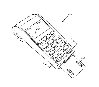
[0020] Figure 8 is a bank card chip reader device.
[0021] Figure 9 is an end view of the bank card chip reader device.
[0022] Figure 10 is a flowchart of a method of making a secure device.
[0023] Figure 11 is a magnetic field profile along a defined path.
[0024] Figure 12a, 12b, and 12c are three-dimensional representations
of the magnetic
flux density measured across the area resolved into three coordinate
components, Bõ, By, and B.
DETAILED DESCRIPTION
[0025] In the following description, reference is made to the
accompanying drawings
where like numerals represent like elements. The embodiments are described in
sufficient detail
to enable those skilled in the art to practice the present disclosure. It is
to be understood that
other embodiments may be utilized and that process, electrical, and mechanical
changes, etc.,
may be made without departing from the scope of the present disclosure.
Examples merely
3
CA 3038545 2019-03-29
typify possible variations. Portions and features of some embodiments may be
included in or
substituted for those of others. The following description, therefore, is not
to be taken in a
limiting sense and the scope of the present disclosure is defined only by the
appended claims and
their equivalents.
[0026] Referring now to the drawings and particularly to Figure 1, when an
ICC 1001 is
manufactured, it is typically packaged by being attached to a metal lead frame
1008 that is
connected to solder pads 1002 and 1003 by a wire bonds 1004 and 1005, and then
enclosed in an
encapsulant 1006 which is then cured. The encapsulated chip is then molded
into a plastic
housing 1007.
[0027] Referring now to Figure 2, in one embodiment of the invention, the
molded
plastic housing 1007 is replaced with the molded plastic housing or substrate
2007 where
dispersed in the substrate is a plurality of magnetized particles 4014. The
particles are
distributed randomly such that it is extremely difficult to reproduce the
exact distribution and
alignment of particles. Preferably, the particles are magnetized before
dispersion in the substrate
to add further randomness to the resulting magnetic field profile. Thus, the
substrate 2007 and
the particles 4014 form a physical unclonable function out of the molded
plastic housing.
[0028] The magnetic field profile near the surface of the ICC may be
measured by
an external magneto-resistive sensor (not shown), a Hall-effect sensor (not
shown), or an array of
such sensors, in close proximity to the top surface of the ICC. Since the
sensing elements are
typically around 0.3 ¨ 0.5 mm below the surface of the sensing device, the
average particle size
diameter using Hall-effect sensor or magneto-resistive sensor is preferably
greater than 0.1 mm.
Note that the diameter of a non-spherical particle is the diameter of the
smallest sphere that
encloses the particle. Other sensor options include magneto-optical sensor
technology, which is
capable of working with smaller magnetic particle sizes, but is more costly to
implement and
subject to contamination problems.
[0029] The magnetic field profile measurements may be taken within a
defined area or
along a defined path: straight, circular, or any arbitrarily selected and
defined path, and recorded
at the ICC foundry. Figure 11 shows a magnetic field profile along a defined
path where the
magnetic flux density has been resolved into three coordinate components Bx,
By, and B. Figure
12 shows a magnetic field profile measured over a rectangular area as would be
exhibited by the
defined area overlaying an ICC. The profile is a three-dimensional
representation of the
magnetic flux density measured across the area. The magnetic flux density
vector has been
resolved into three coordinate components, Bx, By, and Bz, shown separately in
Figures 12a, 12b,
4
CA 3038545 2019-03-29
and 12c. The magnetic field profile data would be signed by a private key and
written to the
1CC's non-volatile memory ("NVM") during programming. After installation of
the ICC onto a
circuit card, the magnetic "fingerprint" is once again read by an external
magneto-resistive
sensor and the magnetic profile is compared to the values stored on the chip
to authenticate the
ICC. This system would make it very difficult for counterfeit ICCs to make
their way into high
value applications. The system would be fairly inexpensive to implement with
almost
instantaneous authentication of the PUF over-molded ICCs.
[0030] Referring now to Figure 3, in a second embodiment of the
invention, the use of
magnetized particles 4014 creates a unique magnetic fingerprint that can be
applied to the
manufacture of ICCs by over-molding the encapsulated chip 1001 with a
substrate containing
magnetized particles 2007. The term "over-molded" is used here broadly to mean
anything from
adding a partial surface layer over the ICC to completely encasing the ICC.
One or more
sensors, such as a Hall-effect sensor 3001 is formed above the chip body and
encased within the
housing 2007. In this embodiment, the sensor(s) 3001 can record a series of
analog magnetic
intensity readings, in various locations along the substrate, in one, two, or
three coordinate
directions. Such an "internal" Hall-effect sensor can measure average particle
size diameters
that are less than 0.1 mm. Since these measurements are analog voltages, with
a sufficient
number of measurements and sufficient analog to digital resolution, unique
values can be derived
from the measurements. These values can be used for private keys, seeds, etc.
which are not
stored in the device's memory. Instead, they are read and derived by the
device "in flight" (i.e.,
during operation), thus rendering ineffective any probing attacks by
counterfeiters on the chip
itself. If a counterfeiter were to attempt to extract the private key from the
ICC, it is highly
probable that the over-molded magnetic layer will be disturbed and the private
key would be
lost.
[0031] These embodiments may, for example, be implemented on an integrated
circuit
chip on a printer or printer supply component, such as a toner cartridge, that
is used to
authenticate the toner cartridge for whatever purpose, as well as to perform
other functions such
as toner level monitoring, sheet count, etc.
[0032] A third embodiment of the invention is the application of the
PUF authentication
technology to bank cards and identification cards with an EMV transaction
chip. Bank cards
6001, for example, are under constant attack by counterfeiters. For this
reason an EMV
transaction chip 6002 mounted on a substrate 6003 that replaced the easily
counterfeited
magnetic strip 7001 shown in Figure 7, the back of the bank card 6001. To
avoid fraud, the
5
CA 3038545 2019-03-29
EMV transaction chip may be used with a personal identification number
("PIN"), but many
cards lack this extra protection for convenience of the customer, to reduce
data requirements in
transactions, and to avoid software upgrades for the PIN operation.
[0033] Bank cards with EMV transaction chips are mostly used in a
contact-based form:
the card is inserted into a reader, which creates a circuit that allows
handshaking between the
card and the payment terminal. A unique transaction is created that involves
cryptographic data
embedded in the chip.
[0034] For cards that require PINs, the transaction can't be completed
without the code,
which is not transmitted remotely as with debit and ATM transactions. Some
cards are equipped
with near-field communications (NFC) radios for contactless EMV transaction,
and will work
with point-of-sale systems.
[0035] A unique magnetic PUF signature of the analog magnetic intensity
readings could
replace the PIN requirement to authenticate the bank card. The PUF signature
would be a
second factor authentication for the bank card.
[0036] The substrate of a bank card may be fabricated where dispersed in
the substrate is
a plurality of magnetic particles. The particles are distributed randomly such
that it is extremely
difficult to reproduce the exact distribution and alignment of particles.
Thus, the substrate and
the particles of the bank card form a physical unclonable function. The
magnetic field profile
may be measured by an external sensor, such as a Hall-effect sensor (not
shown) in close
proximity to the bank card surface. Other sensor options include magneto-
optical sensor
technology. The magnetic field profile measurements may be taken within a
defined area or
along a defined path: straight, circular, or any arbitrarily selected and
defined path, and recorded
during manufacture of the bank card. The magnetic field profile data would be
written to the
EVM transaction chip's non-volatile memory.
[0037] When inserted into a card reader 8001, the reader could sweep a
sensor arm
across a portion of the bank card and one or more sensors, such as Hall-effect
sensors, located on
the sensor arm would measure the magnetic field in a defined area or along the
defined path. A
simple mechanical configuration with a drive cam would determine the path of
the sensor arm
sweep. Alternatively, as shown in Figure 9, the sensor or sensor array could
be at a fixed
location where the bank card slides across the sensors 8003, 8004, 8005, and
8006 as the bank
card is inserted into the reader slot 8002. Data corresponding to the magnetic
intensity readings
along the sensing path stored in the EMV transaction chip's non-volatile
memory and used to
6
CA 3038545 2019-03-29
validate the magnetic "fingerprint" detected by the card reader at time of the
transaction. This
invention does not require the user to remember a PIN, and the card reader can
perform the
validation locally. Alternatively, the card reader could be configured to
transmit the magnetic
"fingerprint" to the bank card company server or cloud location for remote
authentication when
high value transactions are taking place. Data that is stored in a cloud
location is stored in an
accessible network such as the Internet on physical storage devices such as
computer servers and
storage networks.
[0038] As an added layer of security, the EMV transaction chip on the
card could contain
information that would guide the card reader to read the magnetic
"fingerprint" in a specific
location on the bank card. This location could be different for different
cards and would add yet
another layer of complexity to the task of counterfeiting a bank card. A
varying position of the
magnetic "fingerprint" could also be configured to act as a rotating
encryption key. This rotating
key could change on a daily, weekly, or monthly basis. The rotating key could
be as simple as
two keys in which data is read off the "fingerprint" in a forward or reverse
motion, which would
be the least disruptive to current card reader configurations. Known
algorithms could be utilized
to determine when the "fingerprint" rotates.
[0039] In another embodiment, the bank card substrate to which the EMV
transaction
chip is mounted could be the location of a magnetic "fingerprint" such that
removal or alteration
of the EMV transaction chip would distort the substrate and thus alter the
magnetic "fingerprint,"
rendering the authentication inoperable. In a further embodiment, the bank
card could be
implemented in such a way as to cause tearing to the fingerprint if the chip
is removed.
[0040] The card reader may initiate the bank card authentication by
sending a request to
the EMV transaction chip on the bank card for data. The bank card EMV
transaction chip may
challenge the card reader and wait for a proper response (authenticating the
reader) before the
bank card security chip transmits the magnetic "fingerprint" authentication
data to the reader.
This challenge and response protocol makes it more difficult for
counterfeiters to acquire data
from the bank card. In addition to using the magnetic "fingerprint" or
signature of the bank card,
capacitive sensing technology may be used to detect the presence of the
randomly distributed
magnetized particles in the bank card, which could provide yet another
authentication step for
validating the bank card.
[0041] If at least one face of the bank card is non-opaque, the
presence of the magnetized
particles could be detected optically by a digital camera chip or by an
optical sensor. Similar to
capacitive sensing, this could provide an additional authentication step for
the bank card.
7
CA 3038545 2019-03-29
[0042] This technology could also be used in the same manner described
above to
authenticate access badges for secure facilities, or for other applications
such as passports,
government identification cards, driver licenses, etc. The PUF technology
could stand alone as a
security device, or in combination with a integrated circuit chip on the
identification card or
other security device having non-volatile memory.
[0043] Figure 4 shows a region of a substrate 4010. Dispersed in the
substrate is a
plurality of magnetized particles 4014. The particles are distributed randomly
such that it is
extremely difficult to reproduce the exact distribution and alignment of
particles. Thus, the
substrate 4010 and the particles 4014 form a PUF.
[0044] Figure 5 shows a side view of the substrate 4010 containing the
magnetized
particles 4014.
[0045] The field data may be measured while moving the PUF relative to
a stationary
magnetic field sensor(s) 5001, 5002, 5003 or by moving the magnetic field
sensor(s) 5001, 5002,
5003 next to a stationary PUF, etc. The sensors are shown in varying
orientations, but such a
varied orientation is not necessary. Multiple sensors may be used to reduce
the movement and
time required to measure the magnetic field over a desired area.
[0046] Figure 10 shows an example of a method of making a secure
device, such as an
integrated circuit chip with a PUF overlay or a bank card with an EMV
transaction chip with a
PUF substrate.
[0047] The magnetizable particles may be of any shape, and may contain
neodymium
and iron and boron. Alternatively, the magnetizable particles may contain
samarium and cobalt.
Preferably, the magnetized particles generate a sufficiently strong magnetic
field to be detected
with a low-cost detector.
[0048] Suitable substrate materials are used that allow formed
aggregate pellets of the
substrate material and particles to be magnetized. The magnetizable particles
are magnetized by,
for example, subjecting the pellets to a strong magnetic field. After
magnetization, the magnetic
particles do not clump together because the pellet carrier material is a
solid. During the molding
process, the pellets are heated and melted prior to molding.
[0049] The substrate carrier is then solidified in an ICC, overlaying
an ICC, encasing an
ICC, in the body of a bank card, or in the section of a bank card beneath the
section of a bank
card beneath the position of an EVM transaction chip. In an alternate
embodiment the carrier
8
CA 3038545 2019-03-29
may be, for example, a liquid that is caused to become solid by adding a
chemical, subjecting to
ultraviolet light, increasing its temperature, etc. Causing the carrier to
become solid locks the
distribution and orientation of the particles. In this case a high viscosity
liquid is preferred so
that the particles may be magnetized shortly before the material is molded.
The high viscosity
retards the movement of the magnetic particles toward each other while the
material is in a liquid
state and minimizes clumping of the magnetized particles. Clumping could cause
failures of the
over-molding process.
[0050] Magnetizing the particles in pellet form yields a more random
magnetic field
pattern, and is therefore more difficult to clone. Further, the application of
a magnetizing field
with patterned or randomized orientation may be applied to a formed substrate
with random
particle positions in order to cause greater diversity of magnetic field
orientation.
[0051] The foregoing description illustrates various aspects and
examples of the present
disclosure. It is not intended to be exhaustive. Rather, it is chosen to
illustrate the principles of
the present disclosure and its practical application to enable one of ordinary
skill in the art to
utilize the present disclosure, including its various modifications that
naturally follow. All
modifications and variations are contemplated within the scope of the present
disclosure as
determined by the appended claims. Relatively apparent modifications include
combining one or
more features of various embodiments with features of other embodiments.
9
CA 3038545 2019-03-29