Note : Les descriptions sont présentées dans la langue officielle dans laquelle elles ont été soumises.
85310947
DISTRIBUTED CONTROL SYNCHRONIZED RING NETWORK ARCHITECTURE
Related Applications
[0001] This application claims priority to U.S. Patent
Application 15/816,235 entitled "Distributed Control
Synchronized Ring Network Architecture", which was filed on
November 17, 2017, and which claims priority to U.S.
Provisional Patent Application 62/425,792, entitled
"Distributed Control Synchronized Ring Network Architecture",
which was filed on November 23, 2016.
Field of the Invention
[0002] The present invention relates to an improved ring
network architecture for achieving high bandwidth and low
latency on-chip communications.
Related Art
[0003] A conventional semiconductor chip may include an
extensive low-skew clock tree that distributes a global clock
signal to each of a plurality of circuit blocks fabricated on
the chip. The clock tree is designed to ensure that each of
the plurality of circuit blocks receives the same input clock
signal as each of the other circuit blocks. Implementing such
a global clock tree requires extensive layout (die) area and a
relatively complex interconnect structure (to enable point-to-
point communication, broadcast communication, arbitration and
synchronization). Pipeline stages are included along the
interconnect structure to maintain a minimum delay. In
addition, a centralized controller is required to establish
1
Date Recue/Date Received 2022-09-09
CA 03044672 2019-05-22
WO 2018/098084 PCT/US2017/062627
and control the global clock tree. As a result of these
structures, the global clock tree consumes a significant
amount of power.
[0004] Despite the above-described controls, clock skew may
eventually degrade the performance of the global clock tree.
The variance of the physical distance among all the
communication agents makes eliminating this clock skew
difficult.
[0005] It would therefore be desirable to have an improved
method and structure for implementing clock synchronization on
a semiconductor chip. It would be desirable for this improved
method and structure to be capable of providing high
frequency, low latency operation on a semiconductor chip,
without requiring a centralized controller. It would further
be desirable for this improved method and structure to have a
simply physical implementation, which does not require the use
of a low-skew, high power consumption clock tree over a large
area of the semiconductor chip.
SUMMARY
[0006] Accordingly, the present invention provides a ring
network architecture, wherein multiple communication nodes are
configured in a ring. The ring network architecture uses wave
pipelining to provide for high bandwidth and low latency on-
chip communications. A very high operating frequency can be
achieved using the ring network architecture of the present
invention. For example, assume each of the communication
nodes includes node logic for forwarding messages on the ring
network, wherein the node logic includes less than 12 levels
of logic with a fan-out of four (F04), with each logic gate
having a 100 picosecond (ps) gate delay. In this case, the
2
CA 03044672 2019-05-22
WO 2018/098084 PCT/US2017/062627
ring network architecture of the present invention is capable
of providing data transfer frequencies of 5 GHz or more, even
considering wire delays between nodes.
[0007] In accordance with one embodiment, each of the nodes
of the ring network implements a source-synchronized clocking
scheme, such that there is no need to build an extensive low
skew clock-tree across a large die area. The required control
logic is distributed among the nodes, such that no centralized
controller is necessary. The clocking and control schemes
implemented by the ring network architecture of the present
invention significantly simplify the physical implementation
of the network, while allowing for very high speed operation.
[0008] In accordance with one embodiment, a reference clock
signal is generated within a root node of the ring network.
This reference clock signal is routed through each of the
nodes of the ring network in a uni-directional manner.
Messages are transmitted between the nodes with the reference
clock signal, wherein each message received by a node is
clocked into the node using the corresponding received
reference clock signal. Each node of the ring network
includes a timestamp counter and a color bit register. The
timestamp counter of each node is updated using the received
reference clock signal each time a node generates and
transmits an original ordered message, and each time a node
receives an ordered message that it did not originally
generate. A pulse message continuously cycles through the
nodes of the ring network, wherein the pulse message toggles
the color bit register of a node each time the pulse message
is received by the node. Each of the timestamp counters and
color bit registers is initialized prior to normal operation,
such that each timestamp counter stores an identical timestamp
3
85310947
value and each color bit register stores an identical color bit
value. The timestamp values and color bit values enable each
node to resolve the transaction messages issued by the other
nodes in a precise order, even though the nodes are operating
independently, and receive the various transaction messages in
totally different timing orders. This capability provides a
powerful instrument for arbitration and synchronization.
[0009] In one embodiment, each node appends a timestamp value
from its timestamp counter to each ordered message generated.
Each node further includes a message snooper that stores the
ordered messages received on the ring network. When the color
bit is toggled within a node, the node analyzes the ordered
messages stored in its message snooper, and awards priority to
the ordered message having the oldest timestamp value.
[0010] The ring network architecture of the present invention
can be used, for example, to implement a MOSEI (Modified Owned
Shared Exclusive Invalid) cache coherence protocol memory bus or
a communication network on a massive parallel processor.
[0010a] According to one aspect of the present invention,
there is provided a distributed control synchronized ring
network on a semiconductor chip, comprising: a plurality of
nodes, including a root node and one or more branch nodes,
wherein the root node is coupled to receive a reference clock
signal; a circular clock signal path that routes the reference
clock signal from the root node, through each of the one or more
branch nodes, and back to the root node; and a circular message
path that extends in parallel with the circular clock signal
path, wherein the root node and the one or more branch nodes
transmit messages on the message path, wherein each of the
plurality of nodes includes corresponding node logic that
latches messages received on the message path in response to the
reference clock signal received on the clock signal path,
wherein each node of the plurality of nodes introduces a
corresponding node delay with respect to the reference clock
4
Date Recue/Date Received 2022-09-09
85310947
signal when transmitting messages, wherein the clock signal path
includes a delay line within each of the plurality of nodes,
wherein each delay line introduces a delay to the reference
clock signal on the clock signal path after the corresponding
node logic latches the messages received on the message path in
response to the reference clock signal, wherein the delay
introduced by the corresponding delay line within each of the
plurality of nodes is selected based on the corresponding node
delay.
[0011] The present invention will be more fully understood in
view of the following description and drawings.
BRIEF DESCRIPTION OF THE DRAWINGS
[0012] Fig. 1 is a block diagram of a distributed control
synchronized ring network in accordance with one embodiment of
the present invention.
[0013] Fig. 2 is a block diagram of a root node of the
distributed control synchronized ring network of Fig. 1 in
accordance with one embodiment of the present invention.
4a
Date Recue/Date Received 2022-09-09
CA 03044672 2019-05-22
WO 2018/098084 PCT/US2017/062627
[0014] Fig. 3 is a block diagram of a branch node of the
distributed control synchronized ring network of Fig. 1 in
accordance with one embodiment of the present invention.
[0015] Fig. 4 is a block diagram illustrating portions of
the root node of Fig. 2 and the branch node of Fig. 3 as used
for the source synchronous transmission of messages with a
clock signal in accordance with one embodiment of the present
invention.
[0016] Fig. 5 is a waveform diagram illustrating the source
synchronous timing of various signals of Fig. 4, in accordance
with one embodiment of the present invention.
[0017] Fig. 6 is flow diagram illustrating a method of
initializing the ring network of Fig. 1 in accordance with one
embodiment of the present invention.
[0018] Fig. 7 is flow diagram illustrating a method of
implementing a node initialization process the method of Fig.
6 in accordance with one embodiment of the present invention.
[0019] Figs. 8A, 8B, 8C, 8D, 8E, 8F, 8G, 8H and 81 are
tables that illustrate the status of the ring network during
the transmission of a point-to-point ordered message in
accordance with one embodiment of the present invention.
DETAILED DESCRIPTION
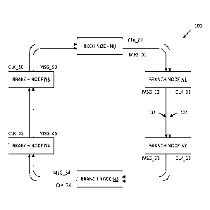
[0020] Fig. 1 is a block diagram of a distributed control
synchronized ring network 100 in accordance with one
embodiment of the present invention. Ring network 100
includes root node NO and branch nodes N1-N5, which are
connected in a ring. Although six communication nodes NO-N5
are included in the described examples, it is understood that
other numbers of nodes can be included in other embodiments.
However, each ring network will include one root node and one
CA 03044672 2019-05-22
WO 2018/098084 PCT/US2017/062627
or more branch nodes. Each of the nodes NO-N5 receives a
corresponding clock input signal and corresponding message
input signals, and transmits a corresponding clock output
signal and corresponding message output signals. The signals
of the ring network 100 are unidirectional. In the
illustrated embodiments, the signals of ring network 100 are
routed in a clockwise manner (although this is not necessary).
Each of the nodes NO-N5 has a transmitting neighbor and a
receiving neighbor. For example, branch node N3 includes
transmitting neighbor N2, and receiving neighbor N4. Nodes
NO, Ni, N2, N3, N4 and N5 transmit clock signals CLK_01,
CLK 12, CLK 23, CLK 34, CLK 45 and CLK 50, respectively, and
_ _ _ _ _
corresponding output messages MSG 01, MSG 12, MSG_23, MSG 34,
MSG _ 45, and MSG 50, respectively, to receiving neighbors N1,
_
N2, N3, N4, N5 and NO, respectively. The clock signals
CLK 01, CLK 12, CLK 23, CLK 34, CLK 45 and CLK 50 are
_ _ _ _ _ _
transmitted on a clock path 101 of the ring network 100, and
the messages MSG 01, MSG 12, MSG 23, MSG 34, MSG 45, and
MSG 50 are transmitted on a message bus 102 of the ring
_
network 100.
[0021] Fig. 2 is a block diagram illustrating root node NO
in more detail in accordance with one embodiment of the
present invention. Root node NO includes master clock
generator 201, delay line 202, resynchronizer 205, node logic
210, synchronizer 220, message snooper 230, receive first in
first out (FIFO) memory 231, transmit FIFO memory 232, client
logic 240, node identifier (ID) memory 250, color bit register
251, time stamp (TS) counter 255, message assembler 260 and
multiplexer 265.
[0022] In general, root node NO includes circuitry that
operates in two clock domains, including a ring network clock
6
CA 03044672 2019-05-22
WO 2018/098084 PCT/US2017/062627
domain (specified by reference clock CK REF) and a client
logic clock domain (specified by local clock signal CKO). The
division between these clock domains is illustrated by dashed
line 270 in Fig. 2. Thus, client logic 240 and transfers
between client logic 240 and color bit register 251, node ID
register 250, timestamp counter 255, message snooper 230,
receive FIFO 231 and transmit FIFO 232 are performed in the
client logic clock domain. Clock generator 201, delay line
202, resynchronizer 205, node logic 210, node identifier (ID)
memory 250, color bit register 251, time stamp (TS) counter
255, message assembler 260 and multiplexer 265 operate in the
ring network clock domain. In addition, write operations to
message snooper 230 and receive FIFO 231 and read operations
from transmit FIFO 232 are performed in the ring network clock
domain. In accordance with one embodiment, synchronization
circuit 220 (which receives the reference clock signal OK REF
and the local clock signal CKO) performs the synchronization
between the ring network clock domain and the client logic
clock domain using resynchronization methods known in the art.
The requirements of the ring network clock domain and the
client logic clock domain are described in more detail below.
[0023] Master clock generator 201 of root node NO generates
the reference clock signal CK_REF of the ring network 100.
Conventional clock generation circuitry (e.g., a phase locked
loop circuit) can be used to generate the reference clock
signal CK_REF. In the described embodiments, the reference
clock signal OK REF has a frequency of about 5 GHz or more.
However, it is understood that the reference clock signal
CK_REF can have other frequencies in other embodiments. The
frequency and voltage of the reference clock signal OK _REF can
be scaled based on the bandwidth demands and power
7
CA 03044672 2019-05-22
WO 2018/098084 PCT/US2017/062627
optimization of the ring network architecture. Note that a
setup process (described below) can be performed at a lower
reference clock frequency than normal operation, so that the
wire delay between nodes NO-N5 has no impact on the setup
process. Note that root node NO is the only node that
includes a master clock generator 201. As described in more
detail below, each of the branch nodes Ni, N2, N3, N4 and N5
operate in response to the corresponding clock signals CLK_01,
CLK 12, CLK 23, CLK 34 and CLK 45 sent by their transmitting
_ _ _ _
neighbors NO, Ni, N2, N3 and N4. That is, the reference clock
signal CK_REF is effectively transmitted through branch nodes
NO-N5 in series.
[0024] Root node NO uses the reference clock signal OK REF
to synchronize the incoming message MSG_50 (sent by
transmitting neighbor N5 along with incoming clock signal
CLK 50). More specifically, the incoming message MSG 50 was
_ _
initially synchronized to the network clock domain of the
transmitting neighbor N5. As a result, clock domain crossing
synchronization is necessary within the root node NO (i.e.,
the message MSG50 received from the transmitting neighbor N5
must be resynchronized with the reference clock signal OK REF
within root node NO). In one embodiment, resynchronization
circuit 205 performs this resynchronizing operation by
latching the incoming message MSG 50 into a first flip-flop in
response to the incoming clock signal CLK_50. The message
MSG 50 provided at the output of the first flip-flop is then
_
latched into a second flip flop in response to the reference
clock signal CK_REF. The second flip-flop provides the
synchronized message MSG_O, which is provided to node logic
210. This synchronized message MSG_O is stored in node logic
210 in response to the reference clock signal CK_REF.
8
CA 03044672 2019-05-22
WO 2018/098084 PCT/US2017/062627
[ 0025 ] Fig. 3 is a block diagram illustrating branch node
Ni in more detail. In the described embodiments, branch nodes
N2-N5 are substantially identical to branch node Ni (although
these nodes may implement different client logic). Branch
node Ni includes clock delay line 302, node logic 310,
synchronization circuit 320, message snooper 330, receive FIFO
memory 331, transmit FIFO memory 332, client logic 340, node
identifier (ID) memory 350, color bit register 351, time stamp
(TS) counter 355, message assembler 360 and multiplexer 365.
Note that the above-listed elements of branch node Ni are
similar to the similarly named elements of root node NO. The
client logic 340 of node Ni operates in response to a local
node clock domain signal CK1. Dashed line 370 designates the
boundary of the local clock domain (CK1) and the ring network
clock domain (CK REF), wherein synchronization circuit 320
_
provides for communications across these clock domains. Note
that branch node Ni does not include circuits equivalent to
the master clock generator 201 or the resynchronizer 205 of
root node NO. That is, root node NO includes the only master
clock generator 201 of ring network 100.
[0026] The timing of the source synchronous transmission of
messages and clock signals from root node NO to branch node Ni
will now be described. Note that transmission between other
nodes is performed in the same manner as transmission from
node NO to node Ni.
[0027] Fig. 4 is a block diagram illustrating relevant
portions of nodes NO and Ni for the transmission of messages
and clock signals from node NO to Ni, including node logic
210, delay line 202, message assembler 260, multiplexer 265,
ring network clock signal path 101, ring network message bus
102 and node logic 310. Fig. 5 is a waveform diagram
9
CA 03044672 2019-05-22
WO 2018/098084
PCT/US2017/062627
illustrating the source synchronous timing of various signals
of Fig. 4, in accordance with one embodiment of the present
invention.
[0028] In general, node NO can transmit output messages on
two paths. In the first path, the message MSG_O received by
node logic 210 is forwarded to node logic Ni. In this case,
node logic 210 determines that the received message MSG 0
should be forwarded (e.g., determines that the received
message MSG_O does not address node NO), and forwards the
message to multiplexer 265. Multiplexer 265 is controlled to
route this message as the output message MSG_01 (which is
designated as MSG01IN in Figs. 4 and 5). Node logic 210 and
multiplexer 265 introduce a node delay DNO with respect to the
reference clock signal OK REF.
[0029] In the second path, a message MSG_OCL provided by
client logic 240 is routed through transmit FIFO 232 and
provided to message assembler 260 (in response to the
reference clock signal CK REF). Message assembler 260
provides required information (e.g., a timestamp value from
timestamp counter 250 and the node ID value from node ID
memory 350) to the message MSG OcLf and provides the resulting
message to multiplexer 265. Multiplexer 265 is controlled to
route this message as the output message MSG_01 (which is
designated as MSG 01IN in Figs. 4 and 5). Message assembler
260 and multiplexer 265 introduce the node delay DNO to the
message MSGOcL, with respect to the reference clock signal
OK REF. In one embodiment, message assembler 260 and node
logic 210 are designed such that these circuits introduce the
same (or a similar) delay to the received messages MSG_OcL and
MSG_O, respectively, with respect to the reference clock
signal OK REF. Fig. 5 illustrates the node delay DNO that
CA 03044672 2019-05-22
WO 2018/098084 PCT/US2017/062627
exists between the reference clock signal and the transmitted
message MSG_OlIN for either the message MSG_O or the message
MSG_OcL.
[0030] Although the messages MSG 0 and MSG OCL are described
generically in the example of Figs. 4 and 5, the details of
these messages (and associated message 'types', including
broadcast messages, read-modify-write messages, point-to-point
unordered messages and point-to-point ordered messages) are
described in more detail below.
[0031] Because the transmitted message MSG 011N is delayed
with respect to the reference clock signal CK_REF, delay line
202 is used to add a delay D202 to the reference clock signal
CK REF, thereby creating the output clock signal CLK 01 of
root node NO (shown as clock signal CLK_OlIN in Figs. 4 and 5).
The delay D202 introduced by delay line 202 is selected to
ensure that the clock signal CLK_OlIN has a proper setup and
hold time with respect to the message MSG_OlIN transmitted from
node NO. In one embodiment, the delay D202 of delay line 202
is equalized to the node delay Dm) described above. That is,
the transmitted message MSG 011N is synchronized to the output
clock signal CLK 011N using the known internal delays of the
node NO. In accordance with one embodiment, the delay D202 is
adjustable (e.g., can be lengthened or shorted as desired
under the control of node logic 210 and/or client logic 240).
[0032] Note that the structures 101D and 102D used to
implement the clock signal path 101 and the message bus 102
between nodes NO and Ni may exhibit significant delays (e.g.,
buffer delays). The delays introduced by clock signal line
structure 101D and the message bus structure 102D are
designated as delays Dioi and D102, respectively. Thus, the
clock signal CLK_OlouT received by node Ni is delayed by D101
11
CA 03044672 2019-05-22
WO 2018/098084 PCT/US2017/062627
with respect to the clock signal CLK 011N transmitted by node
NO. Similarly, the message MSG_OlouT received by node Ni is
delayed by D102 with respect to the message MSG 11N transmitted
by node NO. This relationship is shown in Fig. 5. In order
to maintain the desired setup and hold times established by
node NO (when generating CLK_OlIN and MSG_OlIN), the delays Dioi
and D102 must be the same. It is therefore very important that
the wires and buffers used to implement the clock signal line
structure 101D and the message bus structure 102D are highly
equalized and balanced in order to minimize setup and hold
time loss. That is, the clock path structure 101D and message
bus structure 102D should provide substantially identical
transmission characteristics between nodes NO and Ni, such
that the relative phases of the transmitted clock signal
CLK_OlIN and the transmitted message MSG_OlIN are maintained at
the receiving node Ni by received clock signal CLK_Oloin, and
received message MSGmOlour.
[0033] In accordance with the above-described example, the
clock path 101 and the message bus 102 operate as a wave
pipeline system, wherein messages transmitted on the message
bus 102 are latched into the receiving node in a source-
synchronous manner using the clock signal transmitted on the
clock path 101. In this manner, messages are transmitted from
node NO to node Ni at the frequency of the reference clock
signal CK_REF, allowing for fast data transfer from node NO to
node Ni. During normal operation, the node logic within each
of the nodes NO-N5 latches incoming messages in response to
the received clock signal (e.g., node logic 210 and 310 latch
the incoming messages MSG_O and MSG_01, respectively, in
response to the received clock signals CK_REF and CLK_01,
respectively).
12
CA 03044672 2019-05-22
WO 2018/098084 PCT/US2017/062627
[0034] Because wave pipelining is implemented, the wire and
buffer delays Dioi and Dm of the clock signal line structure
1010 and the message bus structure 102D will not degrade the
operating frequency of the ring network 100. Note that the
wave pipelining may allow a transmitting node to send a first
message to a receiving node, and then send a second message to
the receiving node, before the receiving node has received the
first message. That is, there may be a plurality of messages
simultaneously propagating from node NO to node Ni on the
message bus structure 102D. Note that this may occur if the
period of the reference clock signal CK_REF (e.g., 200 ps for
a 5 GHz clock) is less than the wire/buffer delay Dlojin
-loz
between the adjacent nodes NO and Ni. In accordance with one
embodiment, the wire/buffer delay D101/D102 between each pair of
adjacent nodes must be long enough (i.e., exhibit a minimum
delay) to ensure that a first plurality of messages being
transmitted from a first node (e.g., node NO) to an adjacent
second node (e.g., node Ni) do not overtake a second plurality
of messages being transmitted from the second node (e.g., node
Ni) to an adjacent third node (e.g., node N2).
[0035] In one embodiment, the gate delay of the node logic
210 and multiplexer 265 may determine the maximum frequency of
the reference clock signal CK_REF. For maximum efficiency,
the period of the generated reference clock signal CK REF
should be equalized to the node delay DNO. In one embodiment,
the node logic 210 includes sequential logic (e.g., 10 levels
of fan out 4 (F04) logic), which allows the reference clock
signal CK_REF to have a frequency of 5 GHz or greater.
[0036] Because the node logic 210 has a relatively simple
design, communications between the nodes NO-N5 of the ring
network can be performed at a relatively high frequency.
13
CA 03044672 2019-05-22
WO 2018/098084 PCT/US2017/062627
Client logic 240 typically includes a more complicated design,
and may operate at a slower frequency than the frequency of
the reference clock signal CK_REF. That is, while client
logic 240 may receive messages from the ring network at the
frequency of the reference clock signal CK_REF, the client
logic 240 is not required to respond at the frequency of the
reference clock signal CK REF.
[0037] In an alternate embodiment, the ring network 100 can
also be operated in response to a reference clock signal
CK REF having a relatively low frequency, wherein the period
of the reference clock signal CK_REF is greater than the
wire/buffer delay D101/D102 between adjacent nodes. In this
case, each message transmitted by a node is received (and
latched) by the adjacent node before the transmitting node
sends the next message. In this embodiment, the wire/buffer
delay D101/D102 between adjacent nodes has no impact on the
signal pipeline. In one embodiment, the reference clock
signal CK REF is reduced to such a low frequency during a
setup phase (described below), but is increased to a high
frequency (e.g., 5GHz or more) during normal operation.
[0038] The set-up of the nodes NO-N5 of ring network 100
will now be described.
[0039] Fig. 6 is a flow diagram 600 illustrating a method
of initializing ring network 100 in accordance with one
embodiment of the present invention. As illustrated by step
601 of Fig. 6, a setup process is started (e.g., by activating
the RESET signal provided to client logic 240 of root node
NO). In response, client logic 240 starts a node
initialization process (Step 602), wherein the node ID values
stored in the node ID registers of nodes NO-N5 are
initialized, the color bits stored in the color bit registers
14
CA 03044672 2019-05-22
WO 2018/098084 PCT/US2017/062627
of nodes NO-N5 are reset to a predetermined value (e.g., '0'),
and the time stamp values stored by the time stamp counters
within each of the nodes NO-N5 are reset to a predetermined
value (e.g., '0'). As illustrated by step 603 of Fig. 6, a
pulse message, which cycles through each of the nodes NO-N5,
is initiated (e.g., by activating the PULSE signal provided to
client logic 240 of root node NO). Normal operation of the
ring network 100 then begins (Step 604).
[0040] Fig. 7 is a flow diagram 700 illustrating a method
of implementing the node initialization process of step 602 in
accordance with one embodiment of the present invention. Root
node NO is hardwired such that node ID register 250 stores a
node ID value equal to '0'. In response to receiving the
activated RESET signal, client logic 240 generates an ID setup
message, which is a read-modify-write message (step 701).
This ID setup message includes an node ID field, which is
_
initially set to have a value of '0' (based on the node ID
value stored by node ID register 250 of node NO). Client
logic 240 also resets its timestamp counter 255 to store a
timestamp value of '0', and also resets its color bit register
251 to store a color bit value of '0' (Step 702). Client
logic 240 transmits the ID setup message to adjacent receiving
node Ni (via transmit FIFO 232, message assembler 260 and
multiplexer 265). This ID setup message is synchronized with
the reference clock signal CK_REF in the manner described
above in connection with Figs. 4 and 5.
[0041] Node logic 310 receives the ID setup message (using
the corresponding clock signal CLK_01) within node Ni. Node
logic 310 sends the ID setup message to the client logic 340
within node Ni (via receive FIFO 331). In response, client
logic 340 increments the ID value in the ID field of the
CA 03044672 2019-05-22
WO 2018/098084 PCT/US2017/062627
ID setup message by one (Step 703). Client logic 340 then
writes the updated ID value (e.g., '1') to its node ID
register 350 (step 704). Client logic 340 also resets its
timestamp counter 355 to store a timestamp value of '0', and
also resets its color bit register 351 to store a color bit
value of 10' (Step 705). Thus, branch node Ni is assigned an
node ID value equal to '1', a timestamp value equal to '0' and
a color bit value equal to '0'.
[0042] The client logic 340 transmits the modified ID setup
message, which includes the updated node ID value, to the
adjacent receiving node N2 (via transmit FIFO 332, message
assembler 360 and multiplexer 365) (Step 706).
[0043] If the downstream receiving node is the root node NO
(step 707, YES branch), then the ID setup operation is
complete (step 708). If the downstream receiving node is not
the root node NO (step 707, NO branch), then processing
returns to step 703, whereby the client logic in the receiving
branch node increments the node ID value in the ID setup
message by one (step 703), stores the incremented node ID
value in its node ID register (step 704), and resets its
timestamp counter and color bit (step 705). This process
continues such that nodes NO to N5 are assigned unique node ID
values of 0 to 5, respectively. At the end of the ID_setup
operation, the timestamp counters of nodes NO-N5 all store the
same timestamp value (e.g., '0') and the same color bit value
(e.g., 10').
[0044] After the node initialization process is complete,
the client logic 240 in node NO transmits a pulse message on
ring network 100. In one embodiment, the pulse message is
initiated by an activated PULSE signal provided to client
logic 240). In an alternate embodiment, client logic 240
16
CA 03044672 2019-05-22
WO 2018/098084 PCT/US2017/062627
initiates the pulse message in response to receiving the
modified ID setup message from transmitting node NS. The
_
pulse message continuously traverses the ring network 100.
The pulse message is sequentially provided to the node logic
within nodes NO-N5. Each time that the node logic within a
node receives the pulse message, the node logic toggles the
color bit value stored in its corresponding color bit
register. For example, the first time that node logic 310 in
node Ni receives the pulse message from node NO, the node
logic 310 changes the value of the color bit stored in color
bit register 351 from '0' to '1'. As described in more detail
below, the color bits are used in the arbitration of ordered
messages received by the nodes NO-N5.
[0045] After completing the above-described setup process,
nodes NO-N5 are ready for normal operation. Normal operation
of ring network 100 in accordance with one embodiment of the
present invention will now be described.
[0046] The client logic (e.g., client logic 240) of nodes
NO-N5 communicate by exchanging messages through the message
bus 102. The width and the format of the message bus 102 must
satisfy the following requirements. Message bus 102 must be
able to encapsulate all of the message types described in more
detail below. Message bus 102 is also designed to provide the
required bandwidth and timing, while minimizing the required
layout area of the wires/buffers.
[0047] In one embodiment, four message types are
implemented on message bus 102, including: 1) broadcast
messages, 2) read-modify-write messages, 3) point-to-point
unordered messages and 4) point-to-point ordered messages.
Most of these messages are generated by the client logic
17
CA 03044672 2019-05-22
WO 2018/098084 PCT/US2017/062627
within the nodes NO-N5, which may include, for example, a
central processing unit (CPU) or a memory controller.
[0048] In a broadcast message, the client logic of the
transmitting node (e.g., client logic 240 of node NO) sends
the broadcast message to its receiving neighbor (e.g., node
Ni, via transmit FIFO 232, message assembler 260 and
multiplexer 265). The node logic within the receiving
neighbor (e.g., node logic 310) receives the broadcast
message. In response, this node logic routes the broadcast
message to its corresponding client logic (e.g., client logic
340, via its corresponding receive FIFO 331). This node logic
also forwards the broadcast message to its receiving neighbor
(e.g., node N2, via multiplexer 365.) The forwarding is
stopped when the original transmitting node (e.g., node NO)
receives the broadcast message from its transmitting neighbor
(e.g., node NS). For example, a cache line invalidation
request may be transmitted as a broadcast message.
[0049] In a read-modify-write message, the client logic of
the transmitting node (e.g., client logic 240 of node NO)
sends a message to its receiving neighbor (e.g., node Ni, via
transmit FIFO 232, message assembler 260 and multiplexer 265).
The node logic within the receiving neighbor (e.g., node logic
310) receives the read-modify-write message, and forwards this
message to its corresponding client logic (e.g., client logic
340, via its corresponding receive FIFO 331). This client
logic may modify the message, if necessary. The client logic
subsequently forwards the read-modify-write message to its
receiving neighbor (e.g., node N2, via transmit FIFO 332,
message assembler 360 and multiplexer 365). Note that the
client logic will forward the read-modify-write message at its
own discretion (e.g., using corresponding flow control and
18
CA 03044672 2019-05-22
WO 2018/098084 PCT/US2017/062627
bandwidth allocation logic), which may be some number of
cycles (of the local clock signal) after receiving the read-
modify-write message. This forwarding process is repeated by
each of the nodes, until the read-modify-write message is
returned to the original transmitting node (e.g., node NO) by
its transmitting neighbor (e.g., node N5). The original
transmitting node processes the received read-modify-write,
and stops the propagation of the read-modify-write message.
The ID setup message described above in connection with the
_
setup process is an example of a read-modify-write message.
In accordance with another example, a cache-line snoop
response from a CPU may be transmitted as a read-modify-write
message.
[0050] In a point-to-point unordered message, the client
logic of the transmitting node (e.g., client logic 240 of node
NO) sends a message to its receiving neighbor (e.g., node Ni,
via transmit FIFO 232, message assembler 260 and multiplexer
265). The point-to-point unordered message addresses a
particular one of the other nodes (e.g., node N2), wherein the
node ID value of the addressed node is included in the
message. The node logic within each intermediate node between
the transmitting node and the addressed node forwards the
message to its receiving neighbor, until the message reaches
the addressed node. For example, the node logic 310 in node
Ni may receive a point-to-point unordered message from node
NO, compare its node ID value (e.g., '1') with the node ID
value included in the message (e.g., '2'), and in response,
determine that the message does not address node Ni. In
response, node logic 310 forwards the point-to-point unordered
message to receiving node N2 (via multiplexer 365). Note that
the node logic 310 does not forward the message to the client
19
CA 03044672 2019-05-22
WO 2018/098084 PCT/US2017/062627
logic 340 within the non-addressed node Ni. Upon receiving
the point-to-point unordered message, the node logic within
node N2 would then determine that the node ID value included
in the point-to-point unordered message (e.g., '2') is equal
to its own node ID value (e.g., '2'), and in response, provide
the point-to-point unordered message to its corresponding
client logic (via its corresponding receive FIFO). The point-
to-point unordered message is not transmitted beyond the
addressed node on the ring network 100 (e.g., node N2 does not
forward the point-to-point unordered message to node N3). In
one embodiment, a data response to a read request may be
transmitted as a point-to-point unordered message.
[0051] In a point-to-point ordered message, the client
logic of the transmitting node (e.g., client logic 240 of node
NO) sends a message to its receiving neighbor (e.g., node Ni,
via transmit FIFO 232, message assembler 260 and multiplexer
265). The point-to-point ordered message addresses a
particular one of the other nodes (e.g., node N2), wherein the
node ID value of the addressed node is included in the
message. The transmitting node also attaches its own unique
node ID value from its own node ID register (e.g., node ID
value '0' from node ID register 250) and a current time stamp
value (TS) from its own time stamp counter (e.g., time stamp
counter 255) to the message. Within the transmitting node
(e.g. node NO), the message assembler 260 increments the time
stamp counter 255 upon transmitting the point-to-point ordered
message.
[0052] The node logic within each intermediate node (e.g.,
node Ni) between the transmitting node and the addressed node
compares its node ID value (e.g., '1') with the addressed node
ID value included in the point-to-point ordered message (e.g.,
CA 03044672 2019-05-22
WO 2018/098084 PCT/US2017/062627
'2'), and in response, determines that the message does not
address this intermediate node. In response, the node logic
310 of this intermediate node Ni forwards the point-to-point
ordered message to its corresponding receiving node N2 (via
multiplexer 365). Upon receiving the point-to-point ordered
message, the node logic in each node increments its
corresponding timestamp counter, and stores the ordered
message in its message snooper (e.g., within node N1, node
logic 310 increments its timestamp counter 355 and stores the
ordered message in its message snooper 330).
[0053] Upon receiving the point-to-point ordered message,
the node logic within the addressed node (e.g., node N2)
increments its timestamp counter, and determines that the
addressed node ID value included in the point-to-point ordered
message is equal to its own node ID value (e.g., '2'). In
response, the node logic within the addressed node N2 causes
the color bit value stored in its color bit register to be
stored in its message snooper, along with the point-to-point
ordered message. The node logic within the addressed node N2
then forwards the ordered message to its corresponding
receiving node (e.g., node N3). This forwarding continues
until the ordered message reaches the original transmitting
node (e.g., node NO), wherein each intermediate node
increments its timestamp counter and captures the ordered
message into its message snooper. Upon receiving the ordered
message, the original transmitting node (e.g., node NO) does
not increment its timestamp counter. At this time, the
original transmitting node can determine whether its ordered
message will be awarded priority by the addressed node by
examining the contents of its own message snooper. The
addressed node waits until the pulse message changes the state
21
CA 03044672 2019-05-22
WO 2018/098084 PCT/US2017/062627
of the color bit stored in its corresponding color bit
register to resolve the priority of the point-to-point ordered
message. In this manner, the information in the message
snooper in each node provides a consistent view of the order
in which messages are issued, even though messages are
received by each node in different orders. The information in
the message snoopers will be used for arbitration and conflict
resolution in a manner described in more detail below.
[0054] As described above, each of the nodes NO-N5
temporarily stores each of the received point-to-point ordered
messages into its message snooper (e.g., message snoopers 230
and 330 of nodes NO and Ni store the ordered messages received
by node logic 210 and 310, respectively). In the described
embodiments, each of the message snoopers is a FIFO, wherein
the depth of the message snooper FIFO is a design parameter of
the ring network 100. In one embodiment, the depth of each
message snooper is selected to provide an appropriate tradeoff
in layout area, operating speed, power consumption and
required bandwidth. As described below, the depth of the
message snooper limits the number of point-to-point ordered
message requests that can be outstanding on the ring network
100 at any given time.
[0055] In accordance with one embodiment, each node of the
ring network 100 is assigned a quota of point-to-point ordered
message requests, wherein this quota ranges from 0 to a value
equal to the depth of the message snooper minus one. Each
node cannot have a number of outstanding point-to-point
ordered messages exceeding its quota, wherein a point-to-point
ordered message is considered outstanding until it has looped
back to its originating node. The quota assigned to each node
does not need to be the same. For example, the quota of a
22
CA 03044672 2019-05-22
WO 2018/098084 PCT/US2017/062627
node not capable of sending out point-to-point ordered
messages can be set to zero, while a performance critical node
(e.g., a CPU) can be assigned a larger quota of point-to-point
ordered messages. However, the total number of possible
outstanding point-to-point ordered message requests (e.g., the
sum of the quotas assigned to each of the nodes NO-N5) must be
less than the depth of the message snooper.
[0056] Each message snooper captures the point-to-point
ordered messages passing through the corresponding node. As
described in more detail below, these captured ordered
messages are used to identify the order in which the messages
were issued on the ring network 100.
[0057] As described above, each of the timestamp counters
in nodes NO-N5 is initialized to a value of '0', and each is
incremented when the corresponding node transmits an original
point-to-point ordered message, or receives a point-to-point
ordered message that originated in another node. Each of the
timestamp counters counts up to a MAX COUNT value. After
reaching the MAX _COUNT value, the timestamp counters wrap
around to a value of '0'. In one embodiment, the MAX COUNT
value is selected to be at least two times the number of
entries of each message snooper to avoid counter aliasing.
[0058] In one embodiment, initializing (or wrapping around)
the timestamp counter also inverts a sign bit of the timestamp
counter value. As described in more detail below, the nodes
NO-N5 use the timestamp value (and the sign bit) to determine
the order of point-to-point ordered messages received on the
message bus 102.
[0059] In general, if the sign bits of the timestamp values
associated with two point-to-point ordered messages are equal,
then the point-to-point ordered message with a lower timestamp
23
CA 03044672 2019-05-22
WO 2018/098084
PCT/US2017/062627
value is older (and therefore has priority). If the sign bits
of the timestamp values associated with two point-to-point
ordered messages are different, then the point-to-point
ordered message with a higher timestamp value is older (and
therefore has priority). If the sign bits and timestamp
values associated with two point-to-point ordered messages are
equal, then the two point-to-point ordered messages were sent
at the same time. Under these conditions, a 'tie-breaker' is
necessary to provide a resolution. For example, an address
hashing function may be applied to each point-to-point ordered
message to generate a random value. The point-to-point
ordered message associated with the larger value may be
designated as the older message and awarded priority. Other
methods can also be used to provide a priority resolution
under these conditions.
[0060] The
manner in which the priority of point-to-point
ordered messages is determined in accordance with one
embodiment of the present invention will now be described in
more detail, using a specific example. In this example, the
client logic 240 of root node NO includes a first CPU (e.g.,
CPU 0), the client logic of branch node N3 includes a second
CPU (e.g., CPU_1), and the client logic of branch node N5
includes a system memory. Both CPU_O (node NO) and CPU_1
(node N3) attempt an exclusive access to the same cache line
'A' in the system memory of node N5. In the described
example, it is assumed that the timestamp counter of each of
the nodes NO-N5 initially has a value of '0'.
[0061] Fig.
8A is a table 800 that illustrates the status
of the ring network 100 at time TO, including: the actions
performed by nodes NO-N5, the output messages provided on the
message bus 102 by nodes NO-N5, and the contents of the
24
CA 03044672 2019-05-22
WO 2018/098084 PCT/US2017/062627
message snoopers of nodes NO-N5, the values of the timestamp
counters of nodes NO-N5, the values of the color bits of nodes
NO-N5, and the location of the pulse message that continuously
travels around the ring network 100. At time TO, the CPU 0 of
root node NO transmits a message M*0_5(0) on the message bus
102 (e.g., as MSG_01). In the examples described herein, a
message bus notation of M*X Y(Z) is used, wherein M* specifies
a point-to-point ordered message, X specifies the source node
ID (i.e., the contents of the node ID register 250 of the node
NO that originates the message), Y corresponds with the
destination node ID (i.e., the contents of the node ID
register of the node N5 to receive the point-to-point ordered
message), and Z corresponds with the timestamp value of the
originating node NO (at the time the message is initially
sent). Thus, message M*0_5(0) specifies a point-to-point
ordered message transmitted from node NO to node N5, initiated
when the timestamp counter of node NO has a value of O. In
the described example, message M*0 5(0) includes additional
information (not shown) that indicates that the transaction is
an access to a cache line 'A' in the system memory of node N5.
Upon transmitting the point-to-point ordered message M*0 5(0)
on the message bus 102, the CPU_O of node NO increments its
timestamp counter 255 from a value of 0 to a value of 1. The
message snooper 230 of node NO stores the message M*0 5(0).
[0062] Also at time TO, the node N2 transmits an ordered
point-to-point message M*2_4(0) on the message bus 102 (e.g.,
as MSG 23). In accordance with the nomenclature defined
above, message M*2_4(0) specifies a point-to-point ordered
message transmitted from node N2 to node N4, initiated when
the timestamp counter of node N2 has a value of O. Upon
transmitting the point-to-point ordered message M*2_4(0) on
CA 03044672 2019-05-22
WO 2018/098084 PCT/US2017/062627
the message bus 102, the node N2 increments its timestamp
counter from a value of 0 to a value of 1. The message
snooper of node N2 stores the message M*2_4(0).
[0063] Note that at time TO, nodes Ni and N3-N5 do not
initiate any actions (or provide any messages on the message
bus 102) and the message snoopers of nodes Ni and N3-N5 are
empty. Because none of these nodes Ni and N3-N5 has received
or transmitted a point-to-point ordered message, the timestamp
counters of these nodes remain unchanged.
[0064] In the illustrated example, the pulse message
reaches node N4 at time TO, thereby causing the color bit of
node N4 to transition from a 10' value to a 11' value. Note
that the color bit values and the pulse location are
arbitrarily selected for the present example.
[0065] Fig. 8B is a table 801 that illustrates the status
of the ring network 100 during the next cycle Ti. At this
time, none of the nodes NO-N5 transmit any new messages. The
message M*0 5(0) is received by node Ni, and this node Ni
stores the message M*0_5(0) in its message snooper. Because
node Ni has received a point-to-point ordered message, node Ni
increments its timestamp counter from 0 to 1. The node logic
310 within node Ni then transmits the point-to-point ordered
message M*0_5(0) to node N2.
[0066] In addition, the point-to-point ordered message
M*2 4(0) is received by node N3, and this node N3 stores the
_
message M*2_4(0) in its message snooper. Because node N3 has
received a point-to-point ordered message, node N3 increments
its timestamp counter from 0 to 1. The node logic within node
N3 then transmits the point-to-point ordered message M*2_4(0)
to node N4.
26
CA 03044672 2019-05-22
WO 2018/098084 PCT/US2017/062627
[ 0067 ] The pulse message reaches node N5 during cycle Ti,
thereby causing the color bit of node N5 to toggle from a '0'
value to a '1' value.
[0068] Fig. 80 is a table 802 that illustrates the status
of the ring network 100 during the next cycle T2. During this
cycle T2, the CPU_1 of node N3 transmits a message M*3_5(1) on
the message bus 102 (e.g., as MSG 34) and stores this message
M*3_5(1) in its message snooper. As described above, message
M*3_5(1) specifies a point-to-point ordered message from node
N3 to node N5. Note that the timestamp value of node N3 is
'1' at the time the message M*3_5(1) is generated. In the
described example, message M*3_5(1) includes additional
information (not shown) that indicates that the transaction is
an access to a cache line IIV in the system memory of node N5.
Because node N3 has transmitted an ordered message M*3_5(1),
the timestamp counter of node N3 is incremented, from 1 to 2.
Note that nodes NO-N2 and N4-N5 do not initiate any new
actions during cycle T2.
[0069] Also during cycle T2, the point-to-point ordered
message M*0_5(0) is received by node N2, and this node N2
stores the message M*0 5(0) in its message snooper. Because
node N2 has received an ordered message, node N2 increments
its timestamp counter from 1 to 2. The node logic within node
N2 then transmits the point-to-point ordered message M*0 5(0)
to node N3.
[0070] In addition, the point-to-point ordered message
M*2 4(0) is received by node N4, and this node N4 stores the
message M*2_4(0) in its message snooper. Because node N4 has
received an ordered message, node N4 increments its timestamp
counter from 0 to 1. The node logic within node N4 then
27
CA 03044672 2019-05-22
WO 2018/098084 PCT/US2017/062627
transmits the point-to-point ordered message M*2 4(0) to node
N5.
[0071] The pulse message reaches node NO during cycle T2,
thereby causing the color bit of node NO to toggle from a 'I'
value to a '0' value.
[0072] Fig. 8D is a table 803 that illustrates the status
of the ring network 100 during the next cycle T3. At this
time, none of the nodes NO-N5 transmit any new messages. The
point-to-point ordered message M*0_5(0) is received by node
N3, and this node N3 stores the message M*0 5(0) in its
message snooper. Because node N3 has received an ordered
message, node N3 increments its timestamp counter from 2 to 3.
Node logic within node N3 then transmits the point-to-point
ordered message M*0_5(0) to node N4.
[0073] In addition, the point-to-point ordered message
M*2 4(0) is received by node N5, and this node N5 stores the
_
message M*2_4(0) in its message snooper. Because node N5 has
received an ordered message, node N5 increments its timestamp
counter from 0 to 1. The node logic within node N5 then
transmits the point-to-point ordered message M*2_4(0) to node
NO.
[0074] In addition, the point-to-point ordered message
M*3 5(1) is received by node N4, and this node N4 stores the
_
message M*3 5(1) in its message snooper. Because node N4 has
received an ordered message, node N4 increments its timestamp
counter from 1 to 2. Node logic within node N4 then transmits
the point-to-point ordered message M*3 5(1) to node N5.
[0075] The pulse message reaches node Ni during cycle T3,
thereby causing the color bit of node Ni to toggle from a 11'
value to a '0' value.
28
CA 03044672 2019-05-22
WO 2018/098084 PCT/US2017/062627
[ 0076 ] Fig. 8E is a table 804 that illustrates the status
of the ring network 100 during the next cycle T4. At this
time, none of the nodes NO-N5 transmit any new messages. The
point-to-point ordered message M*0 5(0) is received by node
N4, and this node N4 stores the message M*0_5(0) in its
message snooper. Because node N4 has received an ordered
message, node N4 increments its timestamp counter from 2 to 3.
The node logic within node N4 then transmits the point-to-
point ordered message M*0_5(0) to node N5.
[0077] In addition, the point-to-point ordered message
M*2 4(0) is received by node NO, and this node NO stores the
message M*2_4(0) in its message snooper. Because node NO has
received an ordered message, node NO increments its timestamp
counter from 1 to 2. The node logic within node NO then
transmits the point-to-point ordered message M*2_4(0) to node
Ni.
[0078] In addition, the point-to-point ordered message
M*3 5(1) is received by node NS, and this node N5 stores the
message M*3_5(1) in its message snooper. Because node N5 has
received an ordered message, node N5 increments its timestamp
counter from 1 to 2. Because the point-to-point ordered
message M*3_5(1) addresses node N5, node N5 determines and
stores the state of the color bit (e.g., color bit = 1) at the
time the message M*3 5(1) is received. In one embodiment,
this color bit is stored along with the point-to-point ordered
message M*3_5(1) in the message snooper of node N5. To ensure
that node N5 resolves point-to-point ordered messages in the
proper order, node N5 must wait to resolve the received point-
to-point ordered message M*3_5(1) until the value of the color
bit is toggled (e.g., the color bit transitions to a value of
29
CA 03044672 2019-05-22
WO 2018/098084 PCT/US2017/062627
0 within node N5). The node logic of node N5 then transmits
the point-to-point ordered message M*3_5(1) to node NO.
[0079] The pulse message reaches node N2 during cycle T4,
thereby causing the color bit of node N2 to toggle from a 'I'
value to a '0' value.
[0080] Fig. OF is a table 805 that illustrates the status
of the ring network 100 during the next cycle T5. At this
time, none of the nodes NO-N5 transmit any new messages. The
point-to-point ordered message M*0_5(0) is received by node
N5, and this node N5 stores the message M*0 5(0) in its
message snooper. Because node N5 has received an ordered
message, node N5 increments its timestamp counter from 2 to 3.
Because the point-to-point ordered message M*0 5(0) addresses
node N5, node N5 determines and stores the state of the color
bit (e.g., color bit = 1) at the time the message M*0_5(0) is
received. To ensure that node N5 resolves ordered messages in
the proper order, node N5 must wait to resolve the received
point-to-point ordered message M*0 5(0) until the value of the
color bit is toggled (e.g., the color bit transitions to a
value of 0 within node N5). The node logic of node N5 then
transmits the point-to-point ordered message M*0 5(0) to node
NO.
[0081] In addition, the point-to-point ordered message
M*2 4(0) is received by node Ni, and this node Ni stores the
message M*2_4(0) in its message snooper. Because node Ni has
received an ordered message, node Ni increments its timestamp
counter from 1 to 2. The node logic of node Ni then transmits
the message M*2_4(0) to node N2.
[0082] In addition, the point-to-point ordered message
M*3_5(1) is received by node NO, and this node NO stores the
message M*3_5(1) in its message snooper. Because node NO has
CA 03044672 2019-05-22
WO 2018/098084 PCT/US2017/062627
received an ordered message, node NO increments its timestamp
counter from 2 to 3. The node logic of node NO then transmits
the point-to-point ordered message M*3_5(1) to node Ni.
[0083] The pulse message reaches node N3 during cycle T5,
thereby causing the color bit of node N3 to toggle from a '1'
value to a '0' value.
[0084] Fig. 8G is a table 806 that illustrates the status
of the ring network 100 during the next cycle T6. At this
time, none of the nodes NO-N5 transmit any new messages. The
point-to-point ordered message M*0 5(0) loops back to the
originating node NO. In response, node NO stops the
propagation of this message M*0_5(0) on ring network 200.
Note that node NO does not increment its timestamp counter in
response to receiving the ordered message that it originally
transmitted. Upon receiving the message M*0_5(0), node NO
accesses its message snooper, and compares the stored ordered
messages to determine that its point-to-point ordered message
M*0 5(0) has priority over the other point-to-point ordered
message M*3_5(1) that addressed the same node N5 (because the
message M*0_5(0) has a lower timestamp than the other ordered
message M*3 5(1)). As a result, node NO is informed that its
point-to-point ordered message M*0_5(0) will be awarded
priority by node N5, and will be processed by node N5.
[0085] In addition, the point-to-point ordered message
M*2 4(0) loops back to the originating node N2. In response,
node N2 stops the propagation of this message M*2_4(0) on ring
network 200. Node N2 does not increment its timestamp counter
in response to receiving the ordered message that it
originally transmitted. Upon receiving the message M*2_4(0),
node N2 accesses its message snooper, and compares the stored
ordered messages to determine that its message M*2_4(0) has
31
CA 03044672 2019-05-22
WO 2018/098084 PCT/US2017/062627
priority over the other ordered messages stored in its message
snooper (because none of these other messages addresses node
N4). As a result, node N2 is informed that its message
M*2 4(0) will be awarded priority by node N4, and will be
processed by node N4.
[0086] In addition, the point-to-point ordered message
M*3 5(1) is received by node Ni, and this node Ni stores the
message M*3_5(1) in its message snooper. Because node Ni has
received an ordered message, node Ni increments its timestamp
counter from 2 to 3. The node logic of node Ni then transmits
the point-to-point ordered message M*3_5(1) to node N2.
[0087] The pulse message reaches node N4 during cycle T6,
thereby causing the color bit of node N4 to toggle from a '1'
value to a '0' value. Note that node N4 resolves the priority
of the ordered messages stored in its message snooper in
response to the toggling of its color bit. As described
above, node N4 awards priority to the only ordered message
M*2 4(0) in its message buffer that addressed node N4.
[0088] Fig. 8H is a table 807 that illustrates the status
of the ring network 100 during the next cycle T7. At this
time, none of the nodes NO-N5 transmit any new messages. The
pulse message reaches node N5 during cycle T7, thereby causing
the color bit of node N5 to toggle from a '1' value to a '0'
value. In response to the toggling of this color bit, node N5
performs arbitration of the ordered messages stored in its
message snooper while the color bit had the previous value of
'1'. Thus, node N5 determines that point-to-point ordered
message M*0_5(0) has priority over other point-to-point
ordered message M*3_5(1), because the message M*0_5(0) has a
lower timestamp value than the other message M*3_5(1). In
response, node N5 will access the data requested by message
32
CA 03044672 2019-05-22
WO 2018/098084 PCT/US2017/062627
M*0 5(0) in cache line IA' of the system memory. Note that
node N5 will generate a separate message (not shown)
transmitting this requested data to node NO. Further note
that node N5 ignores the point-to-point ordered message
M*2 4(0) stored in its message snooper, because this message
does not address node N5.
[0089] In addition, the point-to-point ordered message
M*3_5(1) is received by node N2, and this node N2 stores the
message M*3_5(1) in its message snooper. Because node N2 has
received an ordered message, node N2 increments its timestamp
counter from 2 to 3. The node logic of node N2 then transmits
the point-to-point ordered message M*3_5(1) to node N3.
[0090] Fig. 81 is a table 806 that illustrates the status
of the ring network 100 during the next cycle T8. At this
time, none of the nodes NO-N5 transmit any new messages. The
point-to-point ordered message M*3_5(1) loops back to the
originating node N3. In response, node N3 stops the
propagation of this message M*3 5(1) on ring network 200.
Node N3 does not increment its timestamp counter in response
to receiving the point-to-point ordered message that it
originally transmitted. Upon receiving the message M*3 5(1),
node N3 accesses its message snooper, and compares the stored
ordered messages to determine that the point-to-point ordered
message M*0 5(0) transmitted by node NO has priority over its
own point-to-point ordered message M*3_5(1) (because message
M*0 5(0) has a lower timestamp value than message M*3 5(1)).
_ _
As a result, node N3 is informed that its message M*3 5(1)
will not be awarded priority by node N5, and will be not be
processed by node N5. In response, node N3 may determine that
the message M*3 5(1) should be retransmitted.
33
CA 03044672 2019-05-22
WO 2018/098084 PCT/US2017/062627
[0091] In the foregoing manner, point-to-point ordered
messages can be processed by ring network 100 without
requiring a complex centralized control circuit. The required
control logic is advantageously distributed among the nodes,
such that no centralized controller is necessary. Moreover,
it is unnecessary to design/fabricate an extensive low skew
clock tree across a large die area, thereby advantageously
simplifying the physical implementation of the network. In
addition, the ring network 100 can be operated at a high
frequency with minimal latency.
[0092] As described above, client logic within nodes NO-N5
controls the flow of messages on message bus 102. Because the
average bandwidth of a ring network is 2 (bisectional
bandwidth), bandwidth allocation policies and flow control
logic are necessarily included within the client logic of each
node. Several well-known techniques, such as round robin or
credit-based schemes, can be used by the bandwidth allocation
and flow control circuit within each node. In accordance with
the description provided above, the bandwidth allocation and
flow control logic of each node will operate in the client
logic clock domain, and therefore can operate at a different
frequency than the reference clock signal OK REF of the ring
network clock domain.
[0093] Although the invention has been described in
connection with several embodiments, it is understood that
this invention is not limited to the embodiments disclosed,
but is capable of various modifications, which would be
apparent to a person skilled in the art. Accordingly, the
present invention is limited only by the following claims.
34