Note : Les descriptions sont présentées dans la langue officielle dans laquelle elles ont été soumises.
CA 03045935 2019-06-03
WO 2018/109444
PCT/GB2017/053701
- 1 -
Variable frequency oscillator circuits and methods of generating an
oscillating signal
of a desired frequency
Field of the Invention
The present invention concerns variable frequency oscillator circuits and
methods of generating an oscillating signal of a desired frequency. More
particularly,
but not exclusively, the invention concerns superheterodyne radio receiver
circuits
operating at microwave and ultrahigh frequencies.
Background of the Invention
Superheterodyne ("superhet") is a well-established radio receiver
architecture. A superhet receiver circuit uses frequency mixing with a local
oscillator
(LO) to convert a received radio signal to an intermediate frequency (IF)
ahead of
further signal processing. However, it is a feature of superhet receiver
circuits that
during conversion of the received radio signal, as well as the desired signal,
signals
originating from an "image" frequency can be present.
If the desired signal is at a frequency that is the sum of the IF frequency
and
the LO frequency, then the image frequency is the difference between LO and IF
frequencies. If the desired signal is at a frequency that is the difference of
the LO
frequency and the IF frequency, then the image frequency is the sum of the LO
and
IF frequencies.
In traditional superhet receiver circuits, the IF frequency is removed as far
as
practicable using a radio frequency filter, known as an "image-reject filter",
before
frequency mixing. This is because after mixing using a single mixer, the image
signal
is at the IF frequency and cannot be separated.
CA 03045935 2019-06-03
WO 2018/109444
PCT/GB2017/053701
- 2 -
Further suppression of the image frequency can be achieved in a superhet
receiver circuit after mixing using a special type of frequency mixer known as
an
"image-reject mixer". This is usually followed by a quadrature combiner to
select the
desired signal.
The degree of image rejection provided by an image-reject mixer alone is
often insufficient, due to imbalances within the image-reject mixer and
quadrature
components, but an image-reject mixer can reduce the performance requirement
of
the image-reject filter.
A part of an example superhet receiver circuit using an image-reject mixer is
shown in Figure 1. The superhet receiver circuit 10 receives a radio frequency
(RF)
signal 1, which is amplified by an amplifier 11; other desirable filtering,
attenuation
etc. of the signal may also be performed at this stage. The amplified signal
is then
passed to an image-reject mixer 2. The image-reject mixer 2 also receives the
output
of a variable frequency oscillator 7; the frequency of the variable frequency
oscillator
7 is selected to tune the receiver to the desired frequency.
The image-reject mixer 2 comprises a signal splitter 3, quadrature splitter 4,
and frequency mixers 5 and 6. The amplified signal from the amplifier 11 is
received
by the signal splitter 3, and the two split signals are passed to the mixers 5
and 6. The
output from the variable frequency oscillator 7 is received by the quadrature
splitter
4, and the in-phase (I) component is passed to the mixer 5, and the quadrature
(Q)
component is passed to the mixer 6. The land Q components of the amplified
signal
are then passed to a quadrature hybrid circuit 8, which extracts the desired
part of
the signal 9 before passing it to the rest of the receiver circuit.
As discussed above, it is a feature of superhet receivers that there may be
signals at an image frequency that need to be suppressed. To give an example,
the
superhet receiver circuit 10 may have an IF of 400MHz. To receive a radio
signal of
1000MHz, the variable frequency oscillator 7 is tuned to 600MHz, so that the
radio
signal and oscillator signal mix to the required frequency of 400MHz. However,
as
the mixers will generate both sum and difference frequencies, received radio
signals
CA 03045935 2019-06-03
WO 2018/109444
PCT/GB2017/053701
- 3 -
at frequency 200MHz will also mix to 400MHz. The received radio signals at
200MHz
are the image frequency signals that need to be suppressed. The superhet
receiver
circuit 10 may, for example, be able to suppress all but 1% of the unwanted
image
frequency signals (i.e. 1 in 100 suppression).
One reason that more of the image frequency signals are not suppressed can
be due to unwanted variations in the characteristics of the components of the
image-reject mixer 2. For example, the signal splitter 3 may not evenly split
the
signal it receives, and/or the quadrature splitter 4 may not evenly split the
oscillator
signal into I and Q components, and/or the components of the image-reject
mixer 2
may introduce unwanted delay, gain and the like.
It may be desirable to suppress the image frequency signals to a greater
degree than can be achieved by the image-reject mixer 2 and quadrature hybrid
circuit 8 alone. For example, with microwave frequency receivers it may be
necessary to suppress all but 0.0001% of the unwanted image frequency signals
(i.e.
1 in 1,000,000 suppression). Various techniques to further suppress image
frequency
signals are known. One technique is to filter the RF signal 1 to suppress the
image
frequency signal before it reaches image-reject mixer 2. At microwave
frequencies, a
cavity filter may be used. However, cavity filters can be very bulky and
expensive.
Another problem with superhet receiver circuits, particularly (but not
exclusively) when operating at microwave frequencies, is that a low phase
noise
variable frequency oscillator can be difficult to provide. This means that
variable
frequency oscillator may suffer from short-term frequency movement affecting
the
performance of the receiver. Variable frequency oscillators that do not suffer
from
these disadvantages can be bulky and/or expensive.
The present invention seeks to mitigate the above-mentioned problems.
Alternatively and/or additionally, the present invention seeks to provide
improved
variable frequency oscillator circuits and methods of generating an
oscillating signal
of a desired frequency.
CA 03045935 2019-06-03
WO 2018/109444
PCT/GB2017/053701
- 4 -
Summary of the Invention
In accordance with a first aspect of the invention there is provided a
variable
.. frequency oscillator circuit for generating an oscillating signal of a
desired frequency,
comprising:
a fixed frequency oscillator;
one or more frequency dividers, arranged to receive the output of the fixed
frequency oscillator and generate a signal with a divided frequency;
one or more mixers, arranged to mix the outputs of the one or more
frequency dividers to generate the oscillating signal of the desired
frequency;
wherein the variable frequency oscillator circuit is arranged to modify the
operation of the one or more mixers to suppress any unwanted signals in the
generated oscillating signal.
Using a fixed frequency oscillator allows a reliable oscillating signal to be
provided relatively easily and cheaply. Dividing and mixing the signal from
the fixed
frequency oscillator as required then allows the oscillating signal at a
desired
frequency to be generated. (It will be appreciated that it will be possible to
generate
a certain set of discrete frequencies depending on the particular arrangement
of the
dividers and mixers.) The dividers and in particular the mixers may lead to
unwanted
signals in the generated oscillating signal, for example due to unwanted
variations in
the characteristics in the analogue components of the mixers. However, by
monitoring the generated oscillating signal to identify any unwanted signals,
those
unwanted signals can be suppressed by modifying the operation of the mixers.
Preferably, the one or more mixers are image-reject mixers, and the
unwanted signals include image frequency signals.
The variable frequency oscillator circuit may be arranged to suppress
unwanted signals using calibration values determined for the variable
frequency
oscillator circuit. In other words, before actual operation the output of the
variable
frequency oscillator circuit can be tested and the operation of the one or
more
CA 03045935 2019-06-03
WO 2018/109444
PCT/GB2017/053701
- 5 -
mixers modified to optimally suppress any unwanted signals in the generated
oscillating signal.
The variable frequency oscillator circuit may further comprise a filter
arranged to suppress unwanted signals output by a mixer of the one or more
mixers.
The filter may be a high-pass filter.
Advantageously, the variable frequency oscillator circuit further comprises a
receiver arranged to receive the generated oscillating signal and identify
unwanted
oscillating signals at frequencies other than the desired frequency. As the
desired
oscillating frequency is known, the receiver can easily monitor for unwanted
signals,
i.e. energy, at other frequencies.
Advantageously, the receiver is a digitising receiver. In this case,
advantageously the digitising receiver is comprised in a MIMO integrated
circuit.
Preferably, at least one mixer of the one or more mixers is arranged to
receive an in-phase signal and a quadrature signal.
Advantageously, the variable frequency oscillator circuit is arranged to
modify the operation of the mixer by adjusting the DC levels of the received
in-phase
signal and quadrature signal. This in particular allows leakage of an input
oscillating
signal directly to the output of a mixer to be suppressed.
Advantageously, the variable frequency oscillator circuit is arranged to
modify the operation of the mixer by adjusting the amplitude and/or phase of
the
received in-phase signal and quadrature signal. This in particular allows
unwanted
image frequency signals to be suppressed. The amplitude may be adjusted by
gain
adjustment and the phase may be adjusted by a phase shifter.
Advantageously, the variable frequency oscillator circuit further comprises a
phase and/or frequency modulator arranged to modulate the phase and/or
frequency of the generated oscillating signal of the desired frequency. The
modulation can be advantageously used by circuits that use the variable
frequency
oscillator circuit as a variable frequency oscillator, for example as
described below.
CA 03045935 2019-06-03
WO 2018/109444
PCT/GB2017/053701
- 6 -
In accordance with a second aspect of the invention there is provided a
method of generating an oscillating signal of a desired frequency, comprising
the
steps of:
generating a fixed frequency oscillating signal;
generating one or more signals with a divided frequency from the fixed
frequency oscillating signal;
mixing the one or more divided signals to generate the oscillating signal of
the desired frequency;
modifying the mixing of the one or more divided signals to suppress any
unwanted signals in the generated oscillating signal.
The unwanted signals may be supressed using calibration values determined
for the variable frequency oscillator circuit. In this case, preferably the
method
further comprises the step of determining the calibration values for the
variable
frequency oscillator circuit by analysing the oscillating signal of the
desired
frequency generated by the variable frequency oscillator circuit.
The method may further comprise the step of modifying the mixing of the
one or more divided signals comprises filtering the output of a mixer of the
one or
more mixers. The filtering may be high-pass filtering.
Advantageously, the step of identifying unwanted oscillating signals at
frequencies other than the desired frequency using a receiver that receives
the
generated oscillating signal. Advantageously, the receiver is a digitising
receiver.
Advantageously, the digitising receiver is comprised in a MIMO integrated
circuit.
Preferably, the step of mixing of the one or more divided signals uses an in-
phase signal and a quadrature signal.
Advantageously, the step of modifying the mixing of the one or more divided
signals is performed by adjusting the DC levels of the in-phase signal and
quadrature
signal.
Advantageously, the step of modifying the mixing of the one or more divided
signals is performed by adjusting the amplitude and/or phase of the received
in-
CA 03045935 2019-06-03
WO 2018/109444
PCT/GB2017/053701
- 7 -
phase signal and quadrature signal. The amplitude may be adjusted by gain
adjustment and the phase may be adjusted by a phase shifter.
Advantageously, the method further comprises the step of modulating the
phase and/or frequency of at least one of the one or more divided signals to
modulate the phase and/or frequency of the generated oscillating signal.
It will of course be appreciated that features described in relation to one
aspect of the present invention may be incorporated into other aspects of the
present invention. For example, the method of the invention may incorporate
any of
the features described with reference to the apparatus of the invention and
vice
versa.
Description of the Drawings
Embodiments of the present invention will now be described by way of
example only with reference to the accompanying schematic drawings of which:
Figure 1 is a circuit diagram of a part of a known superhet receiver circuit;
Figure 2 is a circuit diagram of a part of a superhet receiver circuit in
accordance
with an embodiment of the invention; and
Figure 3 is a circuit diagram of a variable oscillator circuit in accordance
with
another embodiment of the invention.
Detailed Description
A part of a superhet receiver circuit in accordance with an embodiment of the
invention is shown in Figure 2. As in the known superhet receiver circuit 10
of Figure
1, the superhet receiver circuit 100 receives an RF signal 1, which is
amplified by an
CA 03045935 2019-06-03
WO 2018/109444
PCT/GB2017/053701
- 8 -
amplifier 101, as well as other desirable filtering, attenuation etc. that may
be
performed. The amplified signal is then passed to the same image-reject mixer
2 as
in the known superhet receiver circuit 10, again comprising a signal splitter
3,
quadrature splitter 4 and frequency mixers 5 and 6. The image-reject mixer 2
also
receives the output of a variable frequency oscillator 102, which is described
in more
detail later below.
The in-phase and quadrature signals output by the image-reject mixer 2 are
then passed to a multiple-input and multiple-output (MIMO) integrated circuit
103.
MIMOs are designed for use in integrated radio transceivers that use multiple
antennas, and as such conveniently have multiple channels that tune to the
same
frequency. Thus, the MIMO 103 comprises first and second digitising receivers.
The
first digitising receiver comprises a tuner 104 and a digitiser 105. The in-
phase
output of the image-reject mixer 2 is passed to the tuner 104 of the first
digitising
receiver, which extracts from the in-phase output only the desired frequency
signal,
.. i.e. the intermediate frequency signal. The output of the tuner 104 is then
passed to
the digitiser 105, which digitises only the extracted intermediate frequency
signal
provided by the tuner 104.
In a similar fashion, the quadrature output of the image-reject mixer 2 is
passed to the tuner 106 of the second digitising receiver, which extracts the
intermediate frequency signal and passes it to the digitiser 107, which again
digitises
only the extracted intermediate frequency signal.
The outputs of the digitisers 105 and 107 are then passed to a digital
processing circuit 108, which processes the digitised signals to extract the
desired
part of the signal 109 to pass to the rest of the receiver circuit. In
particular, the
.. digital processing circuit 108 processes the digitised signals to suppress
(or further
suppress) any image frequency signal.
In different embodiments of the invention, the digital processing circuit 108
uses different techniques to process the digitised signals, as discussed
below.
As discussed above, one reason for less effective suppression of the image
frequency signals is due to unwanted variations in the characteristics of the
CA 03045935 2019-06-03
WO 2018/109444
PCT/GB2017/053701
- 9 -
components of the image-reject mixer 2. To counteract this, the superhet
receiver
circuit 100 can be calibrated, by providing test signals as the input RF
signal 1 to the
circuit. These are used to determine calibration values required to
effectively
suppress the image frequency signals, or in other words to determine the
effect of
the unwanted variations of the components, and the processing of the digitised
signals that is require to counteract those effects.
In another embodiment, during operation (i.e. when in use rather than during
a calibration phase), the digital processing circuit 108 compares the power
levels of
the in-phase signal and quadrature signals over a time period. (That is, the
power
levels of the original analogue signals as represented by the digitised
signals.) If
image-reject mixer 2 operates perfectly, the in-phase signal and quadrature
signal
will over time (if not at any particular instant) have the same overall power
level.
However, particularly when the signal splitter 3 does not perfectly split the
amplified
signal from amplifier 101, differences in the power levels of the signals can
result. By
.. processing the digitised signals to take account for any difference in the
power levels
of the signals, the digital processing circuit 108 can suppress any image
frequency
signals caused by the unwanted difference in power levels.
In yet another embodiment, again during operation, the digital processing
circuit 108 determines from the digitised signals the degree of orthogonality
of the
in-phase signal and the quadrature signal output by the image-reject mixer 2.
If
image-reject mixer 2 operates perfectly, the in-phase signal and quadrature
signal
will be perfectly orthogonal. However, particularly when the quadrature
splitter 4
does not perfectly split the signal from the variable frequency oscillator
102, the
signals may not be perfectly orthogonal. By processing the digitised signals
to take
account for any lack of orthogonality of the signals, the digital processing
circuit 108
can suppress any image frequency signals with the same cause as the lack of
orthogonality.
In yet another embodiment, again during operation the digital processing
circuit 108 determines any information leakage between the digitised signals.
This
may occur if the signal splitter 3 does not evenly split the amplified signal
from
CA 03045935 2019-06-03
WO 2018/109444
PCT/GB2017/053701
- 10 -
amplifier 101, for example. Similarly to above, by processing the digitised
signals to
remove any information leakage, in particular information leakage between the
desired signal and the image frequency signal predicted by the in-phase signal
and
the quadrature signal output by the image-reject mixer 2, the digital
processing
circuit 108 can suppress any image frequency signals with the same cause as
the
information leakage.
In other embodiments, the digitised signals are statistically analysed, and
the
results of the analysis used to suppress any image frequency signals. It will
be
appreciated that various suitable methods of statistical analysis would be
known to
the skilled person. It will also be appreciated that in other embodiments,
multiple
techniques to suppress any image frequency signals could be used in
combination.
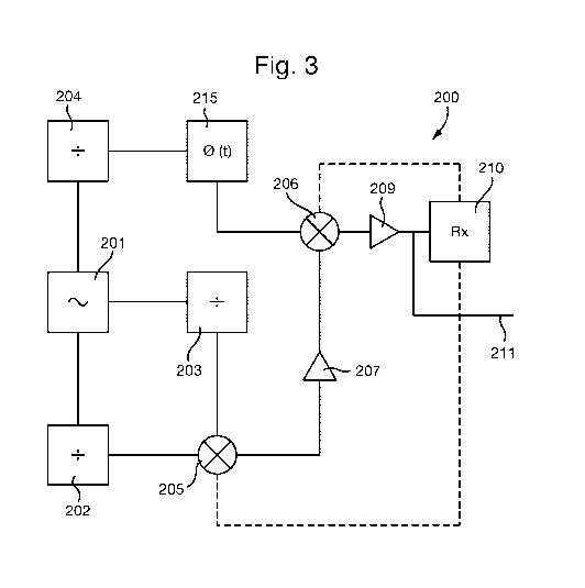
The variable frequency oscillator 102 is now described in detail. The variable
frequency oscillator 102 is provided by a variable frequency oscillator
circuit 200 as
shown in Figure 3. The variable frequency oscillator circuit 200 comprises a
fixed
frequency oscillator 201. The output of the fixed frequency oscillator 201 is
received
by frequency dividers 202, 203 and 204, each of which generates a divided
signal
from the signal from the fixed frequency oscillator.
The outputs of the frequency dividers 202 and 203 are passed to an image-
reject mixer 205, which is IQ-based, i.e. arranged to accept in-phase and a
quadrature signals. The signal from the frequency divider 203 is passed to the
mixer
205 as the local oscillator (LO) signal (and so split using a quadrature
splitter), while
the signal from the frequency dividers 202 is passed to the mixer 205 as the
intermediate frequency (IF) signal (and so split using a signal splitter). The
output of
the mixer 205 is then passed to an amplifier 207.
The output of the frequency divider 204 is passed to a modulator 215, which
can modulate the signal as described below. The output of the modulator 215 is
passed to an image-reject mixer 206, which again is IQ-based, as the IF
signal. The
output of the amplifier 207 is also passed to the mixer 206, as the LO signal.
CA 03045935 2019-06-03
WO 2018/109444
PCT/GB2017/053701
- 11 -
The output of the mixer 206 is then passed to an amplifier 209, and the
output of the amplifier provides the oscillating signal 211 of the desired
frequency.
The frequency dividers 202, 203 and 204 divide the signal from the fixed
frequency
oscillator 201 as required to provide the desired frequency for the
oscillating signal
211. For example, the frequency divider 202 may divide the frequency by 4 or
8, or
may simply provide a fixed DC output. The frequency divider 203 may divide the
frequency by 1 (i.e. leave it as it is) or by 2. The frequency divider 204 may
divide the
frequency 4, 8, 16 or 32. However, it will be appreciated that many other
dividing
factors could be used as required, and need not be powers of 2, but could be
dividing by powers of 3 or any other desired number. It will also be
appreciated that
many other arrangements of frequency dividers and mixers could be used in
accordance with the invention, to provide a desired frequency oscillation
signal.
Thus, in different embodiments with different arrangements of dividers and
mixers,
it will be possible to generate different sets of discrete frequencies.
As mentioned above, the output of the mixer 206 (following amplification by
the amplifier 209) provides the oscillating signal 211 of the desired
frequency.
However, in particular due to unwanted variations in the characteristics of
the
analogue components of the mixers 205 and 206, there may be unwanted signals
in
the oscillating signal 211, for example due to leakage of an LO signal
directly to the
output of a mixer, or image frequencies from the IF signal. To suppress these,
the
output of the amplifier 209 is also passed to a digitising receiver 210. In
the present
embodiment the digitising receiver 210 is comprised in a MIMO, but in other
embodiments the digitising receiver is provided in other ways, or indeed may
be an
analogue receiver, for example.
The digitising receiver 210 monitors for energy in frequencies other than the
desired oscillation frequency, which will be caused by unwanted signals. These
unwanted signals may be caused in a number of ways, for example by unwanted
variations in the characteristics of the components of the mixers 205 and 206.
To
suppress the unwanted signals, the variable frequency oscillator circuit 200
uses the
CA 03045935 2019-06-03
WO 2018/109444
PCT/GB2017/053701
- 12 -
results obtained by the digitising receiver 210 to modify the operation of the
mixers
205 and 206, as described below.
In one embodiment, in a calibration phase the oscillating signal 211 is
monitored, and used to determine calibration values that are used to modify
the
operation of the mixers 205 and 206, to suppress the unwanted signals. In
another
embodiment, during operation it is determined from the digitising receiver 210
that
leakage of the LO signal directly across the mixer 205 is occurring. To
suppress the
resulting unwanted signals, the DC offset (i.e. the relative DC levels) of the
in-phase
and quadrature inputs to the mixer 205 (and/or mixer 206 if appropriate) are
modified. In yet another embodiment, during operation it is determined that
there
are image frequency signals in the output of the mixer 205. To suppress the
unwanted image frequency signals, the amplitude and/or phase of the in-phase
and
quadrature inputs to the mixer 205 (and again and/or mixer 206 if appropriate)
are
modified. In another embodiment, modifications to the mixers 205 and/or 206
and/or modifications to the inputs to the mixers 205 and/or 206 are stored and
may
be recalled when returning to a desired oscillating frequency. In each case,
the
oscillating signal 211 continues to be monitored until the required
modification has
been achieved.
It will be appreciated that in other embodiments, a combination of some or
all of the above techniques, and/or other appropriate techniques, may be used.
As mentioned above, the variable frequency oscillator circuit 200 comprises a
modulator 215. This can be used in a particularly advantageous fashion to
modulate
the phase and/or amplitude of the oscillating signal 211. In particular, by
applying a
constant rate of change of phase, the modulator 215 will have the effect of
offsetting
the frequency. The unwanted effects of the modulation made can be adjusted for
by
the digital processing circuit 108 of the superhet receiver circuit 100, as it
can be fed
details of the modulation performed by the modulator 215, and so will be able
to
adjust for any disadvantageous effects the modulation would otherwise cause.
However, by for example sweeping the frequency across a small frequency range,
the digital processing circuit 108 will be more able to identify and eliminate
CA 03045935 2019-06-03
WO 2018/109444
PCT/GB2017/053701
- 13 -
unwanted signals, which might otherwise be impossible to identify from the
digitised
signals.
It will however be appreciated that in other embodiments of the invention,
the variable frequency oscillator circuit need not comprise such a modulator.
It will
.. also be appreciated that in other embodiments, the superhet receiver
circuit could
be implemented with a different variable frequency oscillator, for example a
standard known variable frequency oscillator. Further, it will also be
appreciated that
the variable frequency oscillator discussed above could be used in circuits
other than
a superhet receiver circuit.
While the present invention has been described and illustrated with
reference to particular embodiments, it will be appreciated by those of
ordinary skill
in the art that the invention lends itself to many different variations not
specifically
illustrated herein.
Where in the foregoing description, integers or elements are mentioned
which have known, obvious or foreseeable equivalents, then such equivalents
are
herein incorporated as if individually set forth. Reference should be made to
the
claims for determining the true scope of the present invention, which should
be
construed so as to encompass any such equivalents. It will also be appreciated
by
the reader that integers or features of the invention that are described as
preferable,
advantageous, convenient or the like are optional and do not limit the scope
of the
independent claims. Moreover, it is to be understood that such optional
integers or
features, whilst of possible benefit in some embodiments of the invention, may
not
be desirable, and may therefore be absent, in other embodiments.