Note : Les descriptions sont présentées dans la langue officielle dans laquelle elles ont été soumises.
CA 03048943 2019-06-28
WO 2018/121903 PCT/EP2017/077624
1
AN ASSEMBLY COMPRISING A NOISE EMITTING ELEMENT
The present invention relates to an assembly comprising an element for
emitting wireless
noise, such as an element for blocking communication with an NFC/RFID terminal
to prevent
undesired outputting of information from another element, such as a standard,
wireless
RFID/ID/NFC/payment card, item, token or the like, which is provided to always
respond to a
seemingly valid request with information which is not desired output to e.g.
criminals.
Blocking technology may be seen in W02005/052846, U52006/187046,
U52005/240778,
W02014/171955, W093/05489, U52008/0166962, EP899682 or 3P2004/151968.
A first aspect of the invention relates to an assembly of:
a first wireless communication element comprising:
- a first antenna configured to receive a wireless signal and output an
output
voltage,
- a first circuit connected to the first antenna and being configured to,
when
receiving the output voltage, output an output signal to the first antenna,
and
a second wireless communication element comprising:
- a second antenna configured to receive the wireless signal and output a
first
voltage,
- a voltage increasing element connected to the second antenna, the voltage
increasing element being configured to increase the first voltage by a
predetermined factor to
a second voltage and output the second voltage,
- a second circuit connected to the voltage increasing element and being
configured to, when receiving the second voltage, output a noise signal to the
second
antenna,
wherein:
.- the first circuit is configured to start outputting the output signal
when the
output voltage reaches a first threshold voltage,
CA 03048943 2019-06-28
WO 2018/121903 PCT/EP2017/077624
2
- the second circuit is configured to start outputting the noise signal
when the
second voltage reaches a second threshold voltage and
- the first threshold voltage exceeds the second threshold voltage divided
by the
predetermined factor.
In the present context, the first wireless communication element may be any
type of wireless
communication element configured to output a signal representing predetermined
and/or
useful, private, secret, account, identity, access data or the like. The first
wireless
communication element may be a standard RFID/NFC element, such as an access
card/dongle, identity card, credit/debit/purse card, travel card, loyalty card
(for use in gas
stations, super markets, shops or the like), or the like. However, also other
types of
elements, such as wireless car keys or a passport may be embodied as the first
wireless
communication element. Such elements may have the dimensions of a credit card
and often
are carried on a person, such as in a pocket and/or in a wallet and/or
bag/purse. This card or
dongle being wireless, it may not need to be removed from the person's
pocket/wallet/bag/purse. The mere proximity of the person and thus the first
wireless
communication element may have the first wireless communication element
respond to a
wireless signal by outputting another wireless signal related to the output
signal. The
terminal or the like receiving that wireless signal would then perform the
action desired, such
as opening/unlocking a door, facilitating a payment, checking in at a train
station,
unlocking/starting a car, or the like.
The operation of the first wireless communication element may be automatic.
Thus, when the
first antenna receives a wireless signal, the output voltage may automatically
be fed to the
first circuit which then, when this voltage is sufficient to power the
operation of the first
circuit, such as when the output voltage exceeds the first threshold voltage,
will output the
output signal to the first antenna which will then automatically output a
corresponding
wireless signal.
Often, the first circuit will, in addition to the output voltage received for
powering the
operation of the first circuit, derive a signal from the output voltage or
from another signal
received from the first antenna. This signal may identify a terminal or a
terminal type having
output the wireless signal. This identity may be derived from information
contained in the
wireless signal and/or a protocol to which the signal conforms. The protocol
may relate to a
signal frequency, signal type, encoding type or the like. The first circuit
may be configured to
output the output signal only when the wireless signal conforms to particular
requirements,
such as protocol and/or information embedded in the wireless signal under the
protocol.
CA 03048943 2019-06-28
WO 2018/121903 PCT/EP2017/077624
3
Also, the wireless signal output by the first wireless communication element
corresponding to
the output signal may be encoded, or the like, to conform to a predetermined
protocol.
Often, a protocol will specify the frequencies and the like of the wireless
communication
and/or signal fed to a wireless communication element and that from the
wireless
communication element.
However, such protocols and information are well-known also to fraudulent
persons, and the
manufacturing of a false terminal outputting the same information is well
within the grasp of
fraudulent persons.
In the present context, the second wireless communication element may be
shaped as the
first communication element, such as as a credit card shaped element,
preferably smaller and
thinner.
Both communication elements preferably are self powered in the sense that the
power
needed for operation is derived from the wireless signal received.
The operation of the second wireless communication element is to output the
noise signal to
the second antenna to have the second antenna output a wireless signal
interrupting the
usual communication between a terminal and the first wireless communication
element,
which could be a RFID/NFC/ID/payment card or item, for example. Preferably,
the operation
of the first wireless communication element may be interrupted or prevented,
so that this
communication may only take place if actually desired by a person, such as a
user or owner
of the first wireless communication element.
Preferably, the default operation of the second wireless communication element
is to output
the noise signal when receiving the wireless signal, so as to prevent the
first wireless
communication element from communicating at a point in time where the
user/owner does
not want such communication.
Thus, the operation of the second wireless communication may be automatic.
Thus, when the
wireless signal is received by the second antenna, the first voltage is
automatically fed to the
voltage increasing element automatically generating the second voltage and
feeding the
second voltage to the second circuit which automatically, such as when the
second voltage
reaches the second threshold voltage, outputs the noise signal to the antenna
which then
automatically outputs a corresponding wireless noise signal.
In general, an antenna may be a conductor into which an electrical signal is
fed and
converted into a wireless signal, such as an RF signal. Also, a wireless
signal may be received
CA 03048943 2019-06-28
WO 2018/121903 PCT/EP2017/077624
4
by the antenna and converted into an electrical signal. Often, an antenna is
shaped as a coil
with a number of windings.
An antenna may be selected to have particular electrical properties, such as a
desired
inductance, in order to obtain a desired resonance frequency together with a
circuit
connected to the antenna. Often, the resonance frequency is selected to be at
or around a
desired frequency, such as a frequency of signals to be received and/or
signals to be output.
When an antenna receives a wireless signal, power is output from the antenna.
This power
will have a voltage - the first voltage or the output voltage. In addition,
often the wireless
signal will comprise information or data, such as data indicating an identity
of the terminal.
This information/data may be present as a modulation of the voltage.
Naturally, the
modulation may be defined by a protocol, such as a packet protocol defining
how
predetermined information is encoded in the wireless signal. The information
may be as
simple as a frequency of the wireless signal.
The wireless signal may be output by a terminal as is usual in
RFID/NFC/ID/payment card
systems where a terminal will output a request RF signal to which neighbouring
RFID/NFC/ID
items/tokens/payment cards are to respond to in order to initiate a
communication resulting
in an identification, payment or the like, depending on what the targeted item
or token is
adapted for.
However, criminals may use concealed terminals to receive such information
from
ID/RFID/NFC payment cards/items in order to receive the response therefrom so
as to later
on "re-play" the same response to a legitimate terminal and thus emulate the
card/item from
which the information was derived. This is to be prevented.
Naturally, the voltage output by an antenna may vary over time. Often, when a
signal is
received by an antenna, the voltage output of the antenna will build up. Also,
the signal
strength of the wireless signal may vary, which of course will also affect the
voltage output of
the antenna. Finally, the voltage will also depend on what is connected to the
antenna. A
capacitor may be charged by the antenna, whereby the voltage output of the
antenna will
also depend on the charging state of such a capacitor.
A voltage increasing element is an element receiving one voltage and
outputting a higher
voltage. The voltage increase is by a predetermined factor exceeding 1.
Naturally, a current
output of the voltage increasing element may be lower than one received from
the antenna.
This, however is less of a problem when, which is usually the case, the second
circuit
primarily starts operation when the voltage fed reaches the second threshold
voltage. Using
CA 03048943 2019-06-28
WO 2018/121903 PCT/EP2017/077624
this element thus will make the second circuit start earlier than if the first
voltage was
applied to it.
Many manners exist of increasing a voltage. A transformer may be used. Other
types of
useful circuits are charge pumps.
5 The voltage increase may be selected based on a number of parameters,
such as the current
available. Naturally, the second circuit will need some current, and the
voltage increase may
cause the current output of the voltage increasing element to drop
correspondingly. Thus, in
one situation, the voltage increase may be controlled by a minimum current
output thereof to
the second circuit. This control may be real-time, programmable and/or be a
fixed value.
.. The voltage increase may be selected so that the second voltage is 1.1 or
more times the
first voltage (i.e. the factor is 1.1), such as 1.2 or more, 1.5 or more, 1.7
or more, 2 or
more, 2.5 or more or the like.
A circuit, such as the first and/or second circuit, may be any type of
circuit, monolithic or not.
The circuit may comprise an ASIC, controller, DSP, FPGA, processor or the like
or be made of
discrete components - or a combination thereof. Preferably, the circuit has an
energy
storage, such as a capacitor, receiving power, such as the output voltage or
the second
voltage and feeding the remainder of the circuit to allow it to output the
output signal or the
noise signal, respectively. Often, the antenna cannot receive a wireless
signal and thus
output the first/output voltage while receiving the noise/output signal. Thus,
power is
.. preferably first stored in order to operate the circuit when later
outputting the noise/output
signal.
The noise signal may be fed directly from the second circuit to the second
antenna or via e.g.
the voltage increasing element.
In the present context, a noise signal may be a signal which disturbs the
communication
between e.g. a terminal outputting the wireless signal and the first
communication element.
Thus, the noise signal may have a frequency component in a frequency band of
the wireless
signal and/or the desired frequency band of the output voltage and/or a
response from the
first communication element. The noise signal may be analogue or digital.
In a preferred embodiment, the wireless signal has a frequency of 105.9kHz and
the
.. response (such as the output voltage) from the first communication element
has a frequency
of 847.5kHz. Naturally, any frequency may be selected, such as any RF
frequency. Different
frequencies are used in different protocols.
CA 03048943 2019-06-28
WO 2018/121903 PCT/EP2017/077624
6
The noise signal may simply be a periodic signal having a frequency or a
frequency
component at a desired frequency.
In one situation, this wireless signal output from the second antenna is
output at the same
time as the wireless signal from the terminal and within the same frequency
interval, so that
the first communication element may not understand the signal from the
terminal and thus
not reply thereto.
In another situation, the wireless noise signal is output at the same time as
a reply from the
first communication element and within the same frequency range, so that the
terminal will
not be able to discern the contents of the signal from the first communication
element. Thus,
the combined signal received by the terminal, if any signal is output by the
first
communication element, may be scrambled to a degree where any information
comprised in
the signal output of the first communication element may not be derivable.
Preferably, however, the noise signal is output at the same time as the
wireless signal from
e.g. a terminal so that the receiving first communication element is not able
to discern and
.. decode it correctly. In that situation, the first communication element
will not output a
response at all. Then, the secret information of such a response is not
revealed.
The outputting of the noise signal may result in a short circuiting of another
wireless signal.
Thus, the outputting of the noise signal may short circuit the wireless signal
from the
terminal so that other antennas in the vicinity of the second antenna, such as
the first
antenna, do not see, or do not sufficiently see, the wireless signal from the
terminal.
In one embodiment, the noise signal is a square signal. An advantage of a
square signal is
that sharp edges cause the signal emitted by the second antenna to have
harmonics
extending to other frequencies than the main frequency of the square signal.
Thus, noise
may be output over an extended frequency range or in a frequency range outside
of the main
frequency of the square signal. Thus, if the second circuit for example is not
able to operate
at a sufficiently high frequency, the use of square pulses may nevertheless
output noise at a
desired, higher frequency.
In this context, a square pulse or signal is a signal with sufficiently sharp
edges. Preferably,
the rise or fall time from maximum to minimum takes place in less than 10%,
such as less
than 5%, such as less than 1% such as less than 0.5% of the total period of
the signal.
Often, the noise signal is a periodic signal with a duty cycle of 50% or less.
In digital signals,
the duty cycle is the percentage of a period where the signal is "1" or
"high". As will be
CA 03048943 2019-06-28
WO 2018/121903 PCT/EP2017/077624
7
described below, a lower duty cycle will make the pulses more narrow, causing
more
harmonics at higher frequencies. Thus, the duty cycle may be selected together
with the
frequency or period of the noise signal in order to obtain a desired wireless
signal output at a
given frequency.
Another factor to take into account by the duty cycle is that when the signal
output is a
binary "0", no signal is output, and the wireless signal may be received by
the second
antenna, so that the first and therefore the second voltage may be output.
Thus, power may
be collected for use by the second circuit for outputting the next "1" of the
next period of the
noise signal.
In one situation, the noise signal comprises a number of pulses, where a width
of a pulse is
3p5 or less, such as 2p or less, such as 1-2p5. When sufficiently narrow
pulses are used,
noise is output in frequency bands at multiples (harmonics) of the frequency
of the noise
signal.
Presently, 1.4p5 pulses are preferred with a duty cycle of 16.7%.
In one situation, a frequency of the noise signal is at least 50% of a
predetermined
frequency, and wherein the duty cycle is at least 30%. Thus, when the noise
signal has a
frequency at or close to the desired frequency, a larger duty cycle may be
used, as noise
may not be needed at higher harmonics. In fact when outputting a noise signal
at the
frequency of interest, the noise signal need not be square-shaped.
In another situation, where a frequency of the noise signal is less than 50%
of a
predetermined frequency, the duty cycle preferably is no more than 30%. In
that situation,
narrower pulses may be desired in order to obtain a wireless noise signal
having higher
harmonics, such as at frequencies at or near the predetermined frequency.
The purpose of the voltage increasing element is to generate the second
voltage which
makes the second circuit start outputting the noise signal, before the first
circuit starts
outputting the output signal.
The first and second circuits are each configured to start outputting the
respective
output/noise signal when the output/second voltage reaches the first/second
threshold
voltage, respectively,
CA 03048943 2019-06-28
WO 2018/121903 PCT/EP2017/077624
8
Often, antennas for the same communication type (protocol and/or frequency)
have
approximately the same parameters, so that they often output comparable
voltages when
receiving a wireless signal (where signal strength of the wireless is the
same).
However, often the first and second threshold values are not the same. The
threshold value
of a circuit depends on a number of factors, such as the production method and
the like.
Then, when the first threshold voltage exceeds the second threshold voltage
divided by the
predetermined factor, the second circuit will start operating or at least
start outputting the
noise signal before the first circuit starts operating and/or starts
outputting the output signal.
This may be determined by providing each of the first and second communication
elements
at a predetermined distance from a terminal and determining the period of time
passing
between the outputting of the wireless signal to the outputting of the output
signal or noise
signal - or the period of time lapsing from the first/second antenna receiving
the wireless
signal and to the outputting of the output signal or the noise signal.
The elements may be tested individually. It is noted that the outputting of
the noise signal
may additionally interfere with the outputting of the output signal, as the
second antenna,
when receiving the wireless signal, will have a tendency of at least absorbing
part of the
energy in the wireless signal. This will delay the point in time at which the
first circuit can
start, as the signal strength and thus the output voltage, will be lower.
Also, if the outputting of the noise signal is intended to interfere with the
reception or
interpretation of the wireless signal in the first circuit, the outputting of
the noise signal may
also in that manner interfere with the outputting of the output signal from
the first circuit, as
it may altogether prevent the first circuit from outputting the output signal
even when
operating.
In one embodiment, the second wireless communication element further comprises
a voltage
limiting element configured to limit the second voltage to a voltage not
exceeding a
predetermined maximum voltage. Some circuits are not able to handle voltages
exceeding a
maximum voltage. However, when the first voltage is high, such as if a
distance to a terminal
outputting the wireless signal is low, the second voltage may exceed this
maximum voltage,
which could then damage the second circuit. This may be avoided by adding a
limiting
element. A limiting element may be as simple as a diode, for example.
Naturally, the first wireless communication element may also have a voltage
increasing
element. In this situation, the first circuit would also start outputting of
the output signal at
CA 03048943 2019-06-28
WO 2018/121903 PCT/EP2017/077624
9
an earlier point in time compared to if simply supplied by the voltage
directly from the first
antenna. In this situation, the voltage increases of the voltage increasing
elements of the
first and second communication elements may be adapted to each other so as to
ensure that
the second circuit still starts before the first circuit - at least when the
same wireless signal is
received by the two antennas at the same time, such as if the first and second
communication elements are positioned beside each other and thus with the same
distance
to the terminal.
When an electrical signal is fed to an antenna, a corresponding wireless
signal will be output
from the antenna in the same manner as a wireless signal received by an
antenna will
generate a corresponding voltage in the antenna. In this context,
"corresponding to" will
mean that e.g. a frequency present in the wireless signal will also be present
in the signal
output to/fed to the antenna. Thus, if the wireless signal is modulated, the
modulation
frequency may also be seen in the signal from the antenna.
In a preferred embodiment, the voltage increasing element has a first and a
second terminal,
a first, a second and a third capacitor and a first and a second diode, where:
- the second and third capacitors are connected in series between a first
voltage
and a first conductor,
- the first and second diodes are connected in series between the first
voltage
and the first conductor,
- the first capacitor is connected between the first voltage and the first
conductor,
- the first capacitor is configured to feed the second voltage from the
first
capacitor to the circuit,
- a terminal of the antenna is connected between the second and third
capacitors
and
- another terminal of the antenna is connected between the first and second
diodes.
Preferably, the diodes are both directed to guide current from the first
voltage, which may be
ground, toward the first conductor.
CA 03048943 2019-06-28
WO 2018/121903 PCT/EP2017/077624
The first conductor may be connected to a power input of the circuit.
In one embodiment, the circuit is configured to output as the noise signal a
square signal.
In one embodiment, the noise signal comprises a number of pulses, where a
width of a pulse
is 3p5 or less, such as 2p or less, such as 1-2p5.
5 .. In one embodiment, the noise signal is a periodic signal with a duty
cycle of 50% or less.
In one embodiment, a frequency of the noise signal is at least 50% of a
predetermined
frequency, and wherein the duty cycle is at least 30%.
In another embodiment, a frequency of the noise signal is no more than 50% of
a
predetermined frequency, and wherein the duty cycle is no more than 30%.
10 .. In one embodiment, the first and second wireless communication elements
have the same
overall shape, such as a shape resembling a credit card or a dongle/fob/tag to
be attached to
e.g. a key chain. Then, the first and second elements may be carried or
transported together,
such as in a key chain or in a wallet, so that the second element is carried
together with the
first element in order to be able to carry out its operation and thus protect
the information in
the first element. Ultimately, the first and second wireless communication
elements may be
built into the same element, such as a credit card shaped element, a pass
port, key fob or
the like.
Naturally, sometimes the output signal of the first element is actually
desired converted into
a wireless signal to be received by a terminal. In that situation, the second
circuit may be
disabled, such as by preventing the second voltage from feeding the circuit,
by reducing the
voltage fed to a lower voltage, by preventing the noise signal from reaching
the second
antenna, or the like. This disabling may be user initiated such as by
operating a switch or
other operable element.
Another aspect of the invention relates to a method of operating an assembly,
such as an
assembly according to the first aspect of the invention, comprising:
- a first wireless communication element comprising a first antenna and a
first circuit
and
- a second wireless communication element comprising a second antenna, a
voltage
increasing element and a second circuit,
CA 03048943 2019-06-28
WO 2018/121903
PCT/EP2017/077624
11
the method comprising the steps of:
1. an emitter outputting a wireless signal,
2. the first and second antennas receiving the wireless signal and outputting
an output
voltage and a first voltage, respectively,
3. the voltage increasing element receiving the first voltage and outputting a
second
voltage, the second voltage being larger than the first voltage and
4. the first and second circuits receiving the output voltage and the second
voltage,
respectively, and outputting an output signal and a noise signal,
respectively, to the
first and second antennas, respectively,
where the second circuit starts outputting the noise signal before the first
circuit starts
outputting the output signal.
This may be the situation where the main function of the noise signal is to
scramble the
signal output from the first element.
A third aspect of the invention relates to a method of operating an assembly,
such as an
.. assembly according to the first aspect of the invention, comprising:
- a first wireless communication element comprising a first antenna and a
first circuit
and
- a second wireless communication element comprising a second antenna, a
voltage
increasing element and a second circuit,
the method comprising the steps of:
1. an emitter outputting a wireless signal,
2. the first and second antennas receiving the wireless signal and outputting
an output
voltage and a first voltage, respectively,
3. the voltage increasing element receiving the first voltage and outputting a
second
voltage, the second voltage being larger than the first voltage and
4. the first and second circuits receiving the output voltage and the second
voltage,
respectively,
5. the second circuit outputting a noise signal to the second antenna, without
the first
circuit outputting an output signal to the first antenna.
This may be the situation where the operation of the second element is to
output a signal
interfering with the wireless signal from the terminal so that the first
circuit does not output
CA 03048943 2019-06-28
WO 2018/121903 PCT/EP2017/077624
12
any output signal as it cannot ascertain that the wireless signal from the
terminal conforms
to a desired protocol.
Naturally, the first, second and third aspects may be combined, and all
embodiments and
elements of the first aspect are equally valid in this respect.
In this context, an emitter outputting the wireless signal may be any type of
emitter, such as
a standard RFID/NFC terminal, such as that of a ATM, a door access system, a
payment
terminal, a mobile telephone, or other elements used for identifying or
recognizing a wireless
element or token, such as an ID card, access card, payment card, ticket, or
the like The
wireless signal may be a HF/UHF signal and/or a signal used in RFID and/or
NFC.
Preferably, step 2 comprises the first and second antennas receiving the
wireless signal at
the same time. Then, the first and second antennas and thus wireless
communication
elements may be at the same distance to the emitter for this determination.
Naturally, these
distances need not be identical. One of the first and second antennas may be
up to 10%
farther away from the emitter than the other, but preferably, the distances
are within 5%,
such as within 2% or 1% of the largest distance. This will make one antenna
receive the
wireless signal slightly before the other, but this may be taken into account
when
dimensioning or selecting the voltage increasing element. It is noted that the
power of the
wireless field reduces with the distance cubed, so a distance difference will
affect the voltage
output from the antenna more than the altered travelling time of the wireless
signal.
As described above, the operation and steps of the individual elements may be
automatic so
that when receiving the wireless signal, the generation of the voltage and the
output of the
signal is automatic, if the voltage is sufficient. Thus, the operation of the
noise signal is to
scramble or disturb the signal output of the first antenna.
The second circuit starts the outputting of the noise signal before the first
circuit starts
outputting the output signal. Thus, the second circuit may prevent the first
circuit from
outputting the signal altogether. It may suffice that the circuits start at
the same time, but it
may be desired to ensure that the noise signal is output first in order to
ensure that the
signal output of the first circuit is not comprehensible.
The controlling of the relative points in time of outputting may be a
controlling of the time
intervals required from an antenna receives the wireless signal and until the
signal is output
from the circuit. The voltage increase is a manner of starting a circuit
faster, as the circuits
often start operating when the voltage fed thereto exceeds a threshold value.
Thus, the
CA 03048943 2019-06-28
WO 2018/121903 PCT/EP2017/077624
13
voltage increase will ensure that the second circuit starts earlier than if
the voltage increase
was not performed.
The voltage increase then may be tailored or selected to ensure that the
second circuit starts
sufficiently early.
It is noted that the first circuit may also itself cause a delay in the
outputting of the output
signal, compared to the processing time required by the second circuit from
the start of
operation to the outputting of the noise signal. The first circuit may analyse
the output
voltage or information comprised therein to determine whether to output the
output signal at
all. The first circuit may compare the information of the voltage or other
information
derivable from the voltage to predetermined information to make the decision.
The first
circuit may determine whether the output voltage or information therein
conforms to a
predetermined protocol and output the output signal only if this protocol is
adhered to.
Thus the first circuit may itself decide to not output the output signal even
if receiving a
wireless signal, if the wireless signal adheres to a wrong protocol, such as
if the wireless
signal has a carrier frequency falling outside of a predetermined frequency
interval.
This analysis of the output voltage may delay the first circuit to a degree
where the second
circuit has started outputting the noise signal. This delay may be taken into
account when
dimensioning or selecting the voltage increase.
In one embodiment, the second voltage is at least 2 times the first voltage.
In one embodiment, the noise signal is a square signal and/or the noise signal
comprises a
number of pulses, where a width of a pulse is 3p5 or less.
In one embodiment, the noise signal is a periodic signal with a duty cycle of
50% or less.
In one embodiment:
- a frequency of the noise signal is at least 50% of a predetermined
frequency,
and wherein the duty cycle is at least 30% or
- a frequency of the noise signal is no more than 50% of a predetermined
frequency, and wherein the duty cycle is no more than 30%.
CA 03048943 2019-06-28
WO 2018/121903 PCT/EP2017/077624
14
In one embodiment, in step 2, the output voltage is no less than 90% of the
first voltage and
no more than 110% of the first voltage.
In one embodiment, step 4 comprises the step of limiting the second voltage to
a voltage not
exceeding a predetermined voltage before feeding the limited voltage to the
second circuit.
In the following, preferred embodiments of the invention will be described
with reference to
the drawing, wherein:
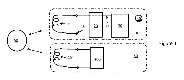
- Figure 1 illustrates a preferred embodiment according to the invention,
- Figure 2 illustrates an embodiment of the voltage increasing element.
In figure 1, an assembly is illustrated having a standard RFID/NFC card 60,
such as a credit
card or an ID card, having an antenna 15' and a circuit 200, and an element,
such as a thin,
credit card shaped element 10 which has an antenna 15 connected to a voltage
increasing
element 20 via terminals 16 and which is again connected to a noise generating
circuit 30 via
connections 17.
The antenna 15 may be a standard coil used for NFC or RF communication, such
as for RFID
communication or other wireless communication often used for identification,
payment or
similar purposes. The antenna 15' may be the same type of antenna or another
type of
antenna - but again may be a standard antenna type.
The circuit 200 is connected to the antenna 15' in the standard manner. When
receiving a
wireless signal from the reader 50, the antenna will output an output voltage
to the circuit,
which derives power from this signal and generates an output signal to the
antenna 15'. The
output signal usually comprises identity information and/or other sensitive
information for a
genuine or trustworthy reader 50 to receive.
However, fraudulent readers 50 may exist which will attempt to access this
output signal to
illegally use that information against the will of the owner. This is to be
avoided.
The circuit 30 may be connected to the element 20 only, or one terminal
thereof may be
connected directly to the coil if desired (hatched line).
The circuit 30 is configured to output, when powered, a noise signal (see
below) in order to
prevent or block communication between the RFID/NFC terminal 50 and the
RFID/NFC
element 60, which is also in the vicinity of the element 10.
CA 03048943 2019-06-28
WO 2018/121903 PCT/EP2017/077624
When the terminal 50 outputs its usual request signal, the antenna of the
element 10, as in
usual ID/payment cards, will receive the signal and output power and thus a
voltage. In
usual RFID/NFC elements, this power is fed to a chip 200 which then will
operate to respond
to the request signal with an identification of the RFID/NFC element. The
element 60 may be
5 a standard RFID/NFC element.
However, such responses may not always be desired, whereby blocking or
prevention of this
communication is desired. It is not practical to prevent the terminal 50 from
outputting the
signal, and in some situations, criminals will carry terminals in crowded
spaces, such as
trains, in order to obtain information from RFID/NFC elements 60. Thus, the
terminals 50 are
10 not controllable or trustworthy to the desired extent.
The present element 10, however, will, when sensing a signal from a terminal
50, itself
output a noise signal aimed at preventing near-by NFC/RFID elements 60, such
as ID or
payment cards, from either receiving or correctly interpreting the terminal
request signal (the
NFC/RFID elements usually only respond to a request signal complying to a
given standard or
15 protocol), or at outputting a signal scrambling any signal output by the
NFC/RFID elements
60.
As the energy obtainable from a request signal depends a lot on the distance
between the
terminal antenna and the antenna of the elements 10/60, it is highly desired
that the present
element 10, at least when positioned at the same distance to the terminal 50
as the element
60, is faster than the NFC/RFID element 60 in order to ensure that the
scrambling or noise
emitting starts so early that the NFC/RFID element 60 does not have time to
output its
response, before the noise signal is output.
The chip 30 will start operating when the voltage fed thereto reaches a
threshold voltage.
The voltage output of the coil 15 will increase, as the field is detected and
the power
collected increases. The operation of the voltage increasing element 15 is to
receive the
power and voltage output of the antenna 15 and increase the voltage and feed
this increased
voltage to the circuit 30. As a result thereof, the circuit 30 will start
operation earlier and
thus be faster to perform its preventing/blocking action compared to the
circuit 200 not
having this "voltage boost".
In some circumstances, however, it is actually desired to have the ID or
payment card 60
respond to a terminal request signal, such as when entering a secured door or
making a
payment. Thus, it is desired to be able to prevent the operation of the
circuit 30. To this
effect, a switch or other user operable element 40 may be provided. The user
may operate
this element 40 and thereby send a signal to the circuit 30 to not operate.
CA 03048943 2019-06-28
WO 2018/121903 PCT/EP2017/077624
16
The element 40 may be a standard switch, a wireless receiver for signals
output by e.g. a
mobile telephone of the user, or a piezo element outputting a voltage when
bent, so that the
user need only deform (or just tap) the element 10 to stop the noise
outputting operation.
The noise outputting operation may be carried out in many manners. In one
embodiment,
the noise outputting step comprises the outputting of sharp pulses, such as
square pulses.
The advantage of such sharp pulses or sharp corners is that these will
generate an output not
only at the frequency of the pulses but also at harmonics thereof. Thus, a
noise signal with a
wider spectrum may be output.
Usually, the request signal from the terminal 50 is 105.9kHz and the response
from a
RFID/ID/NFC card 60 is 847.5kHz. In principle, the noise signal may operate in
any of these
frequency bands.
In one situation, the noise signal has a frequency within 10% of one of the
above frequency
bands. However, it is also possible to provide a noise signal with a frequency
lower than one
of the frequency bands, especially if the pulse width of the signal is
reduced. Lower pulse
widths create more harmonics which therefore will also create noise at higher
frequencies.
Also, the duty cycle may be selected. It is noted that a low duty cycle
outputs the signal only
during a lower proportion of the period of the signal. In the remaining
portion of the period of
the signal, no signal is output, whereby power may be collected by the element
10 for
continued operation of the circuit 30.
Thus, a duty cycle of at least 30%, such as at least 40%, such as around 50%
may be
selected especially if the frequency of the noise signal is at or at least
within 20% or 10% of
the desired frequency, whereas a duty cycle of no more than 30%, such as no
more than
20%, such as no more than 15% may be desired, if the frequency of the
frequency to be
blocked is at least twice the frequency of the noise signal.
Figure 2 illustrates a preferred embodiment of the voltage increasing element
20. The
element is provided to the left of and at the top of the circuit 30. To the
right, the sensor 40
is illustrated, here in the form of a piezo element and a variable resistor in
addition to a
voltage divider all provided to protect the circuit 30 from the high voltage
potentially output
of the piezo.
The element 20 receives the signal from the terminals 16 and feeds the signal
from the upper
terminal (through a resistor) to the circuit 30. This signal is fed between
two diodes, D2 and
D3 provided between an output and ground.
CA 03048943 2019-06-28
WO 2018/121903 PCT/EP2017/077624
17
The signal from the lower terminal is fed between two capacitors, C2 and C3,
also provided
between ground and the output.
The operation of this set-up is that when the signal is positive on the upper
terminal and thus
negative on the lower terminal, D2 will be conducting while the diode D3 will
be blocking, so
the voltage across C2 will build up.
When, on the other hand, the signal is negative on the upper terminal and
positive on the
lower terminal, D3 will be conducting while the D2 will be off, so the voltage
across C3 will
build up.
The voltage output is fed to the capacitor Cl which holds the voltage fed to
the circuit 30 for
operation. A LED D1 is provided for protecting the circuit 30 from any
excessive voltage
output of the capacitor Cl. D1 may be dimensioned to be conducting at a
voltage close to the
max voltage for the circuit 30. D1 may of course be replaced by any other
circuit having the
same effect, such as a circuit disposing of the power by creating heat (a
resistor).
Ignoring the voltage drop in D2 and D3, the voltage across both C2 and C3 will
be that
received from the coil, i.e. the first voltage, V. Then, the voltage fed to
Cl, the second
voltage, is the voltage across C2 + the voltage across C3, i.e 2*V. This
circuit thus acts as a
voltage doubler.
When operating, the circuit 30 outputs the noise signal to the upper terminal
and thus to the
antenna.
The element 10 preferably is provided in the vicinity of the
RFID/ID/NFC/payment cards or
items to protect. The element 10 may be embodied as a thin element which may
be glue to a
wireless card, for example, to protect or to e.g. a wallet or other holder for
such cards.
Any voltage increase may be selected. As mentioned above, the voltage
increasing circuit
may be implemented in a number of manners, including in discrete components.
Some
examples are:
http://www.circuitstoday.com/voltage-doubler-circuit-using-ne555
http://www.electronics-tutorials.ws/blog/voltage-multiplier-circuit.html
CA 03048943 2019-06-28
WO 2018/121903 PCT/EP2017/077624
18
Naturally, the element 60 may also have a voltage increasing element as that
of the element
10. A reason for increasing the voltage fed to the circuit 200 may be to
increase the range
thereof. In this situation, the voltage increasing element 20 of the element
10 should be
adapted (or the threshold voltage of the circuit 30), so that the circuit 30
nevertheless will
reach its threshold voltage before the circuit 200 does.