Note : Les descriptions sont présentées dans la langue officielle dans laquelle elles ont été soumises.
20180104CA01
COATED PRINTED ELECTRONIC DEVICES EXHIBITING IMPROVED YIELD
[0001] Printed electronics based on memory cells are used in a wide
variety of
applications, including as labels, tags and sensors. The memory cells are
capacitor-like
structures, each structure including a layer of a memory material sandwiched
between a pair
of electrode layers. The memory cells may be accessed via conductive traces
linking the
electrodes to an electronic driver and detection circuitry which may be
located on the
periphery of the memory cells or in a separate module, e.g., a read/write
unit. Depending
upon the application, the printed electronic device may contain a few or up to
several million
memory cells. Regardless of the particular configuration of the printed
electronic device, the
yield of the device is generally maximized in order for the device to operate
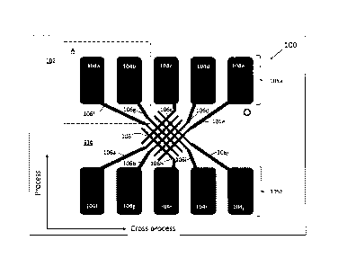
as intended (e.g.,
to allow for accurate and efficient reading of, and writing to, the individual
memory cells).
Unfortunately, despite the advantages of the various printing methods (e.g.,
inkjet printing,
screen printing, gravure printing, etc.) used to fabricate printed electronic
devices, many
factors in the fabrication process can contribute to reduced yield of the
devices.
[0002] Provided are coated printed electronic devices exhibiting improved
yield and
methods of fabricating and using such devices.
[0003] In embodiments coated, printed electronic devices are provided
which comprise a
plurality of contact pads arranged in a pattern, a plurality of electrode
traces arranged in
another pattern, the plurality of electrode traces comprising a set of bottom
electrode traces
and a set of top electrode traces, each electrode trace in electrical
communication with an
associated contact pad of the plurality of contact pads, a plurality of memory
cells, each
memory cell located at an intersection of a pair of electrode traces of the
plurality of electrode
traces and comprising a bottom electrode layer formed from a region of one of
the bottom
electrode traces, a top electrode layer formed from a region of one of the top
electrode traces,
and a ferroelectric layer between the bottom and top electrode layers, and a
protective layer
covering the plurality of electrode traces and extending laterally beyond each
edge of each
electrode trace to provide a buffer zone surrounding each electrode trace, the
buffer zone
extending from an end of each electrode trace to cover a portion of each
associated contact
pad in an overlapping region, wherein each contact pad also has at least one
uncovered edge.
[0004] In embodiments, methods of fabricating coated, printed electronic
devices are
provided which comprise printing a plurality of bottom electrode traces on a
substrate;
1
Date Recue/Date Received 2020-12-24
20180104CA01
printing a layer of a ferroelectric material on the plurality of bottom
electrode traces; printing
a plurality of top electrode traces on the layer of the ferroelectric
material, wherein the
plurality of bottom and top electrode traces forms a plurality of electrode
traces arranged in a
pattern and defines a plurality of memory cells, each memory cell located at
an intersection of
a pair of electrode traces of the plurality of electrode traces; printing a
plurality of contact
pads on the plurality of electrode traces, wherein the plurality of contact
pads is arranged in
another pattern and each electrode trace of the plurality of electrode traces
is in electrical
communication with an associated contact pad of the plurality of contact pads;
printing a
curable composition on the plurality of electrode traces and the plurality of
contact pads; and
curing the curable composition to form a protective layer. The protective
layer covers the
plurality of electrode traces and extends laterally beyond each edge of each
electrode trace to
provide a buffer zone surrounding each electrode trace, the buffer zone
extending from an
end of each electrode trace to cover a portion of each associated contact pad
in an
overlapping region, wherein each contact pad also has at least one uncovered
edge.
[0005] In embodiments, methods of using coated, printed electronic devices
are provided
which comprise contacting a plurality of contact pads of a coated, printed
electronic device
with a plurality of pins of a read/write unit, the device comprising the
plurality of contact
pads arranged in a pattern, a plurality of electrode traces arranged in
another pattern, the
plurality of electrode traces comprising a set of bottom electrode traces and
a set of top
electrode traces, each electrode trace in electrical communication with an
associated contact
pad of the plurality of contact pads, a plurality of memory cells, each memory
cell located at
an intersection of a pair of electrode traces of the plurality of electrode
traces and comprising
a bottom electrode layer formed from a region of one of the bottom electrode
traces, a top
electrode layer formed from a region of one of the top electrode traces, and a
ferroelectric
layer between the bottom and top electrode layers, and a protective layer
covering the
plurality of electrode traces and extending laterally beyond each edge of each
electrode trace
to provide a buffer zone surrounding each electrode trace, the buffer zone
extending from an
end of each electrode trace to cover a portion of each associated contact pad
in an
overlapping region, wherein each contact pad also has at least one uncovered
edge.
[0006] FIG. 1A depicts a top view of a coated printed electronic device
according to an
illustrative embodiment. FIG. 1B depicts an expanded view of section A of the
coated printed
electronic device of FIG. 1A. FIG. 1C depicts a cross-sectional view of a
memory cell of the
coated printed electronic device of FIG. 1A.
2
Date Recue/Date Received 2020-12-24
20180104CA01
[0007] FIG. 2 depicts a top view of a comparative coated printed
electronic device.
[0008] FIG. 3 depicts a top view of a coated printed electronic device
according to an
illustrative embodiment.
[0009] FIG. 4 depicts a top view of the coated printed electronic device
of FIG. 1A, but
in which the protective layer has been darkened to show its lateral dimensions
more clearly.
[0010] FIG. 5 depicts a top view of the coated printed electronic device
of FIG. 3, but in
which the protective layer has been darkened to show its lateral dimensions
more clearly.
[0011] Provided are coated printed electronic devices exhibiting improved
yield and
methods of fabricating and using such devices.
[0012] The coated printed electronic devices are based on arrays or
matrices of memory
cells known as passive arrays or matrices. The devices are multilayer
structures comprising
stacked layers, each layer composed of a different material and/or configured
in a different
pattern, depending upon the function of the layer. The devices comprise a
plurality of contact
pads arranged in a pattern; a plurality of electrode traces arranged in
another pattern, the
plurality of electrode traces comprising a set of bottom electrode traces and
a set of top
electrode traces, each electrode trace in electrical communication with an
associated contact
pad of the plurality of contact pads; a plurality of memory cells, each memory
cell located at
an intersection of a pair of electrode traces of the plurality of electrode
traces; and a
protective layer covering the plurality of electrode traces. Each memory cell
comprises a
bottom electrode layer, a top electrode layer, and a ferroelectric layer
between the top and
bottom electrode layers. The top and bottom electrode layers of the memory
cells correspond
to regions of top and bottom electrode traces, respectively. Moving from
bottom to top in the
devices, the set of bottom electrode traces is one of the layers of the
multilayer structure, the
ferroelectric layer is a layer overlying the set of bottom electrode traces,
the set of top
electrode traces is a layer overlying the ferroelectric layer, the plurality
of contact pads is a
layer overlying the set of top electrode traces and the protective layer is a
layer overlying the
plurality of contact pads. The protective layer may be the topmost layer in
the device.
[0013] The protective layer protects the underlying layers of the coated
printed electronic
devices from a variety of external forces which can damage the devices, e.g.,
scratches,
abrasion, chemicals, etc. Conventionally, coverage of the protective layer
over the underlying
material layers has been maximized so as to maximize the level of protection
for these
underlying material layers. The present disclosure is based, in part, on the
finding that the
3
Date Recue/Date Received 2020-12-24
20180104CA01
yield of coated printed electronic devices is improved (i.e., increased) when
using protective
layers that provide reduced coverage as compared to conventional coated
printed electronic
devices. This is surprising since the protective layers themselves are not the
electrically active
components of the printed electronic devices and so would otherwise be thought
to have a
minimal effect on yield. The increased yield is further described below with
respect to
illustrative embodiments of coated printed electronic devices (see FIGs. 1A
and 3). Reduction
of the coverage of the protective layer also has the advantage of reducing
costs since less
material is used.
[0014] In the present coated printed electronic devices, the protective
layer covers the
underlying plurality of electrode traces. From a top view of the device (e.g.,
see FIGs. 1A and
3), this means the lateral (i.e., in plane) dimensions of the protective layer
at least match the
lateral dimensions of each of the electrode traces of the plurality of
electrode traces which
underlie the protective layer. However, the protective layer also covers,
i.e., extends laterally
over, a region beyond edges of each electrode trace of the plurality of
electrode traces. This
extended region fully surrounds each electrode trace and is referred to herein
as a "buffer
zone." The buffer zone may be characterized by a width corresponding to the
distance
between an edge of a covered electrode trace to an edge of the protective
layer, the width
measured along an axis perpendicular to the longitudinal axis of the electrode
trace. At an end
of an electrode trace, the buffer zone can extend radially from each corner of
the electrode
trace a distance equivalent to the buffer zone width. Thus, the buffer zone
effectively traces
the perimeters of, and thus, surrounds, each electrode trace of the plurality
of electrode traces.
The buffer zone width, i.e., the amount of lateral extension beyond the edges
of each
electrode trace, is at least 2 * * (line registration capability) . By
"line registration
capability" it is meant the registration error value associated with the
printing apparatus used
to print the protective layer. The registration error value for a printing
apparatus may be
provided by the manufacturer of the printing apparatus or may be determined by
monitoring
printed registration marks against a fixed datum to which all printed layers
are registered
against At least in some lateral locations (i.e., locations within the plane
of the protective
layer), the buffer zone width is greater than 2 * * (line registration
capability).
[0015] Because the protective layer extends laterally beyond the edges of
each of the
electrode traces of the plurality of electrode traces and since each electrode
trace is in direct
contact with an associated contact pad, a portion of each contact pad of the
plurality of
4
Date Recue/Date Received 2020-12-24
20180104CA01
contact pads is also covered by the protective layer, i.e., the protective
layer overlaps onto
each contact pad. The region of a contact pad covered by the protective layer
may be referred
to herein as an overlapping region. However, in such overlapping regions, the
buffer zone
width is no more than 2 * -\/7 * (line registration capability) . That is,
although the buffer
zone width may be more than 2 * -\/7 * (line registration capability) in some
lateral
locations in the protective layer, in the overlapping regions, the buffer zone
width is no more
than 2 * -\/7 * (line registration capability). In embodiments, the buffer
zone width is 2 *
* (line registration capability) in the overlapping regions. In embodiments,
the buffer
zone width in the overlapping regions is greater than zero but no more than
500 !um; greater
than zero but no more than 400 [tm; or greater than zero but no more than 300
p.m. In
embodiments, the buffer zone width in the overlapping regions is in a range of
greater than
200 vim to 2 * -\/7 * (line registration capability). In embodiments, the
buffer zone width
in the overlapping regions is in a range of greater than 200 pm to 500 pm.
This includes
buffer zone widths of 2501.1m, 275 pm, 300 vim, 325 ttm, and 350 vim. In the
design phase,
distances may be calculated using CAD software. Post production, these
distances may be
measured with a video measurement system.
[0016] Although the protective layer overlaps a portion of each contact
pad of the
plurality of contact pads, each contact pad also has an uncovered portion,
i.e., a portion over
which the protective layer does not overlap. In embodiments, each contact pad
is covered by
the protective layer in an overlapping region and has a remaining portion
which is uncovered,
i.e., the rest of the contact pad is not covered by the protective layer. This
is useful to
minimize the wicking of the material of the protective layer onto the material
of the contact
pad.
[0017] Each contact pad of the plurality of contact pads may also have at
least one edge
which is uncovered by the protective layer, i.e., at least one edge which the
protective layer
does not contact and does not overlap. In embodiments, all edges of each
contact pad are
uncovered by the protective layer, except for those covered due to the buffer
zone/overlapping region. In embodiments, the protective layer is further
configured to define
a gap between an edge of the protective layer and an adjacent, facing edge of
each contact
pad. The gap may be characterized by a width corresponding to the distance
between the edge
of the protective layer and the adjacent, facing edge of the contact pad,
measured along an
axis perpendicular to the edges. In embodiments, the gap width is at least 2 *
5
Date Recue/Date Received 2020-12-24
20180104CA01
(line registration capability). In embodiments, the gap width is at least 80
p.m, at least
100 pm, at least 300 pm, or in the range of from 80 to 100 pm, from 200 to 500
pm or from
100 to 600 m. This is useful to further minimize the wicking of the material
of the
protective layer onto the material of the contact pad.
[0018] Aside from the guidelines described above describing the lateral
extension of the
protective layer relative to the plurality of electrode traces and to the
plurality of contact pads,
the lateral extension of the protective layer in other regions may otherwise
vary. This is
illustrated in FIG. 1A (a protective layer defining two apertures) and FIG. 3
(a continuous
protective layer having an approximately rectangular shape).
[0019] The protective layer may be provided as a single layer or multiple
stacked (e.g.,
two) sublayers. Multiple sublayers provide a way of using different materials
to achieve
different functions, e.g., a first sublayer may be composed of a material
capable of providing
increased mechanical resistance against external forces such as scratches and
abrasions (e.g.,
a hard coat) and a second sublayer underlying the first sublayer may be
composed of a more
elastic material capable of absorbing lateral dimensional changes imposed by
the first
sublayer. Illustrative materials are further described below.
[0020] A top view of an illustrative coated printed electronic device 100
is shown in FIG.
1A. The process and cross-process directions which define the lateral
dimensions of each of
the layers of the device 100 are labeled in FIG. 1A. An outline illustrating
the edge of a
substrate 102 upon which the layers of the device 100 is shown. However, the
substrate 102
may be much larger such that many coated printed electronic devices may be
printed thereon.
The device 100 comprises a plurality of contact pads 104a-j arranged in a
pattern and a
plurality of electrode traces 106a-j arranged in another pattern. The pattern
of the plurality of
contact pads 104a-j is that of two, linear arrays 105a, b, extending parallel
to one another and
parallel to the cross-process direction. The linear arrays 105a, b are spaced
apart in the
process direction to define a space between. In this embodiment, each contact
pad 104a-j has
a rectangular shape. In the present disclosure, the term "rectangular"
includes rectangles
having sharp corners as well as rectangles having rounded corners such as
those shown in
FIG. 1A. However, other shapes may be used for the contact pads 104a-j.
Moreover, each
contact pad need not have the same shape.
[0021] The plurality of electrode traces 106a-j is positioned in the
space defined by the
linear arrays 105a, b. Each electrode trace of traces 106a-j is in electrical
communication with
6
Date Recue/Date Received 2020-12-24
20180104CA01
an associated contact pad of pads 104a-j, e.g., electrode trace 106a and
contact pad 104f are
an associated pair. The plurality of electrode traces 106a-j includes both top
electrode traces
106a-e and bottom electrode traces 106f-j. (Both are visible because a
ferroelectric layer
formed between top and bottom electrode traces 106a-e, 106f-j is not shown.)
Portions of
both top and bottom electrode traces 106a-e, 106f-j are configured as stripes
wherein the
stripe portions of top electrode traces 106a-e are oriented parallel to each
other and the stripe
portions of the bottom electrode traces 106f-j are oriented parallel to each
other and
orthogonal to the top electrode traces 106a-e, thereby forming a grid pattern.
The remaining
portions of the top and bottom electrode traces 106a-e, 106f-j extend linearly
to their
associated contact pads. In this embodiment, the grid pattern is oriented 45
with respect to
the process and cross-process directions. Although other orientations may be
used, the 45
orientation is useful because it minimizes any shift in the bit's physical
location and
associated electrical response due to straight process or cross-process shifts
in the registration
of the device. When compared with a device whose matrix is arranged
orthogonally with the
printing direction, a matrix arranged at 45 will minimize the resultant
offset in any
registration error by a factor of 1/sqrt(2).
[0022] As noted above, each memory cell of the plurality of memory cells
is formed at an
intersection of a pair of electrode traces of the plurality of electrode
traces 106a-j. One such
intersection and memory cell is labeled 108. Although not shown in FIG. 1A,
the printed
electronic device 100 comprises the ferroelectric layer between the top and
bottom electrode
traces 106a-e, 106f-j. A cross-sectional view of the memory cell 108 is
illustrated in FIG. 1C,
showing a top electrode layer 110, a bottom electrode layer 112, and a
ferroelectric layer 114
between the top and bottom electrode layers 110, 112. The top electrode layer
110
corresponds to a region of the top electrode trace 106c. The bottom electrode
layer 112
corresponds to a region of the bottom electrode trace 106h at the
intersection. A portion of a
protective layer 116 covers the top electrode layer 110. Turning back to FIG.
1A, the device
100 includes 25 memory cells. Due to the configuration of the plurality of
electrode traces
106a-j (i.e., grid pattern), the plurality of memory cells is arranged as a
5x5 matrix of
memory cells.
[0023] As shown in FIG. 1A, the coated printed electronic device 100
further comprises
the protective layer 116. In this embodiment, the protective layer 116 is the
topmost material
layer of the device 100. The protective layer 116 extends over each electrode
trace of the
plurality of electrode traces 106a-j to a region beyond each edge of each
electrode trace,
7
Date Recue/Date Received 2020-12-24
20180104CA01
thereby providing a buffer zone surrounding each electrode trace. As a result,
a portion of
each contact pad of the plurality of contact pads 104a-j is also covered by
the protective layer
116 in an overlapping region. As described above, in this overlapping region,
the width of the
buffer zone is no more than 2 * -\/ * (line registration capability). FIG. 4
depicts a top
-- view of the coated printed electronic device of FIG. 1A, but in which the
protective layer 116
has been darkened to show its lateral dimensions more clearly.
[0024] Turning to FIG. 1B, which is an expanded view of section A of FIG.
1A, white
solid arrows are used to indicate the buffer zone widths in the overlapping
regions of contact
pad 104a and contact pad 104b. As indicated by the black solid arrows, in
other regions,
particularly those near, but not over, the contact pads 104a-j, the buffer
zone width also has a
similar magnitude. However, as indicated by the partial black dashed arrows,
in yet other
regions, particularly those closer to the memory cells the buffer zone width
is significantly
greater.
[0025] In the embodiment of FIG. 1A, the protective layer 116 defines two
apertures
118a, b, each positioned over a respective one of the linear arrays 105a, b
such that each
contact pad of contact pads 104a-j is entirely uncovered by the protective
layer 116, except
for those portions covered due to the buffer zone/overlapping region. In
addition, all edges of
each contact pad of contact pads 104a-j are also uncovered by the protective
layer 116, except
for those covered due to the buffer zone/overlapping region. In addition,
regions between
adjacent contact pads are also uncovered by the protective layer 116, except
for those covered
due to the buffer zone. This is best shown in FIG. 1B, showing an uncovered
region 117
between adjacent contact pads 104a, b. Finally, the protective layer 116 is
further configured
to define a gap between its edge (in this embodiment, an inner edge defining
the apertures
118a, b) and an adjacent, facing edge of each contact pad. This is best shown
in FIG. 1B, in
which an inner edge 120 of the protective layer 116 and adjacent, facing edges
122 of contact
pad 104b are labeled and spaced apart to define gaps (indicated by sets of
bold parallel lines).
Turning back to FIG. 1A, apertures 118a, b each have a rectangular shape, due
to the
rectangular shape of the linear arrays 105a, b. However, other shapes may be
used,
particularly if other arrangements of the contact pads 104a-j are used.
[0026] A top view of another illustrative coated printed electronic device
300 is shown in
FIG. 3. The device 300 is configured identically to the device 100 of FIG. 1A,
except the
device 300 has an alternatively configured protective layer 316. FIG. 5
depicts a top view of
8
Date Recue/Date Received 2020-12-24
20180104CA01
the coated printed electronic device of FIG. 3, but in which the protective
layer 316 has been
darkened to show its lateral dimensions more clearly. In the embodiment of
FIG. 3, the lateral
dimensions of the protective layer 316 are further reduced to provide the
layer 316 as a
continuous approximately rectangular shaped region positioned over the
plurality of electrode
traces. The term "approximately" is used since the buffer zone surrounding
each electrode
trace and overlapping each contact pad means that the perimeter of the
protective layer 316
deviates from that of a rectangle having straight sides. All other regions of
the device 300 are
uncovered by the protective layer 316. The embodiment of FIG. 3 uses even less
material as
compared to the embodiment of FIG. 1A, providing additional cost savings. The
embodiment
of FIG. 3 is particularly useful with rigid, non-flexible substrates since the
protective layer
316 may put additional stress across the underlying plurality of electrode
traces.
[0027] A roll of coated printed electronic devices configured as the
embodiment of
device 300 was fabricated according to the method described below.
Specifically, a printing
system comprising a printing apparatus configured to gravure print silver (for
the plurality of
electrode traces), a printing apparatus configured to extrusion coat a
ferroelectric material (for
the ferroelectric layer), a printing apparatus configured to rotary screen
print carbon (for the
plurality of contact pads), and a printing apparatus configured to rotary
screen print a curable
composition (for the protective layer) was used. A roll of comparative printed
electronic
devices was fabricated using the same printing system and the same method, but
coverage of
the protective layer was maximized as shown in device 200 of FIG. 2. In FIG.
2, the
comparative printed electronic device 200 is configured identical to the
device 300 of FIG. 3,
except for a comparative protective layer 216. The comparative protective
layer 216 covers
the entire printed electronic device except for an inner region of each
contact pad. In the
comparative device 200, the protective layer 216 overlaps each edge of each
contact pad by
2001Am.
[0028] Yields for the rolls were evaluated as follows. The two rolls were
first printed in
the same production campaign and evaluated prior to the application of the
protective
layers. These rolls were then completed using either the comparative
protective layer 216 or
the protective layer 316. A sample set (about 500,000 devices) from each roll
was then
evaluated by subtracting the chip yield as measured in the full device from
the chip yield as
measured prior to application of the protective layers. The full device yield
decreased by
2.60% using the comparative protective layer 216. By comparison, the full
device yield
decreased by only 1.27% using the protective layer 316. Improvement in yield
of a factor of 2
9
Date Recue/Date Received 2020-12-24
20180104CA01
is extremely commercially significant. Yield was also evaluated for a roll of
coated printed
electronic devices configured as the embodiment of device 100 (protective
layer 116).
Results were similar to the roll of coated printed electronic devices
configured as the
embodiment of device 300.
[0029] As described above, contact pads arranged in linear arrays and
electrode traces
arranged in a grid pattern to form a matrix of memory cells may be used.
However, other
arrangements and patterns may be used. For example, contact pads may be
arranged in
circular or matrix patterns and may assume a variety of lateral positions over
an underlying
substrate with respect to the electrode traces and memory cells. In addition,
by an appropriate
configuration of electrode traces, memory cells can be arranged to form linear
arrays, e.g.,
using a single (1) common bottom electrode and N parallel top electrodes
oriented orthogonal
to the bottom electrode (i.e., a lxN linear array). The matrix arrays shown in
FIGs. 1A and 3
are illustrative NxN matrix arrays, having N top electrode traces and N bottom
electrode
traces. However, nonequal numbers of top and bottom electrode traces may be
used, e.g., M
bottom electrode traces and N top electrode traces to form an MxN matrix
array. In addition,
as noted above, the orientation of the pattern of the plurality of electrode
traces relative to the
plurality of contact pads may vary. In addition, the portions of the electrode
traces extending
from the memory cells to their associated contact pads can assume a variety of
paths.
[0030] The materials used for the various layers of the coated printed
electronic device
depend upon the application for the device and the particular function of each
layer.
Illustrative materials for the substrate include silicon, glass, polymer,
paper, etc., Illustrative
materials for the electrode traces/electrode layers include metals, e.g.,
silver, or conductive
polymers, e.g., polyethylenedioxythiophene. Illustrative materials for the
ferroelectric layer
include ferroelectric polymers, e.g., copolymer of polyvinylidene fluoride and
trifluoroethylene. Illustrative materials for a sublayer (e.g., a topmost
sublayer) of the
protective layer include UV curable polymeric compositions (e.g., polyesters,
polyethers).
Illustrative materials for a sublayer (e.g., an underlying sublayer) of the
protective layer
include polypropylene glycol (PPG), silicon rubber, natural rubber, polyvinyl
acetate and
acrylate-based resins. Other layers may be included in the coated printed
electronic devices,
e.g., insulating layers composed of insulating polymers, e.g., acrylic-based
polymers,
between the substrate and bottom electrode traces, which improve planarization
and promote
adhesion. Other illustrative materials include those described in U.S. Pat.
No. 9,412,705 and
International Pat. Pub. Nos. WO 2006/135246 and WO 2006/135247.
Date Recue/Date Received 2020-12-24
20180104CA01
[0031] Aside from the requirements regarding the buffer zone widths and
gap widths
described above, other dimensions of the features of the coated printed
electronic devices, the
thicknesses of the material layers, as well as the overall dimensions of the
devices may be
selected depending upon the function of the material layers, the application
for the devices
and number of memory cells.
[0032] The coated printed electronic devices may be used in a variety of
applications,
including product authentication applications for print cartridges, event
tickets, credit cards,
etc.
[0033] Methods of fabricating the disclosed coated printed electronic
devices are also
provided. The methods are carried out on printing systems comprising one or
more printing
apparatuses configured to print material layers using a thin-film printing
technique, e.g., ink-
jet printing, screen printing, flexographic printing, offset printing,
electrographic printing,
gravure printing, extrusion coating, etc. Since different material layers may
be printed using
different techniques, the printing system can include multiple, different
types of printing
apparatuses. The printing apparatuses used in the printing system may be
characterized by a
line registration capability. The line registration capability may be at least
50 jtm, at least 75
jtm, at least 100 jtm, at least 150 jtm, at least 200 jtm, at least 250 jtm,
or in the range of from
50 to 300 jtm. The methods involve the sequential printing of the material
layers of the
desired printed electronic device, in a bottom-up, layer-by-layer fashion.
[0034] In embodiments, a method of fabricating a coated printed electronic
device
comprises printing a plurality of bottom electrode traces on a substrate;
printing a layer of a
ferroelectric material on the plurality of bottom electrode traces; printing a
plurality of top
electrode traces on the layer of the ferroelectric material, wherein the
plurality of bottom and
top electrode traces forms a plurality of electrode traces arranged in a
pattern and defines a
plurality of memory cells, each memory cell located at an intersection of a
pair of electrode
traces of the plurality of electrode traces; printing a plurality of contact
pads on the plurality
of electrode traces, wherein the plurality of contact pads are arranged in a
another pattern and
each electrode trace of the plurality of electrode traces is in electrical
communication with an
associated contact pad of the plurality of contact pads; printing a curable
composition on the
plurality of electrode traces and the plurality of contact pads; and curing
the curable
composition to provide a protective layer. In the method, the plurality of
electrode traces, the
plurality of contact pads, and the plurality of memory cells which are printed
may be
11
Date Recue/Date Received 2020-12-24
20180104CA01
arranged in any of the corresponding patterns described above. In the method,
the protective
layer is configured as described above.
[0035] Curing may be carried out by exposing the curable composition to
radiation under
conditions to induce the free radical polymerization reactions between
components of the
.. curable composition. The curing conditions include, for example, the
wavelength of the
radiation, the curing temperature, the curing time (which may be adjusted by
the curing
speed, e.g., when the source of the radiation is scanned over the printed
curable composition),
and the curing atmosphere. Various wavelengths may be used. In embodiments,
the
wavelength is in the range of from 200 nm to 800 nm, from 250 nm to about 750
nm, or from
300 nm to 700 nm. Any light source providing wavelengths within these ranges
may be used,
e.g., mercury arc lamps. In embodiments, the curing temperature is room
temperature, i.e.,
from about 20 C. to about 25 C. In embodiments, the curing time is in the
range of from 1
second to 10 minutes, 1 second to 1 minute, or about 1 second. The curing may
be performed
in an ambient atmosphere (i.e., air at atmospheric pressure).
[0036] Methods of using a coated printed electronic device are also
provided. In
embodiments, such a method comprises contacting a plurality of contact pads of
a coated
printed electronic device with a plurality of pins of a read/write unit. This
contact enables
application of voltage waveforms to control the reading/writing of the
plurality of memory
cells and to sense the state of the memory cells during reading. Any of the
coated printed
electronic devices disclosed herein may be used. The configuration of the
read/write unit is
not particularly limited, provided the plurality of pins is arranged in a
pattern corresponding
to the pattern of the plurality of contact pads of the printed electronic
device. Commercially
available read/write units may be used.
12
Date Recue/Date Received 2020-12-24